
1999 Microchip Technology Inc.
DS40139E-page 1
Devices included in this Data Sheet:
• PIC12C508
• PIC12C508A
• PIC12CE518
• PIC12C509
• PIC12C509A
• PIC12CE519
• PIC12CR509A
Note:
Throughout this data sheet PIC12C5XX
refers to the PIC12C508, PIC12C509,
PIC12C508A, PIC12C509A,
PIC12CR509A, PIC12CE518 and
PIC12CE519. PIC12CE5XX refers to
PIC12CE518 and PIC12CE519.
High-Performance RISC CPU:
• Only 33 single word instructions to learn
• All instructions are single cycle (1
µ
s) except for
program branches which are two-cycle
• Operating speed: DC - 4 MHz clock input
DC - 1
µ
s instruction cycle
• 12-bit wide instructions
• 8-bit wide data path
• Seven special function hardware registers
• Two-level deep hardware stack
• Direct, indirect and relative addressing modes for
data and instructions
• Internal 4 MHz RC oscillator with programmable
calibration
• In-circuit serial programming
Device
Memory
EPROM
Program
ROM
Program
RAM
Data
EEPROM
Data
PIC12C508
512 x 12
25
PIC12C508A
512 x 12
25
PIC12C509
1024 x 12
41
PIC12C509A
1024 x 12
41
PIC12CE518
512 x 12
25
16
PIC12CE519
1024 x 12
41
16
PIC12CR509A
1024 x 12
41
Peripheral Features:
• 8-bit real time clock/counter (TMR0) with 8-bit
programmable prescaler
• Power-On Reset (POR)
• Device Reset Timer (DRT)
• Watchdog Timer (WDT) with its own on-chip RC
oscillator for reliable operation
• Programmable code-protection
• 1,000,000 erase/write cycle EEPROM data
memory
• EEPROM data retention > 40 years
• Power saving SLEEP mode
• Wake-up from SLEEP on pin change
• Internal weak pull-ups on I/O pins
• Internal pull-up on MCLR pin
• Selectable oscillator options:
- INTRC: Internal 4 MHz RC oscillator
- EXTRC: External low-cost RC oscillator
- XT:
Standard crystal/resonator
- LP:
Power saving, low frequency crystal
CMOS Technology:
• Low power, high speed CMOS EPROM/ROM
technology
• Fully static design
• Wide operating voltage range
• Wide temperature range:
- Commercial: 0°C to +70°C
- Industrial: -40°C to +85°C
- Extended: -40°C to +125°C
• Low power consumption
- < 2 mA @ 5V, 4 MHz
- 15
µ
A typical @ 3V, 32 KHz
- < 1
µ
A typical standby current
PIC12C5XX
8-Pin, 8-Bit CMOS Microcontrollers
PIC12C5XX
DS40139E-page 2
1999 Microchip Technology Inc.
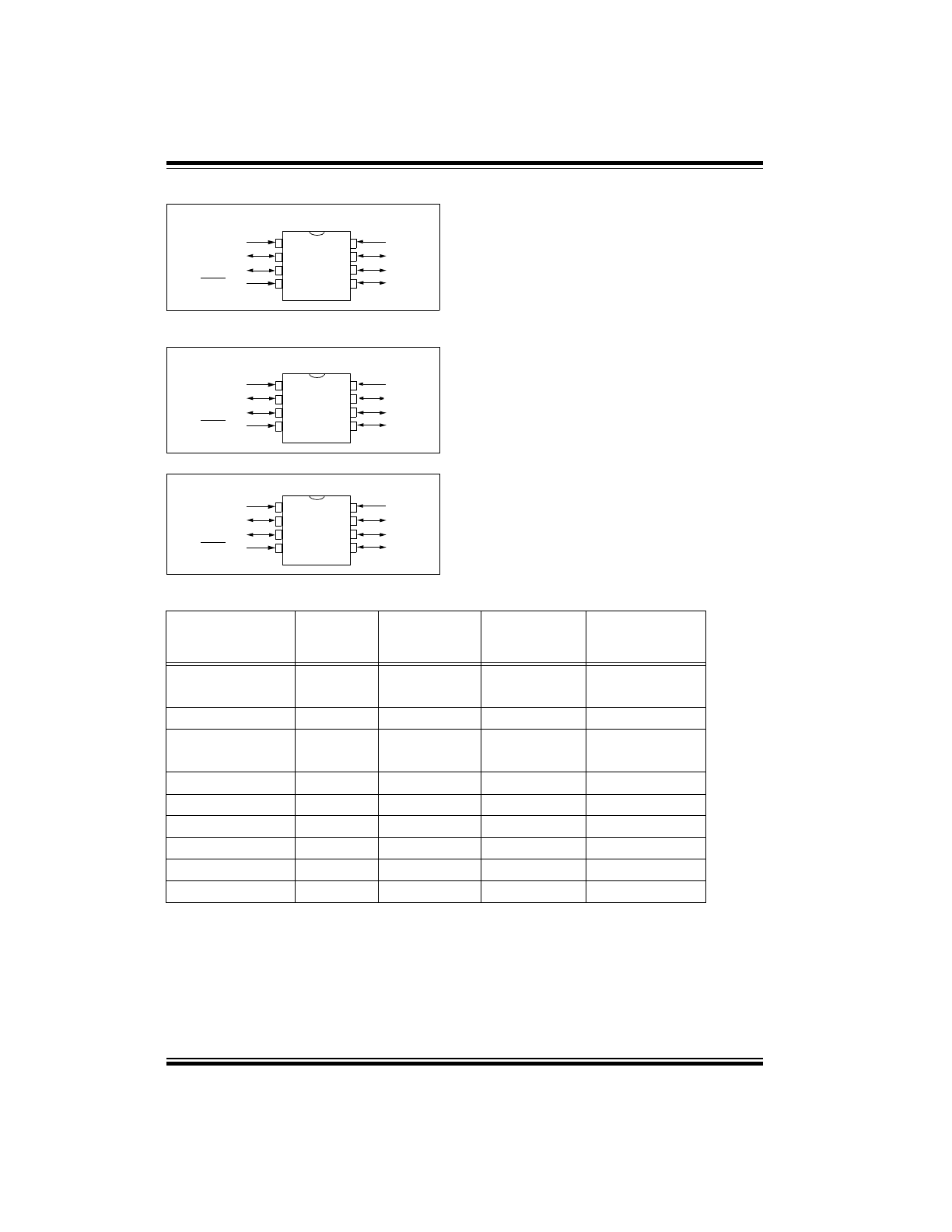
Pin Diagram - PIC12C508/509
Pin Diagram - PIC12C508A/509A,
PIC12CE518/519
Pin Diagram - PIC12CR509A
PDIP, 208 mil SOIC, Windowed Ceramic Side Brazed
8
7
6
5
1
2
3
4
V
SS
GP0
GP1
GP2/T0CKI
GP5/OSC1/CLKIN
GP4/OSC2
GP3/MCLR/V
PP
V
DD
PI
C1
2C
508
PI
C1
2C
509
PDIP, 150 & 208 mil SOIC, Windowed CERDIP
8
7
6
5
1
2
3
4
PI
C
1
2C
E51
8
V
SS
GP0
GP1
GP2/T0CKI
PI
C
1
2C
E51
9
GP5/OSC1/CLKIN
GP4/OSC2
GP3/MCLR/V
PP
V
DD
PI
C1
2C
508
A
PI
C
12C
509A
PDIP, 150 & 208 mil SOIC
8
7
6
5
1
2
3
4
V
SS
GP0
GP1
GP2/T0CKI
PI
C1
2C
R5
09
A
GP5/OSC1/CLKIN
GP4/OSC2
GP3/MCLR/V
PP
V
DD
Device Differences
Note 1: If you change from the PIC12C50X to the PIC12C50XA or to the PIC12CR50XA, please verify
oscillator characteristics in your application.
Note 2: See Section 7.2.5 for OSCCAL implementation differences.
Device
Voltage
Range
Oscillator
Oscillator
Calibration
2
(Bits)
Process
Technology
(Microns)
PIC12C508A
3.0-5.5
See Note 1
6
0.7
PIC12LC508A
2.5-5.5
See Note 1
6
0.7
PIC12C508
2.5-5.5
See Note 1
4
0.9
PIC12C509A
3.0-5.5
See Note 1
6
0.7
PIC12LC509A
2.5-5.5
See Note 1
6
0.7
PIC12C509
2.5-5.5
See Note 1
4
0.9
PIC12CR509A
2.5-5.5
See Note 1
6
0.7
PIC12CE518
3.0-5.5
-
6
0.7
PIC12LCE518
2.5-5.5
-
6
0.7
PIC12CE519
3.0-5.5
-
6
0.7
PIC12LCE519
2.5-5.5
-
6
0.7

1999 Microchip Technology Inc.
DS40139E-page 3
PIC12C5XX
TABLE OF CONTENTS
1.0
General Description............................................................................................................................................... 4
2.0
PIC12C5XX Device Varieties ................................................................................................................................ 7
3.0
Architectural Overview........................................................................................................................................... 9
4.0
Memory Organization .......................................................................................................................................... 13
5.0
I/O Port ................................................................................................................................................................ 21
6.0
Timer0 Module and TMR0 Register .................................................................................................................... 25
7.0
EEPROM Peripheral Operation ........................................................................................................................... 29
8.0
Special Features of the CPU ............................................................................................................................... 35
9.0
Instruction Set Summary ..................................................................................................................................... 47
10.0 Development Support.......................................................................................................................................... 59
11.0 Electrical Characteristics - PIC12C508/PIC12C509 ............................................................................................ 65
12.0 DC and AC Characteristics - PIC12C508/PIC12C509 ........................................................................................ 75
13.0 Electrical Characteristics PIC12C508A/PIC12C509A/PIC12LC508A/PIC12LC509A/PIC12CR509A/
PIC12CE518/PIC12CE519/
PIC12LCE518/PIC12LCE519/PIC12LCR509A ................................................................................................... 79
14.0 DC and AC Characteristics
PIC12C508A/PIC12C509A/PIC12LC508A/PIC12LC509A/PIC12CE518/PIC12CE519/PIC12CR509A/
PIC12LCE518/PIC12LCE519/ PIC12LCR509A .................................................................................................. 93
15.0 Packaging Information......................................................................................................................................... 99
Index ........................................................................................................................................................................... 105
PIC12C5XX Product Identification System ................................................................................................................ 109
Sales and Support: ..................................................................................................................................................... 109
To Our Valued Customers
Most Current Data Sheet
To obtain the most up-to-date version of this data sheet, please register at our Worldwide Web site at:
http://www.microchip.com
You can determine the version of a data sheet by examining its literature number found on the bottom outside corner
of any page. The last character of the literature number is the version number. e.g., DS30000A is version A of doc-
ument DS30000.
Errata
An errata sheet may exist for current devices, describing minor operational differences (from the data sheet) and rec-
ommended workarounds. As device/documentation issues become known to us, we will publish an errata sheet. The
errata will specify the revision of silicon and revision of document to which it applies.
To determine if an errata sheet exists for a particular device, please check with one of the following:
• Microchip’s Worldwide Web site; http://www.microchip.com
• Your local Microchip sales office (see last page)
• The Microchip Corporate Literature Center; U.S. FAX: (602) 786-7277
When contacting a sales office or the literature center, please specify which device, revision of silicon and data sheet
(include literature number) you are using.
Corrections to this Data Sheet
We constantly strive to improve the quality of all our products and documentation. We have spent a great deal of time
to ensure that this document is correct. However, we realize that we may have missed a few things. If you find any
information that is missing or appears in error, please:
• Fill out and mail in the reader response form in the back of this data sheet.
• E-mail us at webmaster@microchip.com.
We appreciate your assistance in making this a better document.

PIC12C5XX
DS40139E-page 4
1999 Microchip Technology Inc.
1.0
GENERAL DESCRIPTION
The PIC12C5XX from Microchip Technology is a fam-
ily of low-cost, high performance, 8-bit, fully static,
EEPROM/EPROM/ROM-based CMOS microcontrol-
lers. It employs a RISC architecture with only 33 sin-
gle word/single cycle instructions. All instructions are
single cycle (1
µ
s) except for program branches
which take two cycles. The PIC12C5XX delivers per-
formance an order of magnitude higher than its com-
petitors in the same price category. The 12-bit wide
instructions are highly symmetrical resulting in 2:1
code compression over other 8-bit microcontrollers in
its class. The easy to use and easy to remember
instruction set reduces development time signifi-
cantly.
The PIC12C5XX products are equipped with special
features that reduce system cost and power require-
ments. The Power-On Reset (POR) and Device Reset
Timer (DRT) eliminate the need for external reset cir-
cuitry. There are four oscillator configurations to choose
from, including INTRC internal oscillator mode and the
power-saving LP (Low Power) oscillator mode. Power
saving SLEEP mode, Watchdog Timer and code
protection features also improve system cost, power
and reliability.
The PIC12C5XX are available in the cost-effective
One-Time-Programmable (OTP) versions which are
suitable for production in any volume. The customer
can take full advantage of Microchip’s price leadership
in OTP microcontrollers while benefiting from the OTP’s
flexibility.
The PIC12C5XX products are supported by a full-fea-
tured macro assembler, a software simulator, an in-cir-
cuit emulator, a ‘C’ compiler, fuzzy logic support tools,
a low-cost development programmer, and a full fea-
tured programmer. All the tools are supported on IBM
PC and compatible machines.
1.1
Applications
The PIC12C5XX series fits perfectly in applications
ranging from personal care appliances and security
systems to low-power remote transmitters/receivers.
The EPROM technology makes customizing applica-
tion programs (transmitter codes, appliance settings,
receiver frequencies, etc.) extremely fast and conve-
nient, while the EEPROM data memory technology
allows for the changing of calibration factors and secu-
rity codes. The small footprint packages, for through
hole or surface mounting, make this microcontroller
series perfect for applications with space limitations.
Low-cost, low-power, high performance, ease of use
and I/O flexibility make the PIC12C5XX series very ver-
satile even in areas where no microcontroller use has
been considered before (e.g., timer functions, replace-
ment of “glue” logic and PLD’s in larger systems, copro-
cessor applications).
1999 Microchip Technology Inc.
DS40139E-page 5
PIC12C5XX
TABLE 1-1:
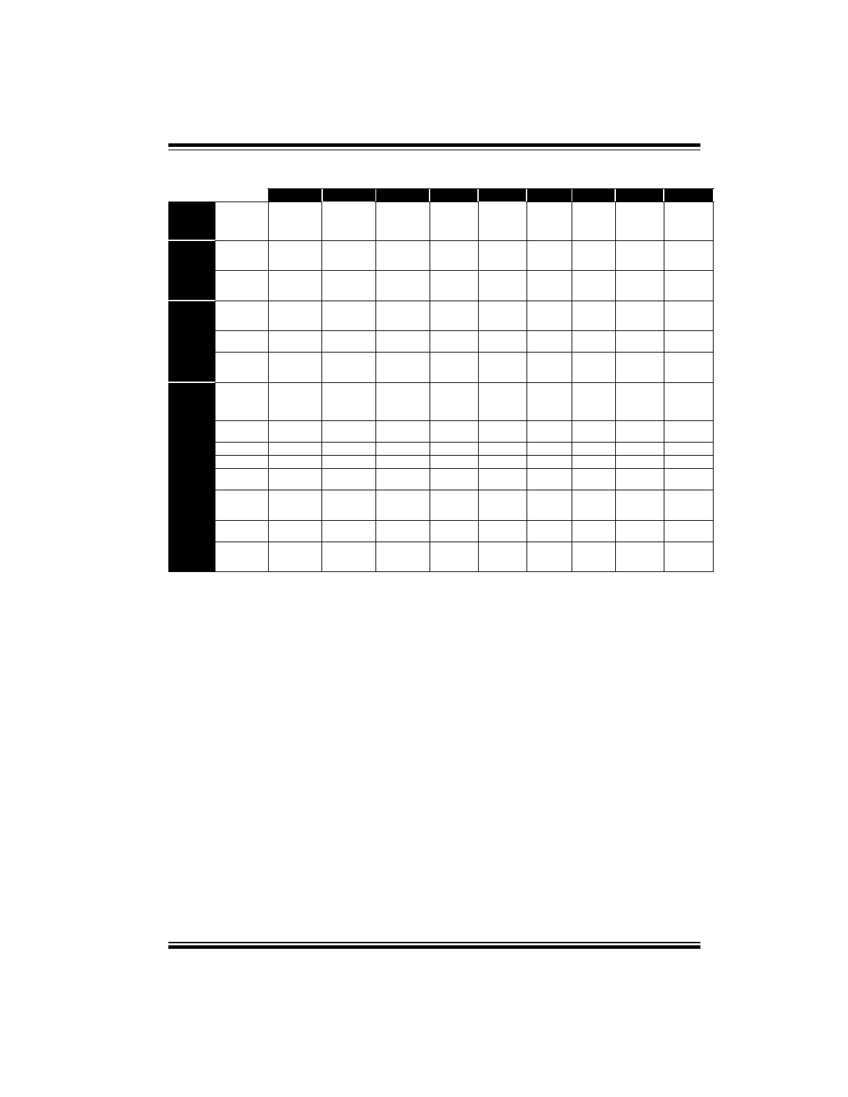
PIC12CXXX & PIC12CEXXX FAMILY OF DEVICES
PIC12C508(A) PIC12C509(A) PIC12CR509A PIC12CE518 PIC12CE519 PIC12C671 PIC12C672 PIC12CE673 PIC12CE674
Clock
Maximum
Frequency
of Operation
(MHz)
4
4
4
4
4
10
10
10
10
Memory
EPROM
Program
Memory
512 x 12
1024 x 12
1024 x 12
(ROM)
512 x 12
1024 x 12
1024 x 14
2048 x 14
1024 x 14
2048 x 14
RAM Data
Memory
(bytes)
25
41
41
25
41
128
128
128
128
Peripherals
EEPROM
Data Memory
(bytes)
—
—
—
16
16
—
—
16
16
Timer
Module(s)
TMR0
TMR0
TMR0
TMR0
TMR0
TMR0
TMR0
TMR0
TMR0
A/D Con-
verter (8-bit)
Channels
—
—
—
—
—
4
4
4
4
Features
Wake-up
from SLEEP
on pin
change
Yes
Yes
Yes
Yes
Yes
Yes
Yes
Yes
Yes
Interrupt
Sources
—
—
—
4
4
4
4
I/O Pins
5
5
5
5
5
5
5
5
5
Input Pins
1
1
1
1
1
1
1
1
1
Internal
Pull-ups
Yes
Yes
Yes
Yes
Yes
Yes
Yes
Yes
Yes
In-Circuit
Serial
Programming
Yes
Yes
—
Yes
Yes
Yes
Yes
Yes
Yes
Number of
Instructions
33
33
33
33
33
35
35
35
35
Packages
8-pin DIP,
JW, SOIC
8-pin DIP,
JW, SOIC
8-pin DIP,
SOIC
8-pin DIP,
JW, SOIC
8-pin DIP,
JW, SOIC
8-pin DIP,
JW, SOIC
8-pin DIP,
JW, SOIC
8-pin DIP,
JW
8-pin DIP,
JW
All PIC12CXXX & PIC12CEXXX devices have Power-on Reset, selectable Watchdog Timer, selectable code protect and high I/O
current capability.
All PIC12CXXX & PIC12CEXXX devices use serial programming with data pin GP0 and clock pin GP1.

PIC12C5XX
DS40139E-page 6
1999 Microchip Technology Inc.
NOTES:

1999 Microchip Technology Inc.
DS40139E-page 7
PIC12C5XX
2.0
PIC12C5XX DEVICE VARIETIES
A variety of packaging options are available.
Depending on application and production
requirements, the proper device option can be
selected using the information in this section. When
placing orders, please use the PIC12C5XX Product
Identification System at the back of this data sheet to
specify the correct part number.
2.1
UV Erasable Devices
The UV erasable version, offered in ceramic side
brazed package, is optimal for prototype development
and pilot programs.
The UV erasable version can be erased and
reprogrammed to any of the configuration modes.
Microchip’s PICSTART
PLUS and PRO MATE
pro-
grammers all support programming of the PIC12C5XX.
Third party programmers also are available; refer to the
Microchip Third Party Guide for a list of sources.
2.2
One-Time-Programmable (OTP)
Devices
The availability of OTP devices is especially useful for
customers who need the flexibility for frequent code
updates or small volume applications.
The OTP devices, packaged in plastic packages permit
the user to program them once. In addition to the
program memory, the configuration bits must also be
programmed.
Note:
Please note that erasing the device will
also erase the pre-programmed internal
calibration value for the internal oscillator.
The calibration value must be saved prior
to erasing the part.
2.3
Quick-Turnaround-Production (QTP)
Devices
Microchip offers a QTP Programming Service for
factory production orders. This service is made
available for users who choose not to program a
medium to high quantity of units and whose code
patterns have stabilized. The devices are identical to
the OTP devices but with all EPROM locations and fuse
options already programmed by the factory. Certain
code and prototype verification procedures do apply
before production shipments are available. Please con-
tact your local Microchip Technology sales office for
more details.
2.4
Serialized Quick-Turnaround
Production (SQTP
SM
) Devices
Microchip offers a unique programming service where
a few user-defined locations in each device are
programmed with different serial numbers. The serial
numbers may be random, pseudo-random or
sequential.
Serial programming allows each device to have a
unique number which can serve as an entry-code,
password or ID number.
2.5
Read Only Memory (ROM) Device
Microchip offers masked ROM to give the customer a
low cost option for high volume, mature products.

PIC12C5XX
DS40139E-page 8
1999 Microchip Technology Inc.
NOTES:
1999 Microchip Technology Inc.
DS40139E-page 9
PIC12C5XX
3.0
ARCHITECTURAL OVERVIEW
The high performance of the PIC12C5XX family can
be attributed to a number of architectural features
commonly found in RISC microprocessors. To begin
with, the PIC12C5XX uses a Harvard architecture in
which program and data are accessed on separate
buses. This improves bandwidth over traditional von
Neumann architecture where program and data are
fetched on the same bus. Separating program and
data memory further allows instructions to be sized
differently than the 8-bit wide data word. Instruction
opcodes are 12-bits wide making it possible to have all
single word instructions. A 12-bit wide program
memory access bus fetches a 12-bit instruction in a
single cycle. A two-stage pipeline overlaps fetch and
execution of instructions. Consequently, all instructions
(33) execute in a single cycle (1
µ
s @ 4MHz) except for
program branches.
The table below lists program memory (EPROM), data
memory (RAM), ROM memory, and non-volatile
(EEPROM) for each device.
The PIC12C5XX can directly or indirectly address its
register files and data memory. All special function
registers including the program counter are mapped in
the data memory. The PIC12C5XX has a highly
orthogonal (symmetrical) instruction set that makes it
possible to carry out any operation on any register
using any addressing mode. This symmetrical nature
and lack of ‘special optimal situations’ make
programming with the PIC12C5XX simple yet efficient.
In addition, the learning curve is reduced significantly.
Device
Memory
EPROM
Program
ROM
Program
RAM
Data
EEPROM
Data
PIC12C508
512 x 12
25
PIC12C509
1024 x 12
41
PIC12C508A
512 x 12
25
PIC12C509A
1024 x 12
41
PIC12CR509A
1024 x 12
41
PIC12CE518
512 x 12
25 x 8
16 x 8
PIC12CE519
1024 x 12
41 x 8
16 x 8
The PIC12C5XX device contains an 8-bit ALU and
working register. The ALU is a general purpose
arithmetic unit. It performs arithmetic and Boolean
functions between data in the working register and any
register file.
The ALU is 8-bits wide and capable of addition,
subtraction, shift and logical operations. Unless
otherwise mentioned, arithmetic operations are two's
complement in nature. In two-operand instructions,
typically one operand is the W (working) register. The
other operand is either a file register or an immediate
constant. In single operand instructions, the operand is
either the W register or a file register.
The W register is an 8-bit working register used for
ALU operations. It is not an addressable register.
Depending on the instruction executed, the ALU may
affect the values of the Carry (C), Digit Carry (DC),
and Zero (Z) bits in the STATUS register. The C and
DC bits operate as a borrow and digit borrow out bit,
respectively, in subtraction. See the
SUBWF
and
ADDWF
instructions for examples.
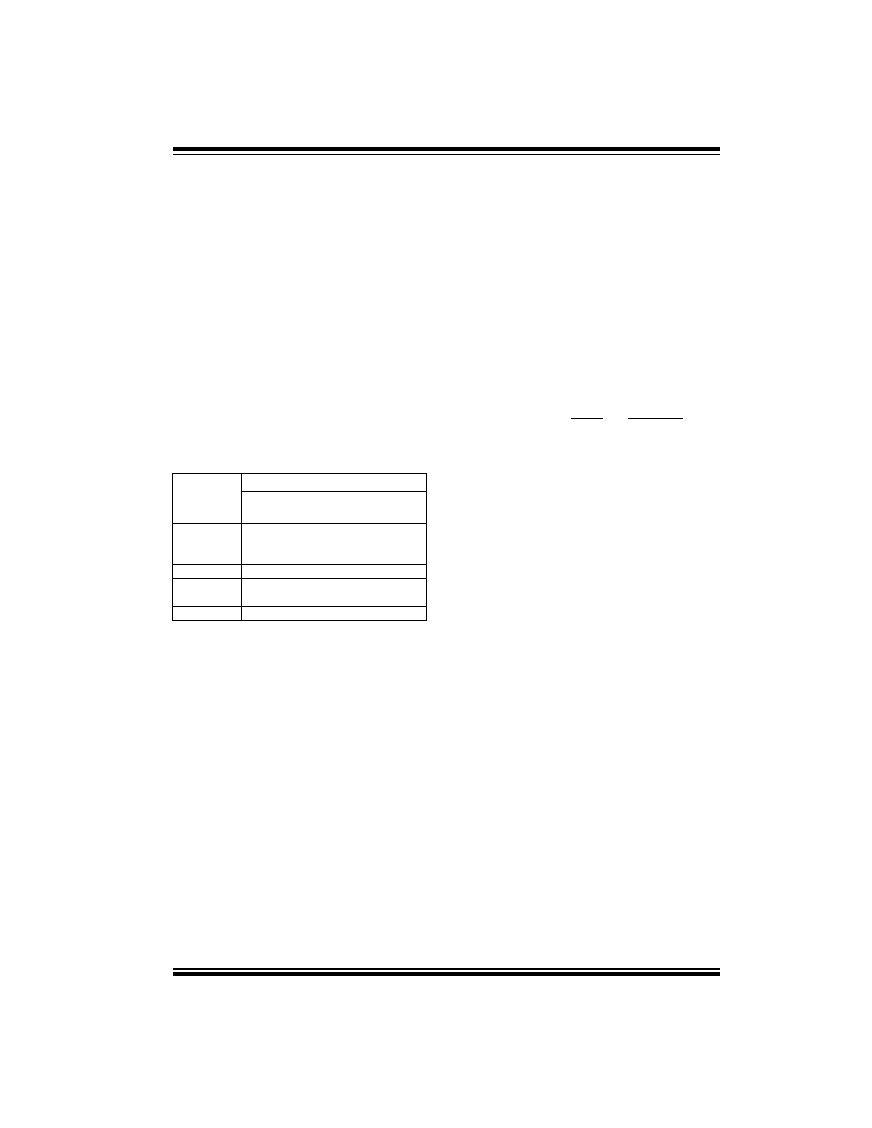
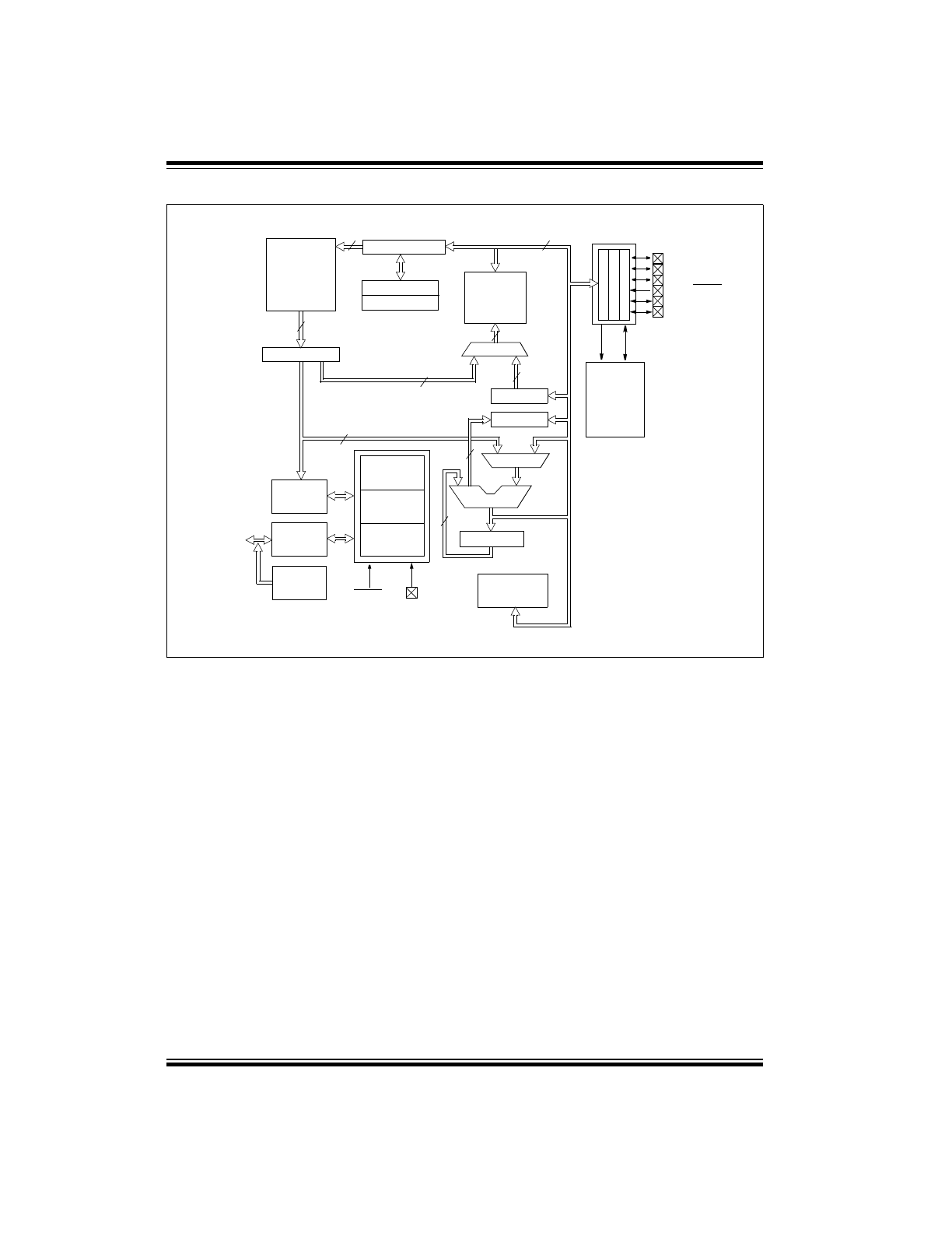
A simplified block diagram is shown in Figure 3-1, with
the corresponding device pins described in Table 3-1.
PIC12C5XX
DS40139E-page 10
1999 Microchip Technology Inc.
FIGURE 3-1:
PIC12C5XX BLOCK DIAGRAM
Device Reset
Timer
Power-on
Reset
Watchdog
Timer
ROM/EPROM
Program
Memory
12
Data Bus
8
12
Program
Bus
Instruction reg
Program Counter
RAM
File
Registers
Direct Addr
5
RAM Addr
9
Addr MUX
Indirect
Addr
FSR reg
STATUS reg
MUX
ALU
W reg
Instruction
Decode &
Control
Timing
Generation
OSC1/CLKIN
OSC2
MCLR
V
DD
, V
SS
Timer0
GPIO
8
8
GP4/OSC2
GP3/MCLR/V
PP
GP2/T0CKI
GP1
GP0
5-7
3
GP5/OSC1/CLKIN
STACK1
STACK2
512 x 12 or
25 x 8 or
1024 x 12
41 x 8
Internal RC
OSC
16 X 8
EEPROM
Data
Memory
PIC12CE5XX
Only
SD
A
SC
L