
© 2007 Microchip Technology Inc.
DS21372D-page 1
TC125/TC126
Features:
• Assured Start-up at 0.9V
• PFM (100 kHz Max. Operating Frequency)
• 40
μA Maximum Supply Current
(V
OUT
= 3V @ 30 mA)
• 0.5
μA Shutdown Mode (TC125)
• Voltage Sense Input (TC126)
• Requires Only Three External Components
• 80 mA Maximum Output Current
• Small Package: 5-Pin SOT-23
Applications:
• Palmtops/PDAs
• Battery-Operated Systems
• Cameras
• Portable Communicators
Device Selection Table
*Other output voltages are available. Please contact
Microchip Technology Inc. for details.
Package Type
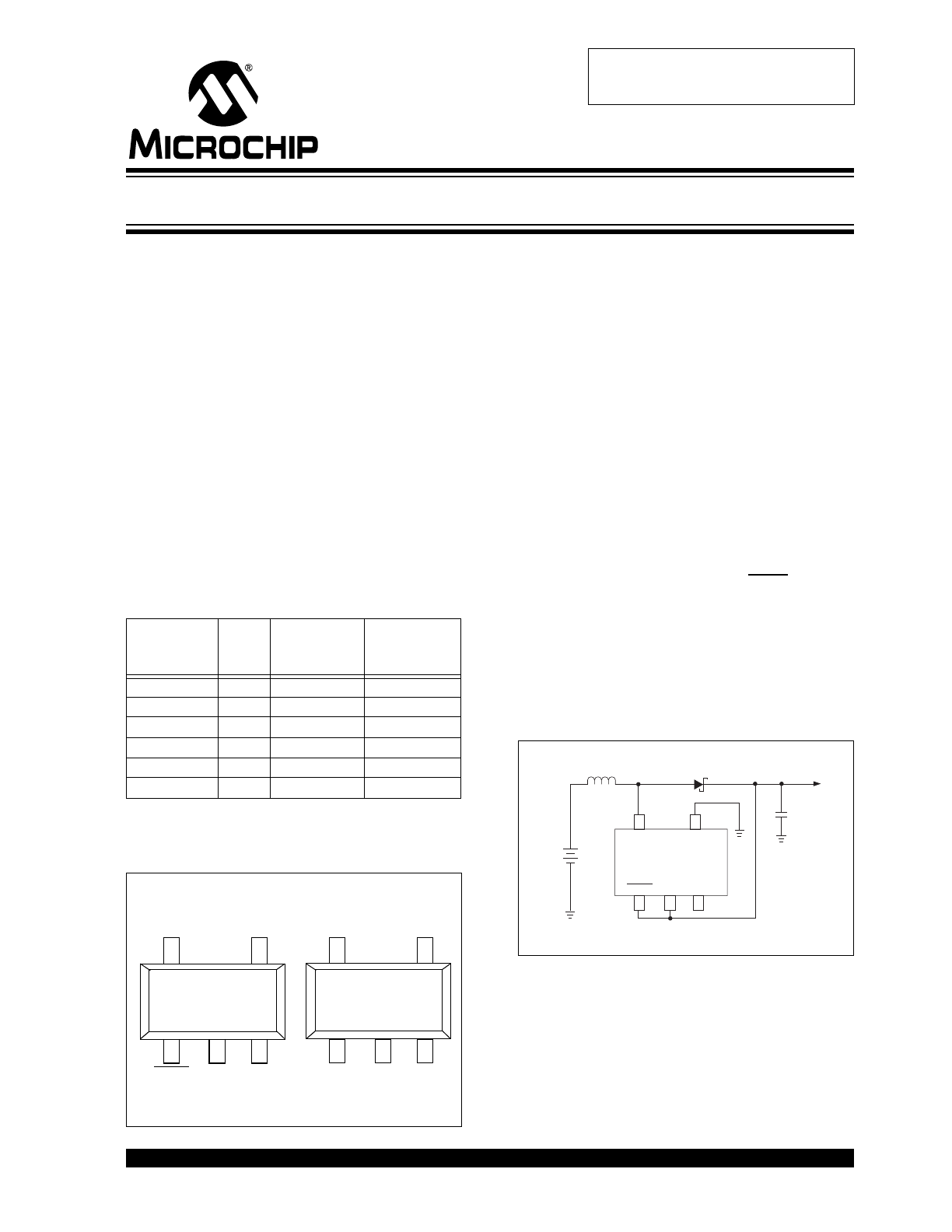
General Description:
The TC125/126 step-up (Boost) switching regulators
furnish output currents to a maximum of 80 mA
(V
IN
= 2V, V
OUT
= 3V) with typical efficiencies above
80%. These devices employ pulse frequency modula-
tion (PFM) for minimum supply current at low loads.
They are ideal for battery-operated applications
powered from one or more cells. Maximum supply
current is less than 70
μA at full output load, and less
than 5
μA in standby (V
OUT
= 3V). Both devices require
only an external inductor, diode, and capacitor to
implement a complete DC/DC regulator.
The TC126 has separate output voltage sensing and
chip power inputs for greater application flexibility. The
TC125 combines the output voltage sensing and chip
power inputs onto a single package pin, but adds a
power-saving Shutdown mode that suspends regulator
operation and reduces supply current to less than 0.5
μA when the shutdown control input (SHDN) is low.
The TC125/TC126 are available in a small 5-Pin
SOT-23 package, occupy minimum board space and
use small external components. The TC125 accepts
input voltages from 2V to 10V. The TC126 accepts
input voltages from 2.2V to 10V. Both the TC125 and
TC126 have a start-up voltage of 0.9V at light load.
Typical Application
Part
Number
Output
Voltage
(V)*
Package
Operating
Temp.
Range
TC125501ECT
5.0
5-Pin SOT-23
-40
°C to +85°C
TC125331ECT
3.3
5-Pin SOT-23
-40
°C to +85°C
TC125301ECT
3.0
5-Pin SOT-23
-40
°C to +85°C
TC126501ECT
5.0
5-Pin SOT-23
-40
°C to +85°C
TC126331ECT
3.3
5-Pin SOT-23
-40
°C to +85°C
TC126301ECT
3.0
5-Pin SOT-23
-40
°C to +85°C
5-Pin SOT-23
NOTE: 5-Pin SOT-23 is equivalent to the EIAJ SC-74A
V
DD
SENSE
TC125
1
2
3
5
4
PS
LX
GND
NC
SHDN
TC126
1
2
3
5
4
LX
GND
NC
3V
2 x "AA"
Cell
+
–
Two Cell to 5V Boost Regulator
1
2
3
5
4
TC125
LX
SHDN
NC
PS
GND
MA735
+
V
IN
Sumida
100 mH CD54
V
OUT
5V @80 mA
47
µ
F/16V
Tantalum
PFM Step-Up DC/DC Regulators
Obsolete Device
TC125/TC126
DS21372D-page 2
© 2007 Microchip Technology Inc.
1.0
ELECTRICAL
CHARACTERISTICS
Absolute Maximum Ratings*
Voltage on V
DD
, SENSE/V
DD
, LX, SHDN Pins
....................................................... -0.3V to +12V
LX Sink Current ........................................... 400 mA pk
Power Dissipation............................................150 mW
Operating Temperature Range.............-40°C to +85°C
Storage Temperature Range ..............-40°C to +125°C
*Stresses above those listed under “Absolute
Maximum Ratings” may cause permanent damage to
the device. These are stress ratings only and functional
operation of the device at these or any other conditions
above those indicated in the operation sections of the
specifications is not implied. Exposure to Absolute
Maximum Rating conditions for extended periods may
affect device reliability.
TC125/TC126 ELECTRICAL SPECIFICATIONS
Electrical Characteristics: V
IN
= V
OUT
x 0.6, T
A
= 25°C, SHDN = V
OUT
(TC125), unless otherwise noted.
Symbol
Parameter
Min
Typ
Max
Units
Test Conditions
V
OUT
Output Voltage
V
R
– 2.5%
V
R
± 0.5%
V
R
+ 2.5%
V
V
DD
Operating Supply Voltage
0.70
—
10.0
V
Note 4
V
START
Start-Up Supply Voltage
—
0.80
0.90
V
I
OUT
= 1
m
A
I
DD
Operating Supply Current
TC125
TC125/126
TC125/126
—
—
—
14
20
32
28
40
64
μA (Note 2)
V
OUT
=
2V,
I
OUT
= 10 mA
V
OUT
=
3V,
I
OUT
= 30 mA
V
OUT
=
5V,
I
OUT
= 50 mA
I
NL
No Load Supply Current
—
—
—
5
5
6
9
10
11
μA I
OUT
= 0, V
OUT
=
2V
V
OUT
=
3V
V
OUT
=
5V
I
STBY
Standby Supply Current
—
—
—
2
3
3
4
5
5
μA
V
IN
= V
OUT
+ 0.5V,
V
IN
=
2V
V
IN
=
3V
V
IN
=
5V
Ishdn
Shutdown Supply Current
—
—
0.5
μA SHDN = V
IL
,
(Note 2)
R
LX(ON)
LX Pin ON Resistance
—
—
—
10
6
3
14
8
5
W
V
LX
= 0.4V, V
OUT
=
2V
V
OUT
=
3V
V
OUT
=
5V
(Note 2), (Note 3)
I
LX
LX Pin Leakage Current
—
—
1
μA No external components,
V
OUT
=
V
LX
= 10V
D
CYCLE
Duty Cycle
70
75
80
%
Measured at LX pin (Note 2)
f
MAX
Maximum Oscillator Frequency
85
100
115
kHz Note 2
VLX
LIM
LX Pin Limit Voltage
0.7
—
1.1
V
Note 2
h
Efficiency
—
—
—
70
80
85
—
—
—
%
V
OUT
=
2V
V
OUT
=
3V
V
OUT
=
5V
V
IH
SHDN Input Logic High
0.75
—
—
V
V
IL
SHDN Input Logic Low
—
—
0.20
V
II
Nh
SHDN Input Current (High)
—
—
0.25
μA
II
Nl
SHDN Pin Input Current (Low)
-0.25
—
—
μA
Note 1: V
R
is the factory output voltage setting.
2: V
IN
= V
OUT
x 0.95.
3: V
DD
input tied to SENSE input for TC126, as shown in Figure 3-2.
4: The V
PS
input of the TC125 must be operated between 2.0V and 10.0V for spec compliance.
The V
DD
input of the TC126 must be operated between 2.2V and 10.0V for spec compliance.
© 2007 Microchip Technology Inc.
DS21372D-page 3
TC125/TC126
2.0
PIN DESCRIPTIONS
The descriptions of the pins are listed in Table 2-1.
TABLE 2-1:
PIN FUNCTION TABLE
TC125
Pin No.
(5-Pin SOT-23)
TC126
Pin No.
(5-Pin SOT-23)
Symbol
Description
1
—
SHDN
Shutdown input. A logic low on this input suspends device opera-
tion and supply current is reduced to less than 0.5
μA. The device
resumes normal operation when SHDN is again brought high.
—
1
SENSE
Voltage sense input. This input provides feedback voltage sensing
to the internal error amplifier. It must be connected to the output
voltage node, preferably the single point in the system where tight
voltage regulation is most beneficial.
2
—
PS
Power and voltage sense input. This dual function input provides
both feedback voltage sensing and internal chip power. It should
be connected to the regulator output. (See Figure 3-1).
—
2
V
DD
Power supply voltage input.
3
3
NC
Not connected.
4
4
GND
Ground terminal.
5
5
LX
Inductor switch output. LX is the drain of an internal N-channel
switching transistor. This terminal drives the external inductor,
which ultimately provides current to the load.
TC125/TC126
DS21372D-page 4
© 2007 Microchip Technology Inc.
3.0
DETAILED DESCRIPTION
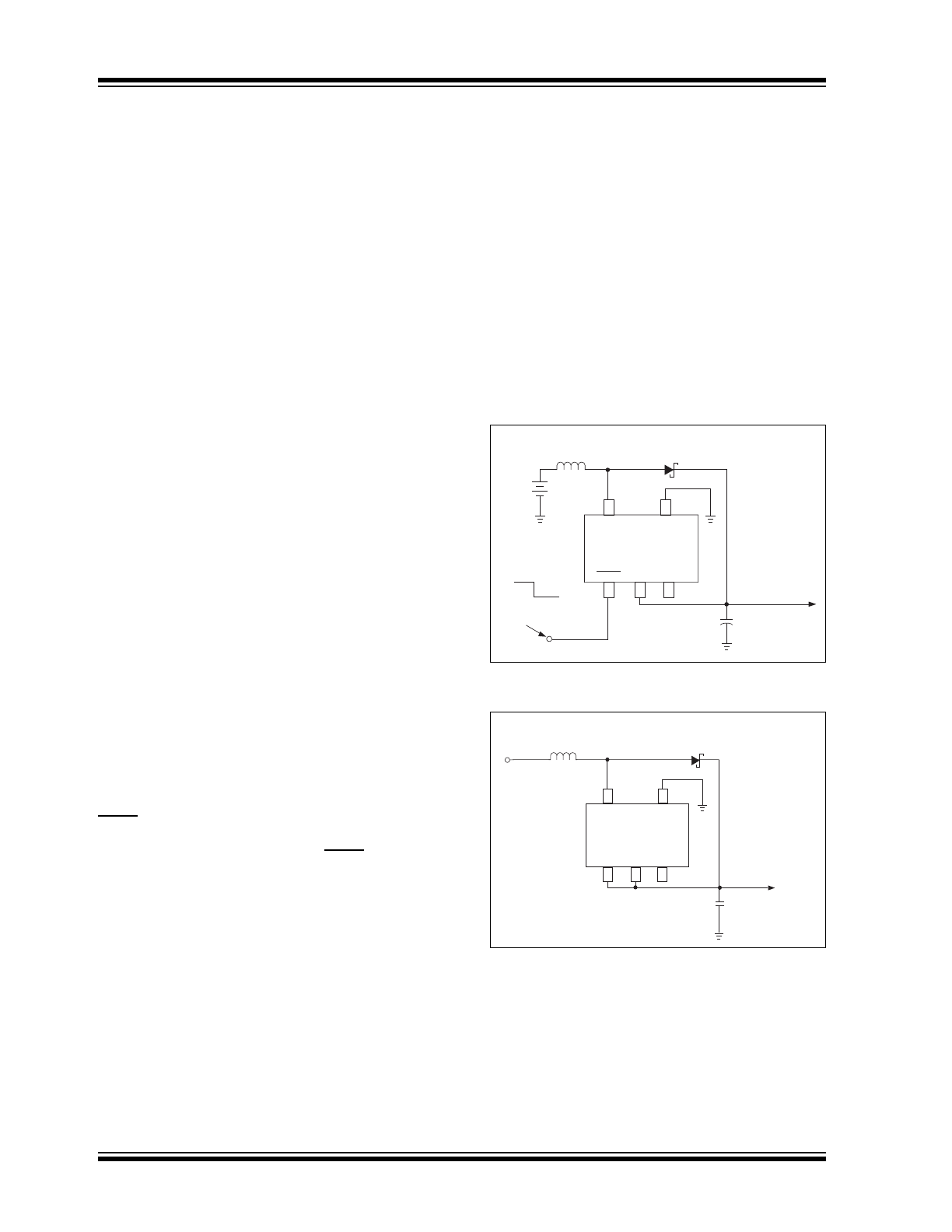
The TC125/126 are PFM step-up DC/DC regulators for
use in systems operating from two or more cells or in
low voltage, line powered applications. Because Pulse
Frequency Modulation (PFM) is used, the TC125/126
switching frequency (and therefore supply current) is
minimized at low output loads. This is especially
important in battery operated applications (such as
pagers) that operate in Standby mode most of the
time. For example, a TC125/126 with a 3V output and
no load will consume a maximum supply current of
only 10
μA versus a supply current of 40 μA maximum
when I
OUT
= 30 mA. Both devices require only an
external inductor, diode and capacitor to implement a
complete DC/DC converter.
The TC125 is recommended for applications requiring
Shutdown mode as a means of reducing system supply
current. The TC125 is powered from the PS input,
which must be connected to the regulated output as
shown in Figure 3-1. PS also senses output voltage for
closed-loop regulation. Start-up current is furnished
through the inductor when input voltage is initially
applied. This action starts the oscillator, causing the
voltage at the PS input to rise, bootstrapping the
regulator into full operation.
The TC126 (Figure 3-2) is recommended for all appli-
cations not requiring Shutdown mode. It has separate
V
DD
and SENSE inputs, allowing it to be powered from
any source of 2.2V to 10V in the system. The V
DD
input
of the TC126 may be connected to the V
IN
, V
OUT
, or an
external DC voltage. Lower values of V
DD
result in
lower supply current, but lower efficiency due to higher
switch ON resistance. Higher V
DD
values increase
supply current, but drive the internal switching
transistor harder (lowering RDS
ON
), thereby increasing
efficiency.
3.1
Low-Power Shutdown Mode
The TC125 enters a low-power Shutdown mode when
SHDN is brought low. While in shutdown, the oscillator
is disabled and the internal switch is shut off. Normal
regulator operation resumes when SHDN is brought
high. Because the TC125 uses an external diode, a
leakage path between the input voltage and the output
node (through the inductor and diode) exists while the
regulator is in shutdown. Care must be taken in system
design to assure the input supply is isolated from the
load during shutdown.
3.2
Behavior When V
IN
is Greater
Than the Factory-Programmed
OUT Setting
The TC125 and TC126 are designed to operate as
step-up regulators only. As such, V
IN
is assumed to
always be less than the factory-programmed output
voltage setting (V
R
). Operating the TC125/126 with
V
IN
> V
R
causes regulating action to be suspended
(and corresponding supply current reduction) until V
IN
is again less than V
R
. While regulating action is
suspended, V
IN
is connected to the output voltage node
through the series combination of the inductor and
Schottky diode. Again, care must be taken to add the
appropriate isolation (MOSFET series switch or post
LDO with shutdown) during system design if this V
IN
/
V
OUT
leakage path is problematic.
FIGURE 3-1:
Typical TC125 Circuit
FIGURE 3-2:
Typical TC126 Circuit
L1
100
µ
H Sumida CD54
D1
MA735
Shutdown
Control
1
2
3
5
4
TC125
LX
SHDN
NC
PS
GND
1.5V
ON
OFF
V
OUT
3.3V @40 mA
C
1
47
µ
F/16V
Tantalum
+
1
2
3
4
5
TC126
LX
SENSE
NC
V
DD
GND
3.3V
Line
Supply
L1
100
µ
H Sumida CD54
D1
MA735
V
OUT
5V @80 mA
C
1
47
µ
F/16V
Tantalum
+
© 2007 Microchip Technology Inc.
DS21372D-page 5
TC125/TC126
4.0
APPLICATIONS
4.1
Input Bypass Capacitors
Adding an input bypass capacitor reduces peak current
transients drawn from the input supply and reduces the
switching noise generated by the regulator. The source
impedance of the input supply determines the size of
the capacitor that should be used.
4.2
Inductor Selection
Selecting the proper inductor value is a trade-off
between physical size and power conversion require-
ments. Lower value inductors cost less, but result in
higher ripple current and core losses. They are also
more prone to saturate since the coil current ramps to
a higher value. Larger inductor values reduce both
ripple current and core losses, but are larger in physical
size and tend to increase the start-up time slightly. The
recommended inductor value for use with the TC125/
126 is 100
μH. Inductors with a ferrite core (or equiva-
lent) are recommended. For highest efficiency, use an
inductor with a series resistance less than 20 m
Ω.
4.3
Internal Transistor Switch Current
Limiting
The peak switch current is equal to the input voltage
divided by the RDS
ON
of the internal switch. The
internal transistor has absolute maximum current rating
of 400 mA with a design limit of 350 mA. A built-in
oscillator frequency doubling circuit guards against
high switching currents. Should the voltage on the LX
pin rise above 1.1V, max while the internal N-channel
switch is ON, the oscillator frequency automatically
doubles to minimize ON time. Although reduced, switch
current still flows because the regulator remains in
operation. Therefore, the LX input is not internally
current limited and care must be taken never to exceed
the 350 mA maximum limit. Failure to observe this will
result in damage to the regulator.
4.4
Output Diode
For best results, use a Schottky diode such as the
MA735, 1N5817, MBR0520L or equivalent. Connect
the diode between the PS and LX pins (TC125) or
SENSE and LX pins (TC126) as close to the IC as
possible. (Do not use ordinary rectifier diodes since the
higher threshold voltages reduce efficiency.)
4.5
Output Capacitor
The effective series resistance of the output capacitor
directly affects the amplitude of the output voltage
ripple. (The product of the peak inductor current and
the ESR determines output ripple amplitude.) There-
fore, a capacitor with the lowest possible ESR should
be selected. Smaller capacitors are acceptable for light
loads or in applications where ripple is not a concern.
The Sprague 595D series of tantalum capacitors are
among the smallest of all low ESR surface mount
capacitors available. Table 4-1 lists suggested
components and suppliers.
4.6
Board Layout Guidelines
As with all inductive switching regulators, the TC125/
126 generate fast switching waveforms that radiate
noise. Interconnecting lead lengths should be
minimized to keep stray capacitance, trace resistance,
and radiated noise as low as possible. In addition, the
GND pin, input bypass capacitor, and output filter
capacitor ground leads should be connected to a single
point. The input capacitor should be placed as close to
power and ground pins of the TC125/126 as possible.
TABLE 4-1:
SUGGESTED COMPONENTS AND SUPPLIERS
Type
Inductors
Capacitors
Diodes
Surface Mount
Sumida
CD54 Series
CDR125 Series
Coiltronics
CTX Series
Murata
LQN6C Series
Matsuo
267 Series
Murata
GRM200 Series
Sprague
595D Series
Nichicon
F93 Series
Nihon
EC10 Series
Matsushita
MA735 Series
Through-Hole
Sumida
RCH855 Series
RCH110 Series
Renco
RL1284-12
Sanyo
OS-CON Series
Nichicon
PL Series
ON Semiconductor
1N5817-1N5822
TC125/TC126
DS21372D-page 6
© 2007 Microchip Technology Inc.
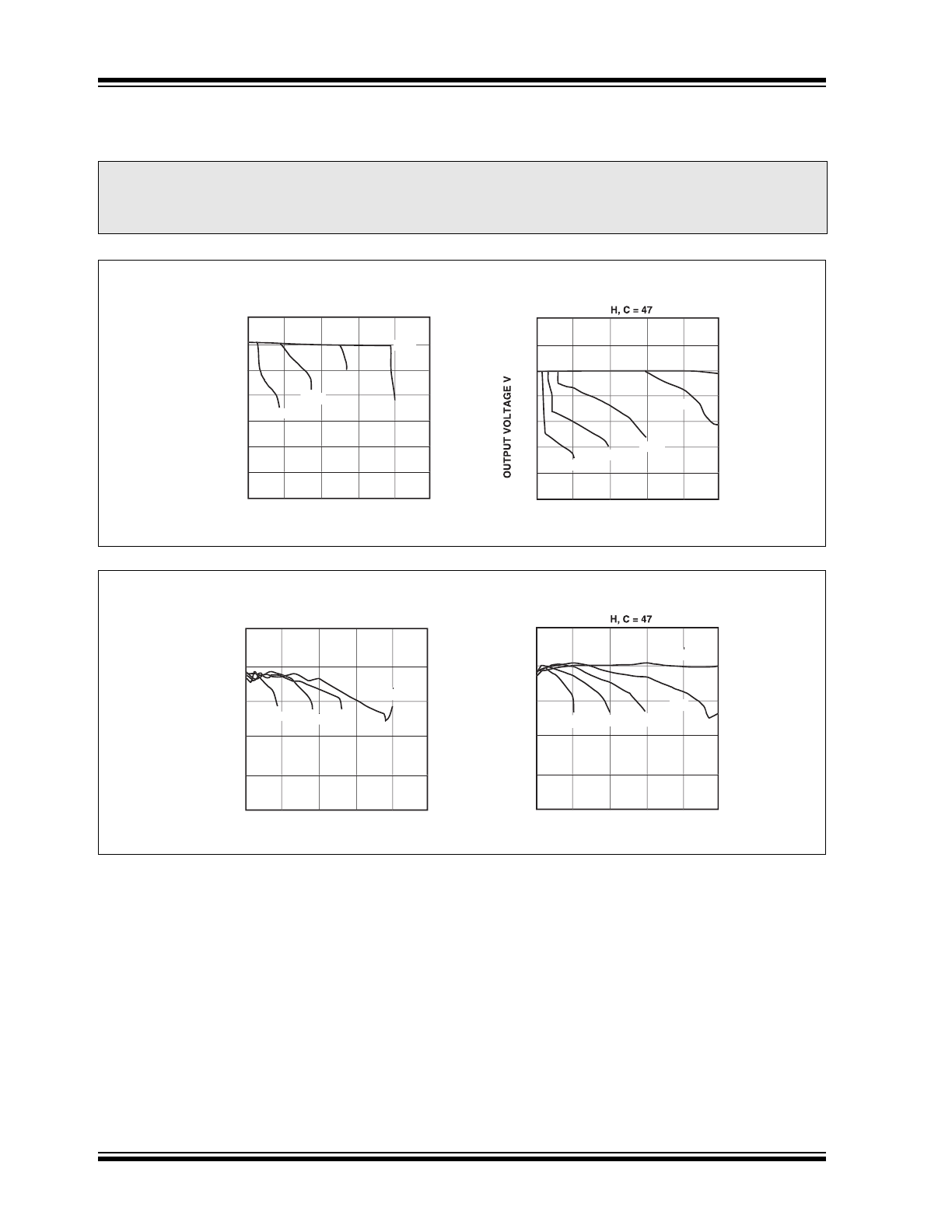
5.0
TYPICAL CHARACTERISTICS
(Unless Otherwise Specified, All Parts Are Measured At Temperature = 25°C)
Note:
The graphs and tables provided following this note are a statistical summary based on a limited number of
samples and are provided for informational purposes only. The performance characteristics listed herein
are not tested or guaranteed. In some graphs or tables, the data presented may be outside the specified
operating range (e.g., outside specified power supply range) and therefore outside the warranted range.
0
20
40
60
80
100
OUTPUT CURRENT I
OUT
(mA)
3.5
OUTPUT VOLTAGE V
OUT
(V)
Output Voltage vs. Output Current
TC125/126
0
1.0
2.0
2.5
L = 100
μ
H, C = 47
μ
F (Tantalum)
3.0
1.5
0.5
0
20
40
60
80
100
OUTPUT CURRENT I
OUT
(mA)
OUT
(V)
0
2
4
5
L = 100
μ
μ
F (Tantalum)
6
3
1
V
V
IN
IN
9V
= 0.9V
1.2V
V
1.2V
1.5V
1.8V
3.0V
3.0V
2.0V
1.5V
1.2V
V
V
IN
9V
= 0.9V
Output Voltage vs. Output Current
TC125/126
0
20
40
60
80
100
OUTPUT CURRENT I
OUT
(mA)
E
FFICIENCY EFFI
(%
)
Efficiency vs. Output Current
TC125/126
0
20
60
80
L = 100
µ
H, C = 47
µ
F (Tantalum)
100
40
0
20
40
60
80
100
OUTPUT CURRENT I
OUT
(mA)
E
FFICIENCY EFFI
(%
)
0
20
60
80
L = 100
µ
µ
F (Tantalum)
100
40
V
IN
= 1.8V
= 1.8V
1.5V
1.2V
V
1.2V
0.9V
V
V
IN
= 3.0V
= 3.0V
1.5V
1.2V
0.9V
2.0V
2.0V
Efficiency vs. Output Current
TC125/126
© 2007 Microchip Technology Inc.
DS21372D-page 7
TC125/TC126
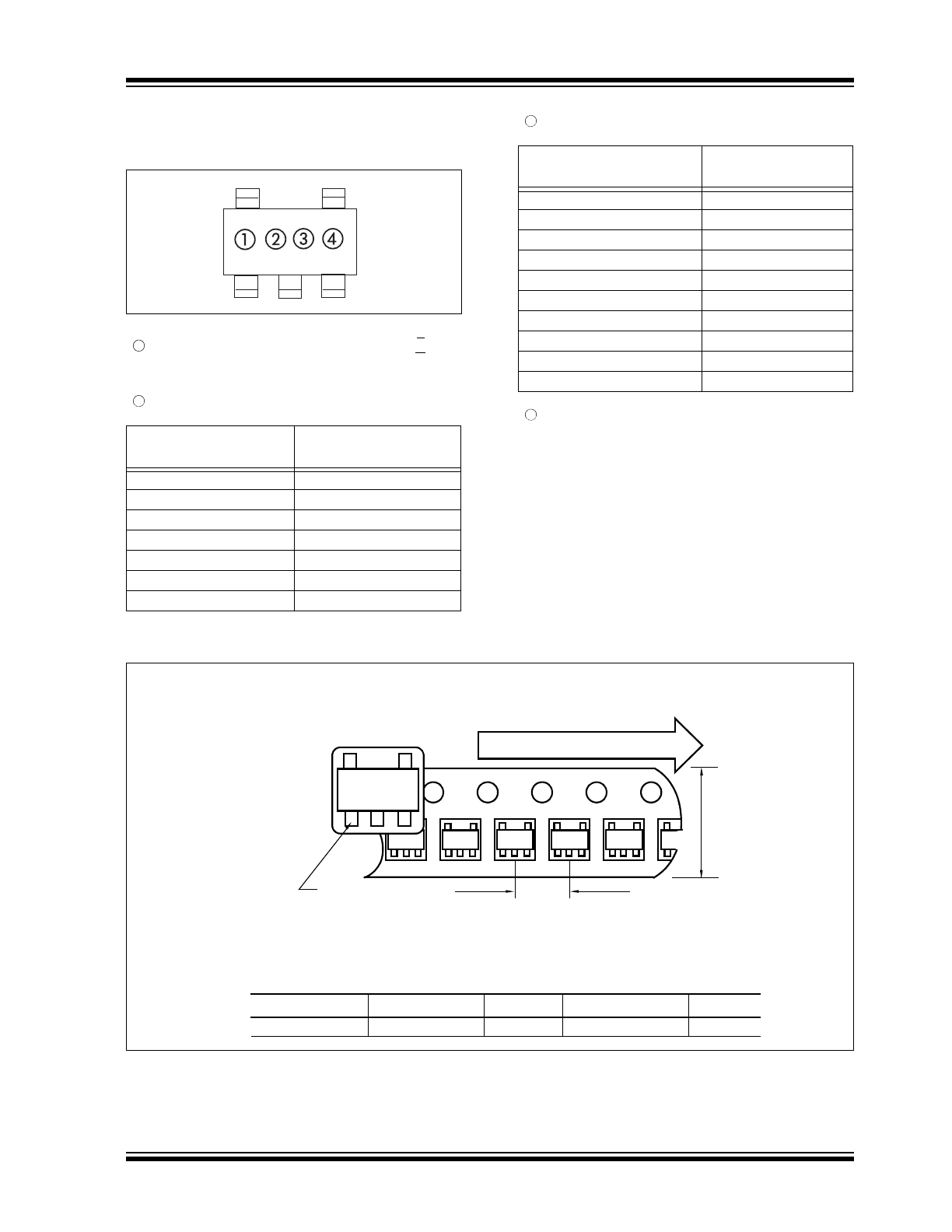
6.0
PACKAGING INFORMATION
6.1
Package Marking Information
6.2
Taping Form
Symbol
(100 kHz)
Voltage
1
1
2
2
3
3
4
4
5
5
6
6
7
7
1
represents product classification; TC125 = L
TC126 = N
2
represents first integer of voltage
Symbol
(100 kHz)
Voltage
0
.0
1
.1
2
.2
3
.3
4
.4
5
.5
6
.6
7
.7
8
.8
9
.9
3
represents first decimal of voltage
4
represents production lot ID code
Component Taping Orientation for 5-Pin SOT-23 (EIAJ SC-74A) Devices
Package
Carrier Width (W) Pitch (P)
Part Per Full Reel Reel Size
5-Pin SOT-23
8 mm
4 mm
3000
7 in
Carrier Tape, Number of Components Per Reel and Reel Size
User Direction of Feed
Device
Marking
Pin 1
Standard Reel Component Orientation
TR Suffix Device
(Mark Right Side Up)
W
P
TC125/TC126
DS21372D-page 8
© 2007 Microchip Technology Inc.
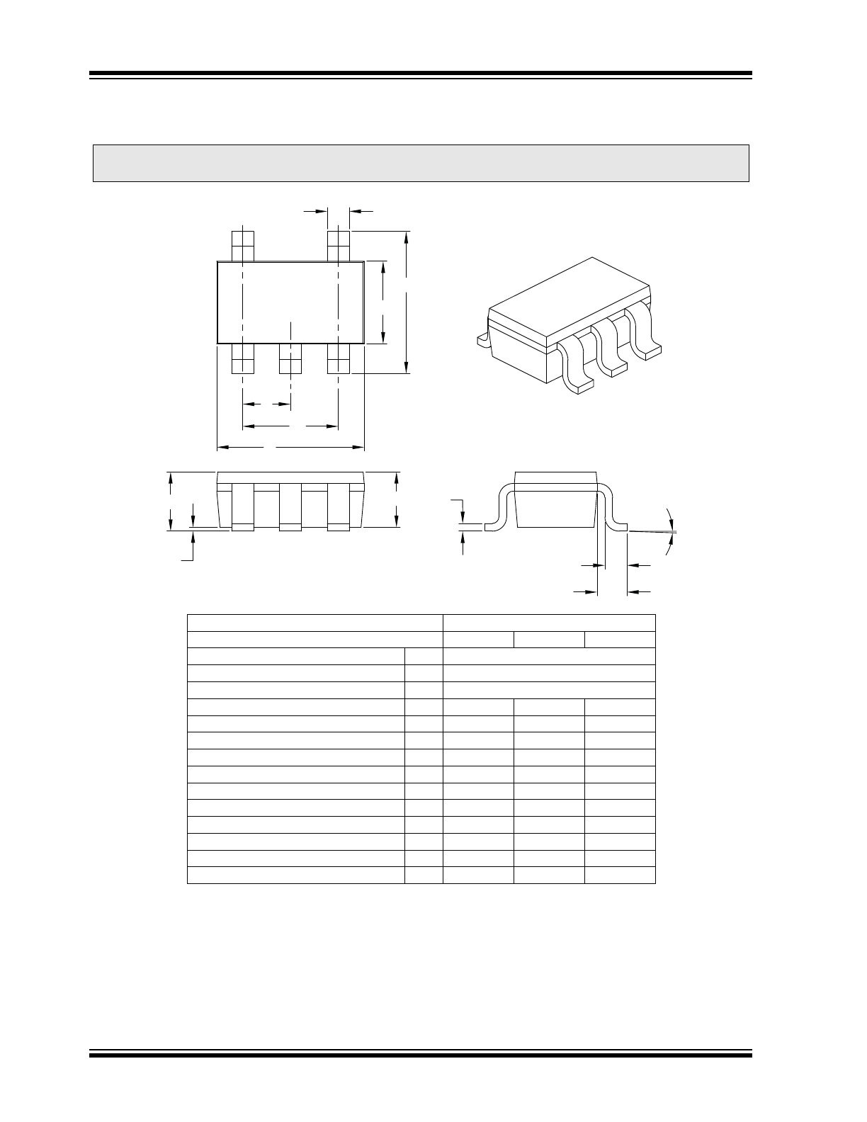
5-Lead Plastic Small Outline Transistor (OT or CT) [SOT-23]
Notes:
1. Dimensions D and E1 do not include mold flash or protrusions. Mold flash or protrusions shall not exceed 0.127 mm per side.
2. Dimensioning and tolerancing per ASME Y14.5M.
BSC: Basic Dimension. Theoretically exact value shown without tolerances.
Note:
For the most current package drawings, please see the Microchip Packaging Specification located at
http://www.microchip.com/packaging
Units
MILLIMETERS
Dimension Limits
MIN
NOM
MAX
Number of Pins
N
5
Lead Pitch
e
0.95 BSC
Outside Lead Pitch
e1
1.90 BSC
Overall Height
A
0.90
–
1.45
Molded Package Thickness
A2
0.89
–
1.30
Standoff
A1
0.00
–
0.15
Overall Width
E
2.20
–
3.20
Molded Package Width
E1
1.30
–
1.80
Overall Length
D
2.70
–
3.10
Foot Length
L
0.10
–
0.60
Footprint
L1
0.35
–
0.80
Foot Angle
φ
0°
–
30°
Lead Thickness
c
0.08
–
0.26
Lead Width
b
0.20
–
0.51
φ
N
b
E
E1
D
1
2
3
e
e1
A
A1
A2
c
L
L1
Microchip Technology Drawing C04-091B

© 2007 Microchip Technology Inc.
DS21372D-page9
TC125/TC126
Sales and Support
Data Sheets
Products supported by a preliminary Data Sheet may have an errata sheet describing minor operational differences and recom-
mended workarounds. To determine if an errata sheet exists for a particular device, please contact one of the following:
1.
Your local Microchip sales office
2.
The Microchip Corporate Literature Center U.S. FAX: (480) 792-7277
3.
The Microchip Worldwide Site (www.microchip.com)
Please specify which device, revision of silicon and Data Sheet (include Literature #) you are using.
New Customer Notification System
Register on our web site (www.microchip.com/cn) to receive the most current information on our products.

TC125/TC126
DS21372D-page10
© 2007 Microchip Technology Inc.
NOTES: