
2002 Microchip Technology Inc.
DS21355B-page 1
TC110
Features
• Assured Start-up at 0.9V
• 50
µ
A (Typ) Supply Current (f
OSC
= 100kHz)
• 300mA Output Current @ V
IN
≥
2.7V
• 0.5
µ
A Shutdown Mode
• 100kHz and 300kHz Switching Frequency
Options
• Programmable Soft-Start
• 84% Typical Efficiency
• Small Package: 5-Pin SOT-23A
Applications
• Palmtops
• Battery-Operated Systems
• Positive LCD Bias Generators
• Portable Communicators
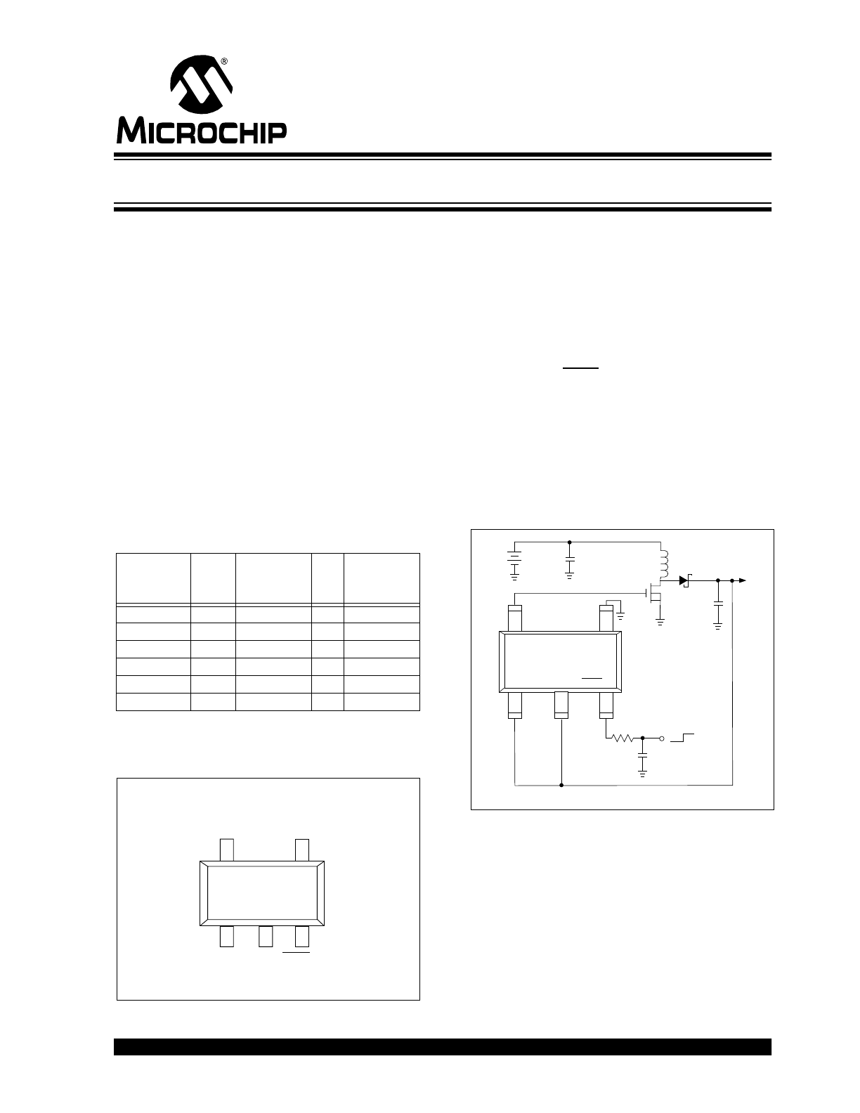
Device Selection Table
*Other
output
voltages
are
available.
Please
contact
Microchip Technology Inc. for details.
Package Type
General Description
The TC110 is a step-up (Boost) switching controller
that furnishes output currents of up to 300mA while
delivering a typical efficiency of 84%. The TC110
normally operates in pulse width modulation mode
(PWM), but automatically switches to pulse frequency
modulation (PFM) at low output loads for greater
efficiency. Supply current draw for the 100kHz version
is typically only 50
µ
A, and is reduced to less than
0.5
µ
A when the SHDN input is brought low. Regulator
operation is suspended during shutdown. The TC110
accepts input voltages from 2.0V to 10.0V, with a
guaranteed start-up voltage of 0.9V.
The TC110 is available in a small 5-Pin SOT-23A
package, occupies minimum board space and uses
small external components (the 300kHz version allows
for less than 5mm surface-mount magnetics).
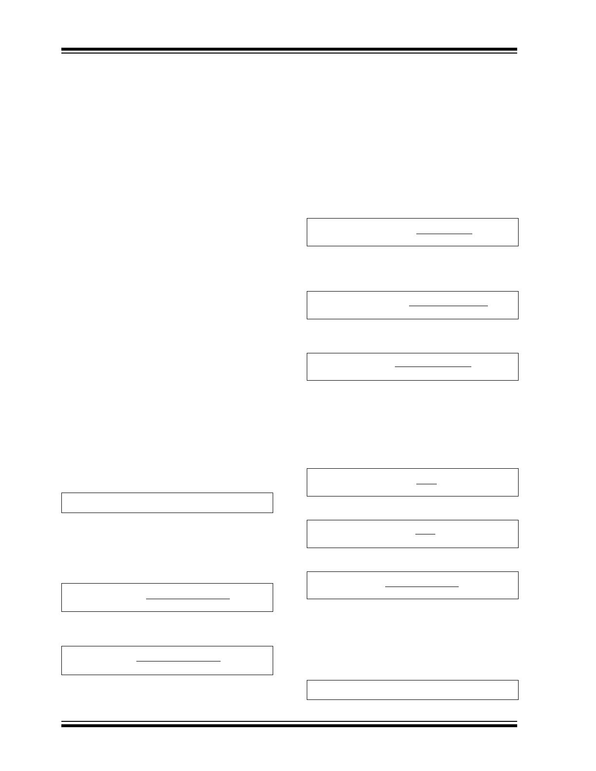
Functional Block Diagram
Part
Number
Output
Voltage
(V)*
Package
Osc.
Freq.
(kHz)
Operating
Temp.
Range
TC110501ECT
5.0
5-Pin SOT-23A
100
-40
°
C to +85
°
C
TC110331ECT
3.3
5-Pin SOT-23A
100
-40
°
C to +85
°
C
TC110301ECT
3.0
5-Pin SOT-23A
100
-40
°
C to +85
°
C
TC110503ECT
5.0
5-Pin SOT-23A
300
-40
°
C to +85
°
C
TC110333ECT
3.3
5-Pin SOT-23A
300
-40
°
C to +85
°
C
TC110303ECT
3.0
5-Pin SOT-23A
300
-40
°
C to +85
°
C
TC110
1
2
3
5
4
V
DD
EXT
GND
5-Pin SOT-23A
NOTE: 5-Pin SOT-23A is equivalent to the EIAJ SC-74A
V
OUT
SHDN/SS
5
4
TC110
1
3
2
3V to 5V Supply
SHDN/SS
V
DD
EXT
GND
IN5817
D1
47
µF
Tantalum
Si9410DY
47
µH
10
µF
Battery
3V
V
OUT
V
OUT
R
*RC Optional
C
ON
OFF
+
+
+
–
PFM/PWM Step-Up DC/DC Controller
TC110
DS21355B-page 2
2002 Microchip Technology Inc.
1.0
ELECTRICAL
CHARACTERISTICS
Absolute Maximum Ratings*
Voltage on V
DD
, V
OUT
, SHDN Pins ........ -0.3V to +12V
EXT Output Current ................................... ±100mA pk
Voltage on EXT Pin ........................-0.3V to V
DD
+0.3V
Power Dissipation.............................................150mW
Operating Temperature Range............. -40°C to +85°C
Storage Temperature Range .............. -40°C to +125°C
*Stresses above those listed under "Absolute Maximum
Ratings" may cause permanent damage to the device. These
are stress ratings only and functional operation of the device
at these or any other conditions above those indicated in the
operation sections of the specifications is not implied.
Exposure to Absolute Maximum Rating conditions for
extended periods may affect device reliability.
TC110 ELECTRICAL SPECIFICATIONS
Electrical Characteristics: Note 1, V
IN
= 0.6 x V
R
, V
DD
= V
OUT
, T
A
= 25
°
C, unless otherwise noted.
Symbol
Parameter
Min
Typ
Max
Units
Test Conditions
V
DD
Operating Supply Voltage
2.0
—
10.0
V
Note 2
V
START
Start-Up Supply Voltage
—
—
0.9
V
I
OUT
= 1mA
V
HOLD-UP
Oscillator Hold-Up Voltage
—
—
0.7
V
I
OUT
= 1mA
I
DD
Boost Mode Supply Current
—
—
—
—
—
—
120
130
180
50
50
70
190
200
280
90
100
120
µ
A
V
OUT
= SHDN = (0.95 x V
R
); f
OSC
= 300kHz; V
R
= 3.0V
V
R
= 3.3V
V
R
= 5.0V
f
OSC
= 100kHz; V
R
= 3.0V
V
R
= 3.3V
V
R
= 5.0V
I
STBY
Standby Supply Current
—
—
—
—
—
—
20
20
22
11
11
11
34
35
38
20
20
22
µ
A
V
OUT
= SHDN = (V
R
+ 0.5V); f
OSC
= 300kHz; V
R
= 3.0V
V
R
= 3.3V
V
R
= 5.0V
f
OSC
= 100kHz; V
R
= 3.0V
V
R
= 3.3V
V
R
= 5.0V
I
SHDN
Shutdown Supply Current
—
0.05
0.5
µ
A
SHDN = GND, V
O
= (V
R
x 0.95)
f
OSC
Oscillator Frequency
255
85
300
100
345
115
kHz
V
OUT
= SHDN = (0.95 x V
R
); f
OSC
= 300kHz
f
OSC
= 100kHz
V
OUT
Output Voltage
V
R
x 0.975
V
R
V
R
x 1.025
V
Note 3
DTYMAX
Maximum Duty Cycle
(PWM Mode)
—
—
92
%
V
OUT
= SHDN = 0.95 x V
R
DTYPFM
Duty Cycle (PFM Mode)
15
25
35
%
I
OUT
= 0mA
V
IH
SHDN Input Logic High
0.65
—
—
V
V
OUT
= (V
R
x 0.95)
V
IL
SHDN Input Logic Low
—
—
0.20
V
V
OUT
= (V
R
x 0.95)
REXTH
EXT ON Resistance to V
DD
—
—
—
32
29
20
47
43
29
Ω
V
OUT
= SHDN = (V
R
x 0.95); V
R
= 3.0V
V
R
= 3.3V
V
EXT
= (V
OUT
– 0.4V)
V
R
= 5.0V
REXTL
EXT ON Resistance to GND
—
—
—
20
19
13
30
27
19
Ω
V
OUT
= SHDN = (V
R
x 0.95); V
R
= 3.0V
V
R
= 3.3V
V
EXT
= 0.4V
V
R
= 5.0V
η
Efficiency
—
84
—
%
Note
1:
V
R
= 3.0V, I
OUT
= 120mA
V
R
= 3.3V, I
OUT
= 130mA
V
R
= 5.0V, I
OUT
= 200mA
2:
See Application Notes “Operating Mode” description for clarification.
3:
V
R
is the factory output voltage setting.
2002 Microchip Technology Inc.
DS21355B-page 3
TC110
2.0
PIN DESCRIPTIONS
The descriptions of the pins are listed in Table 2-1.
TABLE 2-1:
PIN FUNCTION TABLE
Pin No.
(5-Pin SOT-23A)
Symbol
Description
1
V
OUT
Internal device power and voltage sense input. This dual function input provides both feedback
voltage sensing and internal chip power. It should be connected to the regulator output. (See
Section 4.0, Applications).
2
V
DD
Power supply voltage input.
3
SHDN/SS
Shutdown input. A logic low on this input suspends device operation and supply current is
reduced to less than 0.5
µ
A. The device resumes normal operation when SHDN is again brought
high. An RC circuit connected to this input also determines the soft-start time.
4
GND
Ground terminal.
5
EXT
External switch transistor drive complimentary output. This pin drives the external switching
transistor. It may be connected to the base of the external bipolar transistor or gate of the external
N-channel MOSFET. (See Section 4.0, Applications).

TC110
DS21355B-page 4
2002 Microchip Technology Inc.
3.0
DETAILED DESCRIPTION
The TC110 is a PFM/PWM step-up DC/DC controller
for use in systems operating from two or more cells, or
in low voltage, line-powered applications. It uses PWM
as the primary modulation scheme, but automatically
converts to PFM at output duty cycles less than
approximately 25%. The conversion to PFM provides
reduced supply current, and therefore higher operating
efficiency at low loads. The TC110 uses an external
switching transistor, allowing construction of switching
regulators with maximum output currents of 300mA.
The TC110 consumes only 70
µ
A, typical, of supply
current and can be placed in a 0.5
µ
A shutdown mode
by bringing the shutdown input (SHDN) low. The
regulator remains disabled while in shutdown mode,
and normal operation resumes when SHDN is brought
high. Other features include start-up at V
IN
= 0.9V and
an externally programmable soft start time.
3.1
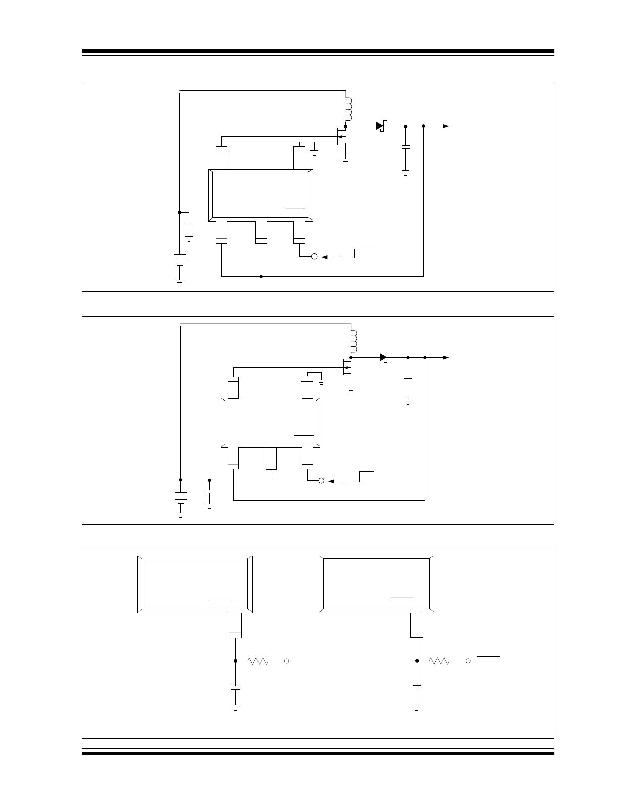
Operating Mode
The TC110 is powered by the voltage present on the
V
DD
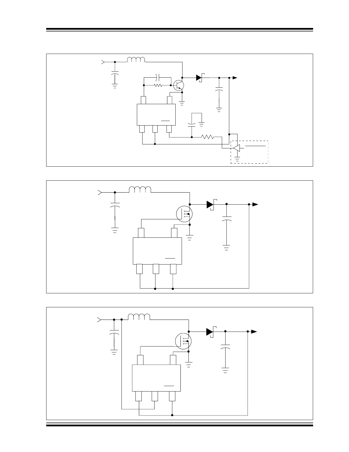
input. The applications circuits of Figure 3-1 and
Figure 3-2 show operation in the bootstrapped and
non-bootstrapped modes. In bootstrapped mode, the
TC110 is powered from the output (start-up voltage is
supplied by V
IN
through the inductor and Schottky
diode while Q1 is off). In bootstrapped mode, the
switching transistor is turned on harder because its
gate voltage is higher (due to the boost action of the
regulator), resulting in higher output current capacity.
The TC110 is powered from the input supply in the non-
bootstrapped mode. In this mode, the supply current to
the TC110 is minimized. However, the drive applied to
the gate of the switching transistor swings from the
input supply level to ground, so the transistor’s ON
resistance increases at low input voltages. Overall
efficiency is increased since supply current is reduced,
and less energy is consumed charging and discharging
the gate of the MOSFET. While the TC110 is guaran-
teed to start up at 0.9V the device performs to
specifications at 2.0V and higher.
3.2
Low Power Shutdown Mode
The TC110 enters a low power shutdown mode when
SHDN is brought low. While in shutdown, the oscillator
is disabled and the output switch (internal or external)
is shut off. Normal regulator operation resumes when
SHDN is brought high. SHDN may be tied to the input
supply if not used.
Note:
Because the TC110 uses an external diode,
a leakage path between the input voltage
and the output node (through the inductor
and diode) exists while the regulator is in
shutdown. Care must be taken in system
design to assure the input supply is isolated
from the load during shutdown.
3.3
Soft Start
Soft start allows the output voltage to gradually ramp
from 0V to rated output value during start-up. This
action minimizes (or eliminates) overshoot, and in
general,
reduces
stress
on
circuit
components.
Figure 3-3 shows the circuit required to implement soft
start (values of 470K and 0.1
µ
F for R
SS
and C
SS
,
respectively, are adequate for most applications).
3.4
Input Bypass Capacitors
Using an input bypass capacitor reduces peak current
transients drawn from the input supply and reduces the
switching noise generated by the regulator. The source
impedance of the input supply determines the size of
the capacitor that should be used.
2002 Microchip Technology Inc.
DS21355B-page 5
TC110
FIGURE 3-1:
BOOTSTRAPPED OPERATION
FIGURE 3-2:
NON-BOOTSTRAPPED OPERATION
FIGURE 3-3:
SOFT START/SHUTDOWN CIRCUIT
5
4
TC110XX
1
3
2
V
OUT
EXT
GND
D1
IN5817
C2
47
µF
L1
100
µH
V
OUT
OFF ON
n
MTP3055EL
C1
33
µF
V
IN
SHDN
V
DD
+
–
5
4
TC110XX
1
3
2
V
OUT
EXT
GND
D1
IN5817
C2
47
µF
L1
100
µH
V
OUT
OFF ON
n
MTP3055EL
C1
33
µF
V
IN
SHDN
V
DD
+
–
TC110XX
3
SHDN/SS
C
SS
0.1
µF
SHDN
R
SS
470K
V
IN
TC110XX
3
SHDN/SS
C
SS
0.1
µF
R
SS
470K
Shutdown Used
Shutdown Not Used
TC110
DS21355B-page 6
2002 Microchip Technology Inc.
3.5
Output Capacitor
The effective series resistance of the output capacitor
directly affects the amplitude of the output voltage
ripple. (The product of the peak inductor current and
the ESR determines output ripple amplitude.) There-
fore, a capacitor with the lowest possible ESR should
be selected. Smaller capacitors are acceptable for light
loads or in applications where ripple is not a concern.
The Sprague 595D series of tantalum capacitors are
among the smallest of all low ESR surface mount
capacitors
available.
Table 4-1
lists
suggested
components and suppliers.
3.6
Inductor Selection
Selecting the proper inductor value is a trade-off
between physical size and power conversion require-
ments. Lower value inductors cost less, but result in
higher ripple current and core losses. They are also
more prone to saturate since the coil current ramps
faster and could overshoot the desired peak value. This
not only reduces efficiency, but could also cause the
current rating of the external components to be
exceeded. Larger inductor values reduce both ripple
current and core losses, but are larger in physical size
and tend to increase the start-up time slightly.
A 22
µ
H inductor is recommended for the 300kHz
versions and a 47
µ
H inductor is recommended for the
100kHz versions. Inductors with a ferrite core (or
equivalent) are
also
recommended. For highest
efficiency, use inductors with a low DC resistance (less
than 20 m
Ω
).
The inductor value directly affects the output ripple
voltage. Equation 3-3 is derived as shown below, and
can be used to calculate an inductor value, given the
required output ripple voltage and output capacitor
series resistance:
EQUATION 3-1:
where ESR is the equivalent series resistance of the
output filter capacitor, and V
RIPPLE
is in volts.
Expressing di in terms of switch ON resistance and
time:
EQUATION 3-2:
Solving for L:
EQUATION 3-3:
Care must be taken to ensure the inductor can handle
peak switching currents, which can be several times
load currents. Exceeding rated peak current will result
in core saturation and loss of inductance. The inductor
should be selected to withstand currents greater than
I
PK
(Equation 3-10) without saturating.
Calculating the peak inductor current is straightforward.
Inductor current consists of an AC (sawtooth) current
centered on an average DC current (i.e., input current).
Equation 3-6 calculates the average DC current. Note
that minimum input voltage and maximum load current
values should be used:
EQUATION 3-4:
Re-writing in terms of input and output currents and
voltages:
EQUATION 3-5:
Solving for input curent:
EQUATION 3-6:
The sawtooth current is centered on the DC current
level; swinging equally above and below the DC current
calculated in Equation 3-6. The peak inductor current is
the sum of the DC current plus half the AC current.
Note that minimum input voltage should be used when
calculating the AC inductor current (Equation 3-9).
EQUATION 3-7:
EQUATION 3-8:
EQUATION 3-9:
where: V
SW
= V
CESAT
of the switch (note if a CMOS
switch is used substitute V
CESAT
for r
DS
ON
x I
IN
)
Combining the DC current calculated in Equation 3-6,
with half the peak AC current calculated in Equation 3-
9, the peak inductor current is given by:
EQUATION 3-10:
V
RIPPLE
≈
ESR(di)
V
RIPPLE
≈
ESR [(V
IN
– V
SW
)t
ON
]
L
≈
ESR [(V
IN
– V
SW
)t
ON
]
V
RIPPLE
L
=
Output Power
Efficiency
Input Power
(V
OUT
MAX
) (I
OUT
MAX
)
Efficiency
(V
IN
MIN
) (I
IN
MAX
) =
(V
OUT
MAX
) (I
OUT
MAX
)
(Efficiency)(V
IN
MAX
)
I
IN
MAX
=
=
L(di)
dt
V
=
V(dt)
dt
di
[(V
IN
MIN
– V
SW
)t
ON
]
L
di =
I
PK
= I
IN
MAX
+ 0.5(di)

2002 Microchip Technology Inc.
DS21355B-page 7
TC110
3.7
Output Diode
For best results, use a Schottky diode such as the
MA735, 1N5817, MBR0520L or equivalent. Connect
the diode between the FB (or SENSE) input as close to
the IC as possible. Do not use ordinary rectifier diodes
since the higher threshold voltages reduce efficiency.
3.8
External Switching Transistor
Selection
The EXT output is designed to directly drive an
N-channel MOSFET or NPN bipolar transistor. N-
channel
MOSFETs
afford
the
highest
efficiency
because they do not draw continuous gate drive
current, but are typically more expensive than bipolar
transistors. If using an N-channel MOSFET, the gate
should be connected directly to the EXT output as
shown in Figure 3-1 and Figure 3-1. EXT is a compli-
mentary output with a maximum ON resistances of 43
Ω
to V
DD
when high and 27
Ω
to ground when low. Peak
currents should be kept below 10mA.
When selecting an N-channel MOSFET, there are three
important parameters to consider: total gate charge
(Qg); ON resistance (r
DS
ON
) and reverse transfer
capacitance (CRSS). Qg is a measure of the total gate
capacitance that will ultimately load the EXT output.
Too high a Qg can reduce the slew rate of the EXT
output sufficiently to grossly lower operating efficiency.
Transistors with typical Qg data sheet values of 50nC
or less can be used. For example, the Si9410DY has a
Qg (typ) of 17nC @ V
GS
= 5V. This equates to a gate
current of:
I
GATE
MAX
= f
MAX
x Qg = 115kHz x 17nC = 2mA
The two most significant losses in the N-channel
MOSFET are switching loss and I
2
R loss. To minimize
these, a transistor with low r
DS
ON
and low CRSS should
be used.
Bipolar NPN transistors can be used, but care must be
taken when determining base current drive. Too little
current will not fully turn the transistor on, and result in
unstable regulator operation and low efficiency. Too
high a base drive causes excessive power dissipation
in the transistor and increase switching time due to
over-saturation. For peak efficiency, make R
B
as large
as possible, but still guaranteeing the switching transis-
tor is completely saturated when the minimum value of
h
FE
is used.
3.9
Board Layout Guidelines
As with all inductive switching regulators, the TC110
generates fast switching waveforms which radiate
noise. Interconnecting lead lengths should be mini-
mized to keep stray capacitance, trace resistance and
radiated noise as low as possible. In addition, the GND
pin, input bypass capacitor and output filter capacitor
ground leads should be connected to a single point.
The input capacitor should be placed as close to power
and ground pins of the TC110 as possible.

TC110
DS21355B-page 8
2002 Microchip Technology Inc.
4.0
APPLICATIONS
4.1
Circuit Examples
Figure 4-1 shows a TC110 operating as a 100kHz
bootstrapped regulator with soft start. This circuit uses
an NPN switching transistor (Zetex FZT690B) that has
an h
FE
of 400 and V
CESAT
of 100 mV at I
C
= 1A. Other
high beta transistors can be used, but the values of R
B
and C
B
may need adjustment if h
FE
is significantly
different from that of the FZT690B.
Figure 4-2 and Figure 4-3 both utilize an N-channel
switching transistor (Silconix Si9410DY). This transistor
is a member of the Littlefoot
TM
family of small outline
MOSFETs. The circuit of Figure 4-2 operates in
bootstrapped mode, while the circuit of Figure 4-3
operates in non-bootstrapped mode.
TABLE 4-1:
SUGGESTED COMPONENTS AND SUPPLIERS
Type
Inductors
Capacitors
Diodes
Transistors
Surface Mount
Sumida
CD54 Series (300kHz)
CD75 (100kHz)
Coiltronics
CTX Series
Matsuo
267 Series
Sprague
595D Series
Nichicon
F93 Series
Nihon
EC10 Series
Matsushita
MA735 Series
N-channel
Silconix
Si9410DY
ON Semiconductor
MTP3055EL
MTD20N03
Through-Hole
Sumida
RCH855 Series
RCH110 Series
Renco
RL1284-12
Sanyo
OS-CON Series
Nichicon
PL Series
ON Semiconductor
1N5817 - 1N5822
NPN
Zetex
ZTX694B
2002 Microchip Technology Inc.
DS21355B-page 9
TC110
FIGURE 4-1:
100kHz BOOTSTRAPPED REGULATOR WITH SOFT START USING
A BIPOLAR TRANSISTOR
FIGURE 4-2:
300kHz BOOTSTRAPPED, N-CHANNEL TRANSISTOR
FIGURE 4-3:
300kHz NON-BOOTSTRAPPED, N-CHANNEL TRANSISTOR
TC110301
C
IN
10
µF/16V
V
IN
EXT
V
OUT
V
OUT
D1
Matsushita
MA737
1
2
3
4
5
Q1
FZT690BCT
RB
1K
CB
10nF
Ceramic
L1
47
µH
Sumida CD75
C
OUT
47
µF, 10V
Tant.
SHUTDOWN
(Optional)
R
SS
470K
C
SS
0.1
µF
Ceramic
TC110301
GND
V
DD
SHDN/SS
1
2
3
4
5
C
IN
10
µF/16V
V
IN
EXT
V
OUT
V
OUT
D1
ON Semiconductor
MBR0520L
Q1
Silconix
Si9410DY
L1
22
µH
Sumida CD54
C
OUT
47
µF, 16V
Tant.
GND
V
DD
SHDN/SS
TC110303
1
2
3
4
5
C
IN
10
µF/16V
V
IN
EXT
V
OUT
V
OUT
D1
ON Semiconductor
MBR0520L
Q1
Silconix
Si9410DY
L1
22
µH
Sumida CD54
C
OUT
47
µF, 16V
Tant.
GND
V
DD
SHDN/SS
TC110303
TC110
DS21355B-page 10
2002 Microchip Technology Inc.
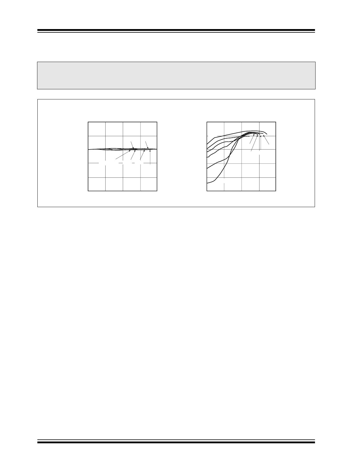
5.0
TYPICAL CHARACTERISTICS
(Unless Otherwise Specified, All Parts Are Measured At Temperature = 25°C)
Note:
The graphs and tables provided following this note are a statistical summary based on a limited number of
samples and are provided for informational purposes only. The performance characteristics listed herein are
not tested or guaranteed. In some graphs or tables, the data presented may be outside the specified
operating range (e.g., outside specified power supply range) and therefore outside the warranted range.
OUTPUT CURRENT I
OUT
(mA)
3.0
0.1
1
10
100
1000
3.1
3.2
3.3
3.4
3.5
OUTPUT VOLTAGE (V
OUT
) (V)
L = 22
µH, CL = 94µF (Tantalum)
V
IN
= 0.9V
1.2V
1.8V
1.5V
2.0V
2.7V
Output Voltage vs. Output Current
TC110 (300kHz, 3.3V)
OUTPUT CURRENT I
OUT
(mA)
L = 22
µH, CL = 94µF (Tantalum)
Efficiency vs. Output Current
TC110 (300kHz, 3.3V)
0
0.1
1
10
100
1000
20
40
60
80
100
E
FFICIENCY
(%
)
V
IN
= 0.9V
1.2V
1.8V
1.5V
2.0V
2.7V
2002 Microchip Technology Inc.
DS21355B-page 1
TC110
Features
• Assured Start-up at 0.9V
• 50
µ
A (Typ) Supply Current (f
OSC
= 100kHz)
• 300mA Output Current @ V
IN
≥
2.7V
• 0.5
µ
A Shutdown Mode
• 100kHz and 300kHz Switching Frequency
Options
• Programmable Soft-Start
• 84% Typical Efficiency
• Small Package: 5-Pin SOT-23A
Applications
• Palmtops
• Battery-Operated Systems
• Positive LCD Bias Generators
• Portable Communicators
Device Selection Table
*Other
output
voltages
are
available.
Please
contact
Microchip Technology Inc. for details.
Package Type
General Description
The TC110 is a step-up (Boost) switching controller
that furnishes output currents of up to 300mA while
delivering a typical efficiency of 84%. The TC110
normally operates in pulse width modulation mode
(PWM), but automatically switches to pulse frequency
modulation (PFM) at low output loads for greater
efficiency. Supply current draw for the 100kHz version
is typically only 50
µ
A, and is reduced to less than
0.5
µ
A when the SHDN input is brought low. Regulator
operation is suspended during shutdown. The TC110
accepts input voltages from 2.0V to 10.0V, with a
guaranteed start-up voltage of 0.9V.
The TC110 is available in a small 5-Pin SOT-23A
package, occupies minimum board space and uses
small external components (the 300kHz version allows
for less than 5mm surface-mount magnetics).
Functional Block Diagram
Part
Number
Output
Voltage
(V)*
Package
Osc.
Freq.
(kHz)
Operating
Temp.
Range
TC110501ECT
5.0
5-Pin SOT-23A
100
-40
°
C to +85
°
C
TC110331ECT
3.3
5-Pin SOT-23A
100
-40
°
C to +85
°
C
TC110301ECT
3.0
5-Pin SOT-23A
100
-40
°
C to +85
°
C
TC110503ECT
5.0
5-Pin SOT-23A
300
-40
°
C to +85
°
C
TC110333ECT
3.3
5-Pin SOT-23A
300
-40
°
C to +85
°
C
TC110303ECT
3.0
5-Pin SOT-23A
300
-40
°
C to +85
°
C
TC110
1
2
3
5
4
V
DD
EXT
GND
5-Pin SOT-23A
NOTE: 5-Pin SOT-23A is equivalent to the EIAJ SC-74A
V
OUT
SHDN/SS
5
4
TC110
1
3
2
3V to 5V Supply
SHDN/SS
V
DD
EXT
GND
IN5817
D1
47
µF
Tantalum
Si9410DY
47
µH
10
µF
Battery
3V
V
OUT
V
OUT
R
*RC Optional
C
ON
OFF
+
+
+
–
PFM/PWM Step-Up DC/DC Controller
TC110
DS21355B-page 2
2002 Microchip Technology Inc.
1.0
ELECTRICAL
CHARACTERISTICS
Absolute Maximum Ratings*
Voltage on V
DD
, V
OUT
, SHDN Pins ........ -0.3V to +12V
EXT Output Current ................................... ±100mA pk
Voltage on EXT Pin ........................-0.3V to V
DD
+0.3V
Power Dissipation.............................................150mW
Operating Temperature Range............. -40°C to +85°C
Storage Temperature Range .............. -40°C to +125°C
*Stresses above those listed under "Absolute Maximum
Ratings" may cause permanent damage to the device. These
are stress ratings only and functional operation of the device
at these or any other conditions above those indicated in the
operation sections of the specifications is not implied.
Exposure to Absolute Maximum Rating conditions for
extended periods may affect device reliability.
TC110 ELECTRICAL SPECIFICATIONS
Electrical Characteristics: Note 1, V
IN
= 0.6 x V
R
, V
DD
= V
OUT
, T
A
= 25
°
C, unless otherwise noted.
Symbol
Parameter
Min
Typ
Max
Units
Test Conditions
V
DD
Operating Supply Voltage
2.0
—
10.0
V
Note 2
V
START
Start-Up Supply Voltage
—
—
0.9
V
I
OUT
= 1mA
V
HOLD-UP
Oscillator Hold-Up Voltage
—
—
0.7
V
I
OUT
= 1mA
I
DD
Boost Mode Supply Current
—
—
—
—
—
—
120
130
180
50
50
70
190
200
280
90
100
120
µ
A
V
OUT
= SHDN = (0.95 x V
R
); f
OSC
= 300kHz; V
R
= 3.0V
V
R
= 3.3V
V
R
= 5.0V
f
OSC
= 100kHz; V
R
= 3.0V
V
R
= 3.3V
V
R
= 5.0V
I
STBY
Standby Supply Current
—
—
—
—
—
—
20
20
22
11
11
11
34
35
38
20
20
22
µ
A
V
OUT
= SHDN = (V
R
+ 0.5V); f
OSC
= 300kHz; V
R
= 3.0V
V
R
= 3.3V
V
R
= 5.0V
f
OSC
= 100kHz; V
R
= 3.0V
V
R
= 3.3V
V
R
= 5.0V
I
SHDN
Shutdown Supply Current
—
0.05
0.5
µ
A
SHDN = GND, V
O
= (V
R
x 0.95)
f
OSC
Oscillator Frequency
255
85
300
100
345
115
kHz
V
OUT
= SHDN = (0.95 x V
R
); f
OSC
= 300kHz
f
OSC
= 100kHz
V
OUT
Output Voltage
V
R
x 0.975
V
R
V
R
x 1.025
V
Note 3
DTYMAX
Maximum Duty Cycle
(PWM Mode)
—
—
92
%
V
OUT
= SHDN = 0.95 x V
R
DTYPFM
Duty Cycle (PFM Mode)
15
25
35
%
I
OUT
= 0mA
V
IH
SHDN Input Logic High
0.65
—
—
V
V
OUT
= (V
R
x 0.95)
V
IL
SHDN Input Logic Low
—
—
0.20
V
V
OUT
= (V
R
x 0.95)
REXTH
EXT ON Resistance to V
DD
—
—
—
32
29
20
47
43
29
Ω
V
OUT
= SHDN = (V
R
x 0.95); V
R
= 3.0V
V
R
= 3.3V
V
EXT
= (V
OUT
– 0.4V)
V
R
= 5.0V
REXTL
EXT ON Resistance to GND
—
—
—
20
19
13
30
27
19
Ω
V
OUT
= SHDN = (V
R
x 0.95); V
R
= 3.0V
V
R
= 3.3V
V
EXT
= 0.4V
V
R
= 5.0V
η
Efficiency
—
84
—
%
Note
1:
V
R
= 3.0V, I
OUT
= 120mA
V
R
= 3.3V, I
OUT
= 130mA
V
R
= 5.0V, I
OUT
= 200mA
2:
See Application Notes “Operating Mode” description for clarification.
3:
V
R
is the factory output voltage setting.
2002 Microchip Technology Inc.
DS21355B-page 3
TC110
2.0
PIN DESCRIPTIONS
The descriptions of the pins are listed in Table 2-1.
TABLE 2-1:
PIN FUNCTION TABLE
Pin No.
(5-Pin SOT-23A)
Symbol
Description
1
V
OUT
Internal device power and voltage sense input. This dual function input provides both feedback
voltage sensing and internal chip power. It should be connected to the regulator output. (See
Section 4.0, Applications).
2
V
DD
Power supply voltage input.
3
SHDN/SS
Shutdown input. A logic low on this input suspends device operation and supply current is
reduced to less than 0.5
µ
A. The device resumes normal operation when SHDN is again brought
high. An RC circuit connected to this input also determines the soft-start time.
4
GND
Ground terminal.
5
EXT
External switch transistor drive complimentary output. This pin drives the external switching
transistor. It may be connected to the base of the external bipolar transistor or gate of the external
N-channel MOSFET. (See Section 4.0, Applications).
TC110
DS21355B-page 4
2002 Microchip Technology Inc.
3.0
DETAILED DESCRIPTION
The TC110 is a PFM/PWM step-up DC/DC controller
for use in systems operating from two or more cells, or
in low voltage, line-powered applications. It uses PWM
as the primary modulation scheme, but automatically
converts to PFM at output duty cycles less than
approximately 25%. The conversion to PFM provides
reduced supply current, and therefore higher operating
efficiency at low loads. The TC110 uses an external
switching transistor, allowing construction of switching
regulators with maximum output currents of 300mA.
The TC110 consumes only 70
µ
A, typical, of supply
current and can be placed in a 0.5
µ
A shutdown mode
by bringing the shutdown input (SHDN) low. The
regulator remains disabled while in shutdown mode,
and normal operation resumes when SHDN is brought
high. Other features include start-up at V
IN
= 0.9V and
an externally programmable soft start time.
3.1
Operating Mode
The TC110 is powered by the voltage present on the
V
DD
input. The applications circuits of Figure 3-1 and
Figure 3-2 show operation in the bootstrapped and
non-bootstrapped modes. In bootstrapped mode, the
TC110 is powered from the output (start-up voltage is
supplied by V
IN
through the inductor and Schottky
diode while Q1 is off). In bootstrapped mode, the
switching transistor is turned on harder because its
gate voltage is higher (due to the boost action of the
regulator), resulting in higher output current capacity.
The TC110 is powered from the input supply in the non-
bootstrapped mode. In this mode, the supply current to
the TC110 is minimized. However, the drive applied to
the gate of the switching transistor swings from the
input supply level to ground, so the transistor’s ON
resistance increases at low input voltages. Overall
efficiency is increased since supply current is reduced,
and less energy is consumed charging and discharging
the gate of the MOSFET. While the TC110 is guaran-
teed to start up at 0.9V the device performs to
specifications at 2.0V and higher.
3.2
Low Power Shutdown Mode
The TC110 enters a low power shutdown mode when
SHDN is brought low. While in shutdown, the oscillator
is disabled and the output switch (internal or external)
is shut off. Normal regulator operation resumes when
SHDN is brought high. SHDN may be tied to the input
supply if not used.
Note:
Because the TC110 uses an external diode,
a leakage path between the input voltage
and the output node (through the inductor
and diode) exists while the regulator is in
shutdown. Care must be taken in system
design to assure the input supply is isolated
from the load during shutdown.
3.3
Soft Start
Soft start allows the output voltage to gradually ramp
from 0V to rated output value during start-up. This
action minimizes (or eliminates) overshoot, and in
general,
reduces
stress
on
circuit
components.
Figure 3-3 shows the circuit required to implement soft
start (values of 470K and 0.1
µ
F for R
SS
and C
SS
,
respectively, are adequate for most applications).
3.4
Input Bypass Capacitors
Using an input bypass capacitor reduces peak current
transients drawn from the input supply and reduces the
switching noise generated by the regulator. The source
impedance of the input supply determines the size of
the capacitor that should be used.
2002 Microchip Technology Inc.
DS21355B-page 5
TC110
FIGURE 3-1:
BOOTSTRAPPED OPERATION
FIGURE 3-2:
NON-BOOTSTRAPPED OPERATION
FIGURE 3-3:
SOFT START/SHUTDOWN CIRCUIT
5
4
TC110XX
1
3
2
V
OUT
EXT
GND
D1
IN5817
C2
47
µF
L1
100
µH
V
OUT
OFF ON
n
MTP3055EL
C1
33
µF
V
IN
SHDN
V
DD
+
–
5
4
TC110XX
1
3
2
V
OUT
EXT
GND
D1
IN5817
C2
47
µF
L1
100
µH
V
OUT
OFF ON
n
MTP3055EL
C1
33
µF
V
IN
SHDN
V
DD
+
–
TC110XX
3
SHDN/SS
C
SS
0.1
µF
SHDN
R
SS
470K
V
IN
TC110XX
3
SHDN/SS
C
SS
0.1
µF
R
SS
470K
Shutdown Used
Shutdown Not Used
TC110
DS21355B-page 6
2002 Microchip Technology Inc.
3.5
Output Capacitor
The effective series resistance of the output capacitor
directly affects the amplitude of the output voltage
ripple. (The product of the peak inductor current and
the ESR determines output ripple amplitude.) There-
fore, a capacitor with the lowest possible ESR should
be selected. Smaller capacitors are acceptable for light
loads or in applications where ripple is not a concern.
The Sprague 595D series of tantalum capacitors are
among the smallest of all low ESR surface mount
capacitors
available.
Table 4-1
lists
suggested
components and suppliers.
3.6
Inductor Selection
Selecting the proper inductor value is a trade-off
between physical size and power conversion require-
ments. Lower value inductors cost less, but result in
higher ripple current and core losses. They are also
more prone to saturate since the coil current ramps
faster and could overshoot the desired peak value. This
not only reduces efficiency, but could also cause the
current rating of the external components to be
exceeded. Larger inductor values reduce both ripple
current and core losses, but are larger in physical size
and tend to increase the start-up time slightly.
A 22
µ
H inductor is recommended for the 300kHz
versions and a 47
µ
H inductor is recommended for the
100kHz versions. Inductors with a ferrite core (or
equivalent) are
also
recommended. For highest
efficiency, use inductors with a low DC resistance (less
than 20 m
Ω
).
The inductor value directly affects the output ripple
voltage. Equation 3-3 is derived as shown below, and
can be used to calculate an inductor value, given the
required output ripple voltage and output capacitor
series resistance:
EQUATION 3-1:
where ESR is the equivalent series resistance of the
output filter capacitor, and V
RIPPLE
is in volts.
Expressing di in terms of switch ON resistance and
time:
EQUATION 3-2:
Solving for L:
EQUATION 3-3:
Care must be taken to ensure the inductor can handle
peak switching currents, which can be several times
load currents. Exceeding rated peak current will result
in core saturation and loss of inductance. The inductor
should be selected to withstand currents greater than
I
PK
(Equation 3-10) without saturating.
Calculating the peak inductor current is straightforward.
Inductor current consists of an AC (sawtooth) current
centered on an average DC current (i.e., input current).
Equation 3-6 calculates the average DC current. Note
that minimum input voltage and maximum load current
values should be used:
EQUATION 3-4:
Re-writing in terms of input and output currents and
voltages:
EQUATION 3-5:
Solving for input curent:
EQUATION 3-6:
The sawtooth current is centered on the DC current
level; swinging equally above and below the DC current
calculated in Equation 3-6. The peak inductor current is
the sum of the DC current plus half the AC current.
Note that minimum input voltage should be used when
calculating the AC inductor current (Equation 3-9).
EQUATION 3-7:
EQUATION 3-8:
EQUATION 3-9:
where: V
SW
= V
CESAT
of the switch (note if a CMOS
switch is used substitute V
CESAT
for r
DS
ON
x I
IN
)
Combining the DC current calculated in Equation 3-6,
with half the peak AC current calculated in Equation 3-
9, the peak inductor current is given by:
EQUATION 3-10:
V
RIPPLE
≈
ESR(di)
V
RIPPLE
≈
ESR [(V
IN
– V
SW
)t
ON
]
L
≈
ESR [(V
IN
– V
SW
)t
ON
]
V
RIPPLE
L
=
Output Power
Efficiency
Input Power
(V
OUT
MAX
) (I
OUT
MAX
)
Efficiency
(V
IN
MIN
) (I
IN
MAX
) =
(V
OUT
MAX
) (I
OUT
MAX
)
(Efficiency)(V
IN
MAX
)
I
IN
MAX
=
=
L(di)
dt
V
=
V(dt)
dt
di
[(V
IN
MIN
– V
SW
)t
ON
]
L
di =
I
PK
= I
IN
MAX
+ 0.5(di)
2002 Microchip Technology Inc.
DS21355B-page 7
TC110
3.7
Output Diode
For best results, use a Schottky diode such as the
MA735, 1N5817, MBR0520L or equivalent. Connect
the diode between the FB (or SENSE) input as close to
the IC as possible. Do not use ordinary rectifier diodes
since the higher threshold voltages reduce efficiency.
3.8
External Switching Transistor
Selection
The EXT output is designed to directly drive an
N-channel MOSFET or NPN bipolar transistor. N-
channel
MOSFETs
afford
the
highest
efficiency
because they do not draw continuous gate drive
current, but are typically more expensive than bipolar
transistors. If using an N-channel MOSFET, the gate
should be connected directly to the EXT output as
shown in Figure 3-1 and Figure 3-1. EXT is a compli-
mentary output with a maximum ON resistances of 43
Ω
to V
DD
when high and 27
Ω
to ground when low. Peak
currents should be kept below 10mA.
When selecting an N-channel MOSFET, there are three
important parameters to consider: total gate charge
(Qg); ON resistance (r
DS
ON
) and reverse transfer
capacitance (CRSS). Qg is a measure of the total gate
capacitance that will ultimately load the EXT output.
Too high a Qg can reduce the slew rate of the EXT
output sufficiently to grossly lower operating efficiency.
Transistors with typical Qg data sheet values of 50nC
or less can be used. For example, the Si9410DY has a
Qg (typ) of 17nC @ V
GS
= 5V. This equates to a gate
current of:
I
GATE
MAX
= f
MAX
x Qg = 115kHz x 17nC = 2mA
The two most significant losses in the N-channel
MOSFET are switching loss and I
2
R loss. To minimize
these, a transistor with low r
DS
ON
and low CRSS should
be used.
Bipolar NPN transistors can be used, but care must be
taken when determining base current drive. Too little
current will not fully turn the transistor on, and result in
unstable regulator operation and low efficiency. Too
high a base drive causes excessive power dissipation
in the transistor and increase switching time due to
over-saturation. For peak efficiency, make R
B
as large
as possible, but still guaranteeing the switching transis-
tor is completely saturated when the minimum value of
h
FE
is used.
3.9
Board Layout Guidelines
As with all inductive switching regulators, the TC110
generates fast switching waveforms which radiate
noise. Interconnecting lead lengths should be mini-
mized to keep stray capacitance, trace resistance and
radiated noise as low as possible. In addition, the GND
pin, input bypass capacitor and output filter capacitor
ground leads should be connected to a single point.
The input capacitor should be placed as close to power
and ground pins of the TC110 as possible.
TC110
DS21355B-page 8
2002 Microchip Technology Inc.
4.0
APPLICATIONS
4.1
Circuit Examples
Figure 4-1 shows a TC110 operating as a 100kHz
bootstrapped regulator with soft start. This circuit uses
an NPN switching transistor (Zetex FZT690B) that has
an h
FE
of 400 and V
CESAT
of 100 mV at I
C
= 1A. Other
high beta transistors can be used, but the values of R
B
and C
B
may need adjustment if h
FE
is significantly
different from that of the FZT690B.
Figure 4-2 and Figure 4-3 both utilize an N-channel
switching transistor (Silconix Si9410DY). This transistor
is a member of the Littlefoot
TM
family of small outline
MOSFETs. The circuit of Figure 4-2 operates in
bootstrapped mode, while the circuit of Figure 4-3
operates in non-bootstrapped mode.
TABLE 4-1:
SUGGESTED COMPONENTS AND SUPPLIERS
Type
Inductors
Capacitors
Diodes
Transistors
Surface Mount
Sumida
CD54 Series (300kHz)
CD75 (100kHz)
Coiltronics
CTX Series
Matsuo
267 Series
Sprague
595D Series
Nichicon
F93 Series
Nihon
EC10 Series
Matsushita
MA735 Series
N-channel
Silconix
Si9410DY
ON Semiconductor
MTP3055EL
MTD20N03
Through-Hole
Sumida
RCH855 Series
RCH110 Series
Renco
RL1284-12
Sanyo
OS-CON Series
Nichicon
PL Series
ON Semiconductor
1N5817 - 1N5822
NPN
Zetex
ZTX694B
2002 Microchip Technology Inc.
DS21355B-page 9
TC110
FIGURE 4-1:
100kHz BOOTSTRAPPED REGULATOR WITH SOFT START USING
A BIPOLAR TRANSISTOR
FIGURE 4-2:
300kHz BOOTSTRAPPED, N-CHANNEL TRANSISTOR
FIGURE 4-3:
300kHz NON-BOOTSTRAPPED, N-CHANNEL TRANSISTOR
TC110301
C
IN
10
µF/16V
V
IN
EXT
V
OUT
V
OUT
D1
Matsushita
MA737
1
2
3
4
5
Q1
FZT690BCT
RB
1K
CB
10nF
Ceramic
L1
47
µH
Sumida CD75
C
OUT
47
µF, 10V
Tant.
SHUTDOWN
(Optional)
R
SS
470K
C
SS
0.1
µF
Ceramic
TC110301
GND
V
DD
SHDN/SS
1
2
3
4
5
C
IN
10
µF/16V
V
IN
EXT
V
OUT
V
OUT
D1
ON Semiconductor
MBR0520L
Q1
Silconix
Si9410DY
L1
22
µH
Sumida CD54
C
OUT
47
µF, 16V
Tant.
GND
V
DD
SHDN/SS
TC110303
1
2
3
4
5
C
IN
10
µF/16V
V
IN
EXT
V
OUT
V
OUT
D1
ON Semiconductor
MBR0520L
Q1
Silconix
Si9410DY
L1
22
µH
Sumida CD54
C
OUT
47
µF, 16V
Tant.
GND
V
DD
SHDN/SS
TC110303
TC110
DS21355B-page 10
2002 Microchip Technology Inc.
5.0
TYPICAL CHARACTERISTICS
(Unless Otherwise Specified, All Parts Are Measured At Temperature = 25°C)
Note:
The graphs and tables provided following this note are a statistical summary based on a limited number of
samples and are provided for informational purposes only. The performance characteristics listed herein are
not tested or guaranteed. In some graphs or tables, the data presented may be outside the specified
operating range (e.g., outside specified power supply range) and therefore outside the warranted range.
OUTPUT CURRENT I
OUT
(mA)
3.0
0.1
1
10
100
1000
3.1
3.2
3.3
3.4
3.5
OUTPUT VOLTAGE (V
OUT
) (V)
L = 22
µH, CL = 94µF (Tantalum)
V
IN
= 0.9V
1.2V
1.8V
1.5V
2.0V
2.7V
Output Voltage vs. Output Current
TC110 (300kHz, 3.3V)
OUTPUT CURRENT I
OUT
(mA)
L = 22
µH, CL = 94µF (Tantalum)
Efficiency vs. Output Current
TC110 (300kHz, 3.3V)
0
0.1
1
10
100
1000
20
40
60
80
100
E
FFICIENCY
(%
)
V
IN
= 0.9V
1.2V
1.8V
1.5V
2.0V
2.7V