
2015-2016 Microchip Technology Inc.
DS20005386B-page 1
PAC1710/20
Features
• Single and Dual High-Side Current Sensor
- Current measurement is integrated over 2.5 ms
to 2.6 seconds with up to 11-bit resolution
- 1% current measurement accuracy in
positive range
- Measures V
SOURCE
voltages
• Calculates Power
• V
SOURCE
Voltage Range 0V to 40V
• Bidirectional Current Sensing
• Auto-Zero Input Offset Voltage
• Digital Averaging
- Adjustable sampling time and resolution
• 5 µA Typical Standby Current
• Programmable Sense Voltage Range
- ±10 mV, ±20 mV, ±40 mV, and ±80 mV
• Power Supply Range 3.0V to 5.5V
• Wide Temperature Operating Range: -40°C to
+85°C
• ALERT Output for Voltage and Current out of
Limit Transients Between Sampling Interval
• SMBus 2.0 Communications Interface
- Block Read and Block Write
- Address selectable by resistor decode
• Sample Time Configurable from 2.5 ms to 320 ms
- With averaging effective sampling times up to
2.6 seconds
• 10-Lead 3 x 3 mm VDFN package
Applications
• Notebook and Desktop Computers
• Industrial
• Power Management Systems
• Embedded Applications
• Servers
Description
The PAC1710/20 are single and dual high-side
bidirectional current sensing monitors with precision
voltage measurement capabilities.
Each sensor
measures the voltage developed across an external
sense resistor to represent the high-side current of a
battery or voltage regulator. The PAC1710/20 also
measures the SENSE+ pin voltage and calculates
average power over the integration period. The
PAC1710/20 can be programmed to assert the ALERT
pin when high and low limits are exceeded for Current
Sense and Bus Voltage.
The PAC1710/20 device is good for measuring
dynamic power. The long integration time allows for
extending system polling cycles without losing any
power consumption information. In addition the alert
ensures that transient events are captured between the
polling cycles.
Available in a RoHS compliant 3 x 3 mm 10-pin VDFN
package.
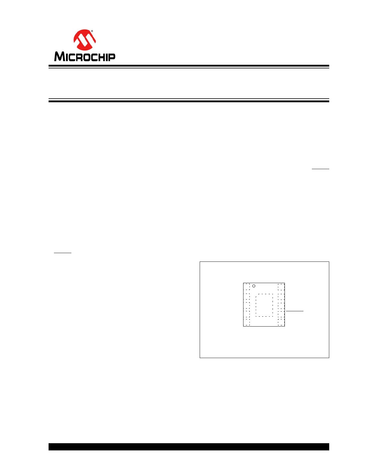
Package Types
SENSE2+
†
SENSE1-
SENSE2-
†
SMCLK
SMDATA
1
2
3
4
10
9
8
7 ALERT
V
DD
SENSE1+
EP
11
6
5
ADDR_SEL
GND
PAC1710/20
3x3 VDFN*
*Includes Exposed Thermal Pad (EP), see
Table 3-1
†PAC1720 only.
Single and Dual High-Side Current-Sense Monitor with
Power Calculation
PAC1710/20
DS20005386B-page 2
2015-2016 Microchip Technology Inc.
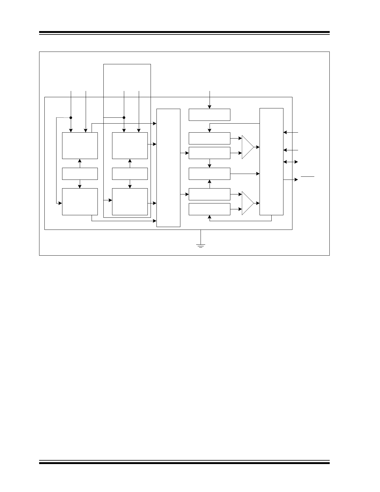
Device Block Diagram
SMBus
Interface
SMCLK
SMDATA
ADDR_SEL
SENSE2+
SENSE2-
Voltage
Registers
Configuration
Current Registers
Current Limits
Voltage Limits
ALERT
Power Register
Current
Measurement
Voltage
Measurement
Power
Management
V
DD
GND
Configuration
Current
Measurement
Voltage
Measurement
SENSE1+
SENSE1-
Analog
MUX
PAC1720 only

2015-2016 Microchip Technology Inc.
DS20005386B-page 3
PAC1710/20
1.0
ELECTRICAL CHARACTERISTICS
1.1
Electrical Specifications
Absolute Maximum Ratings
(†)
V
DD
pin............................................................................................................................................................-0.3 to 6.0V
Voltage on SENSE- and SENSE+ pins.............................................................................................................-42 to 42V
Voltage on any other pin to GND ..................................................................................................-GND-0.3 to V
DD
+0.3V
Voltage between Sense pins (|(SENSE+
–
SENSE-)|)................................................................................................40V
Input current to any pin except V
DD
......................................................................................................................+10 mA
Output short-circuit current.............................................................................................................................. Continuous
Package Power Dissipation (
Note
) ............................................................................................ 0.5W up to T
A
= 85°C/W
Junction to Ambient (
J-A
) .....................................................................................................................................78°C/W
Operating Ambient Temperature Range ......................................................................................................... -40 to 85°C
Storage Temperature Range......................................................................................................................... -55 to 150°C
ESD Rating
–
SMCLK, SMDATA, and ALERT pins
–
HBM.....................................................................................8000V
SD Rating
–
all other pins
–
HBM............................................................................................................................2000V
† Notice
: Stresses above those listed under “Absolute Maximum Ratings” may cause permanent damage to the device.
This is a stress rating only and functional operation of the device at those or any other conditions above those indicated
in the operation listings of this specification is not implied. Exposure above maximum rating conditions for extended peri-
ods may affect device reliability.
Note:
The Package Power Dissipation specification assumes a recommended thermal via design consisting of a
2 x 3 matrix of 0.3 mm (12 mil) vias at 0.9 mm pitch connected to the ground plane with a 1.6 mm x 2.3 mm
thermal landing.
PAC1710/20
DS20005386B-page 4
2015-2016 Microchip Technology Inc.
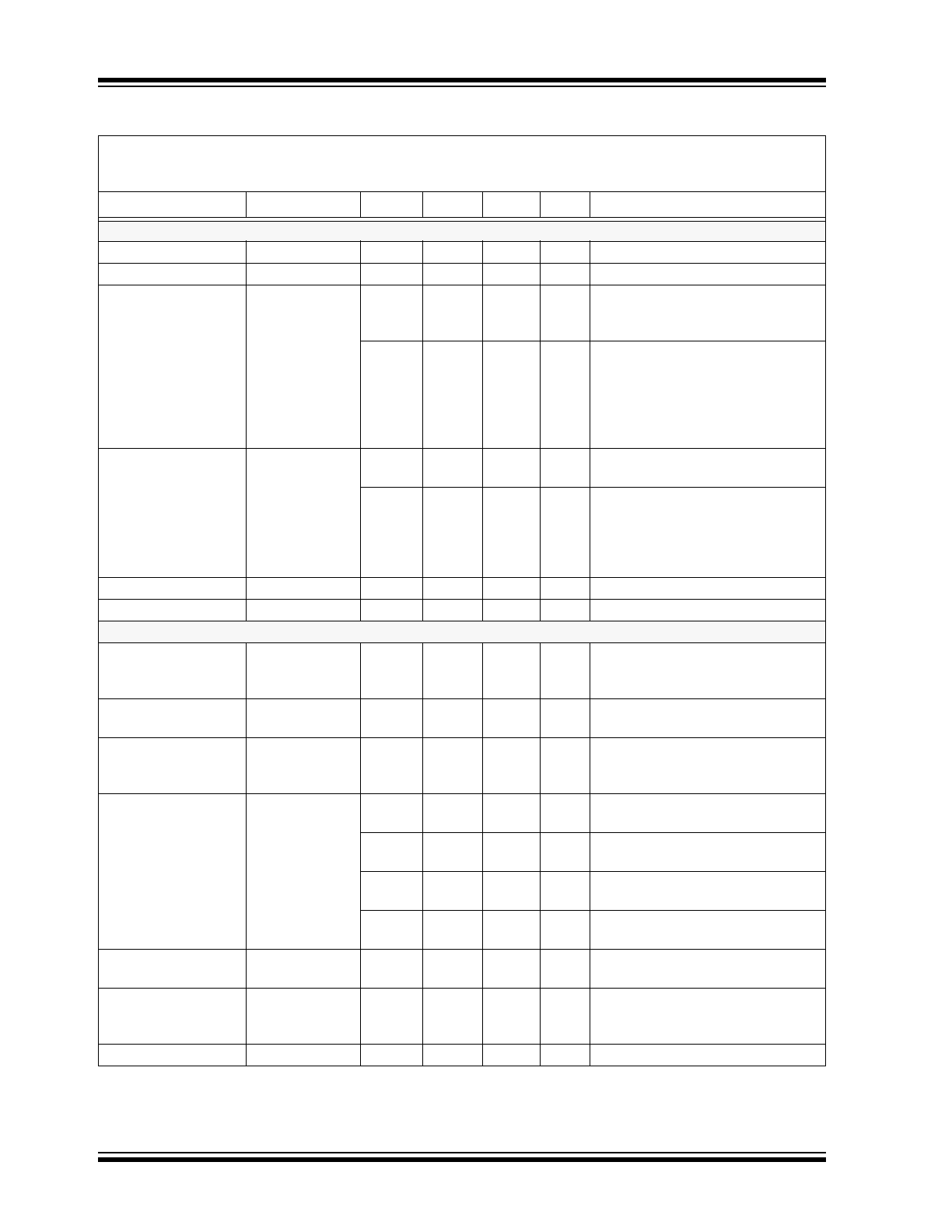
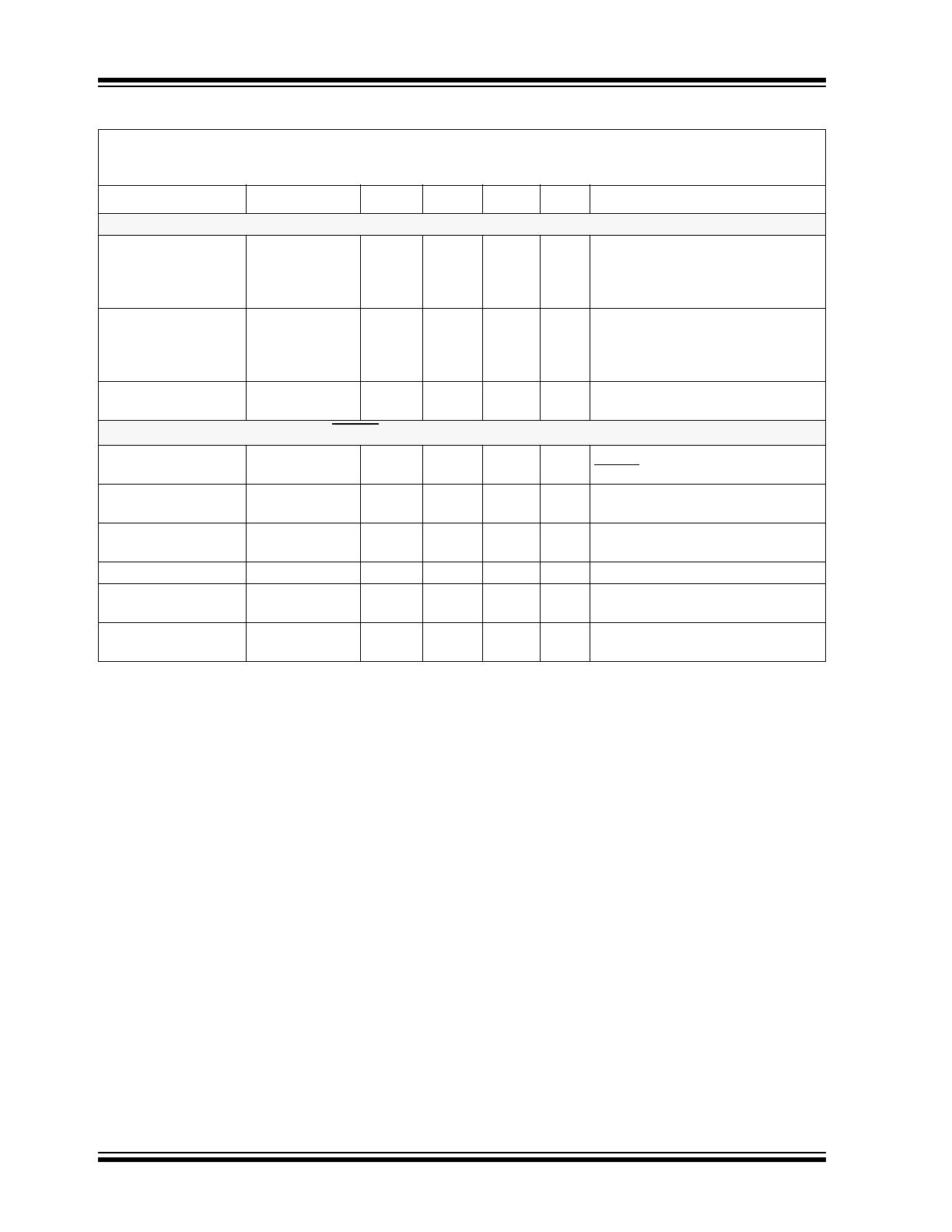
TABLE 1-1:
DC CHARACTERISTICS
Electrical Characteristics
: Unless otherwise specified, maximum values are at T
A
= -40°C to +85°C,
V
DD
= 3V to 5.5V, V
SOURCE
= 0V to 40V; typical values are at T
A
= +25°C, V
DD
= 3.3V, V
SOURCE
= 24V,
V
SENSE
= (SENSE+
–
SENSE-) = 0V; Current Sense Full Scale Range = 80 mV unless otherwise noted
Characteristic
Symbol
Min.
Typ.
Max.
Unit
Conditions
Power Supply
Voltage on SENSE+
V
SOURCE
0
—
40
V
V
DD
Range
V
DD
3.0
—
5.5
V
V
DD
Pin Supply
Current (PAC1720)
I
DD
—
0.525
1.3
mA
Both measurement channels
enabled. Continuous conversions
(see
Table 4-1
)
—
13
50
µA
Both measurement channels
enabled. One conversion per
second (see
Table 4-1
).
VSRC_SAMP_TIME = 2.5 ms
CS_SAMP_TIME = 2.5 ms
No SMBus communications
V
DD
Pin Supply
Current (PAC1710)
I
DD
—
360
900
µA
Continuous Conversions
(see
Table 4-1
)
—
10
35
µA
One conversion per second
(see
Table 4-1
).
VSRC_SAMP_TIME = 2.5 ms
CS_SAMP_TIME = 2.5 ms
No SMBus communications
V
DD
Rise Rate
V
DD_RISE
0.03
V/ms 0 to 3V in 100 ms
V
DD
Standby Current
I
DD_STBY
—
5.5
15
µA
Standby state
Analog Input Characteristics
SENSE+/SENSE-
Pins Common-Mode
Voltage Range
V
CM
0
—
40
V
Common-mode voltage on SENSE
pins, referenced to ground
V
SENSE
Differential
Input Voltage Range
V
DIFF
-80
—
+80
mV
Voltage between SENSE+ and
SENSE- pins
Current-Sense Power
Supply Rejection
Ratio
PSRR_CS
—
10
—
µV/V 3.0V < V
DD
< 5.5V
Full-Scale Range (±)
(see
Section 4.4
“Current
Measurement”
)
FSR
-10
—
10
mV
1 LSB = 4.885 µV
11-bit data resolution
-20
—
20
mV
1 LSB = 9.77 µV
11-bit data resolution
-40
—
40
mV
1 LSB = 19.54 µV
11-bit data resolution
-80
—
80
mV
1 LSB = 39.08 µV
11-bit data resolution
Common-Mode
Rejection
V
SENSE _CMRR
80
100
—
dB
Common-Mode Rejection,
0V < V
SOURCE
< 40V
SENSE+/SENSE-
Pins Common-Mode
Voltage Range
V
CM
0
—
40
V
Common-mode voltage on SENSE
pins, referenced to ground
V
BUS
Gain Accuracy
V
BUS_GAIN_ERR
—
—
±0.4
%
Measured at ADC output, Gain = 1
2015-2016 Microchip Technology Inc.
DS20005386B-page 5
PAC1710/20
SENSE+, SENSE- Pin
Leakage Current
I
SENSE +,
I
SENSE-
—
—
1.0
µA
V
BUS
= 24V, V
SENSE
= 0V
Sleep state
SENSE+, SENSE- Pin
Leakage Current
I
SENSE +,
I
SENSE-
—
—
1.0
µA
V
DD
= 0V
SENSE+ Pin Bias
Current
I
SENSE +
—
100
150
µA
-80 mV < V
SENSE
< 80 mV
Active state
SENSE- Pin Bias
Current
I
SENSE-
—
0.1
1
µA
-80 mV < V
SENSE
< 80 mV
Active state
Current-Sense Offset Error Voltage
Offset Error Voltage
(referred to input)
V
OS
—
±15
—
µV
FSR = ±10 mV
—
±15
—
µV
FSR = ±20 mV
—
±20
—
µV
FSR = ±40 mV
—
±40
—
µV
FSR = ±80 mV
Current-Sense Total Measurement Error
Total Error
(positive range)
(see
Section 4.4
“Current
Measurement”
)
V
SENSE _TOT_ERR
—
±0.5
±1
%
FSR
FSR = 0 to +10 mV
—
±0.3
±0.6
%
FSR
FSR = 0 to +20 mV
—
±0.2
±0.4
%
FSR
FSR = 0 to +40 mV
—
±0.2
±0.4
%
FSR
FSR = 0 to +80 mV
Total Error
(negative range)
(see
Section 4.4
“Current
Measurement”
)
V
SENSE _TOT_ERR
-1
-1.3
-1.6
%
FSR
FSR = -10 mV to 0
-1
-1.3
-1.6
%
FSR
FSR = -20 mV to 0
-1
-1.3
-1.6
%
FSR
FSR = -40 mV to 0
-1.6
-2
-2.4
%
FSR
FSR = -80 mV to 0
V
SOURCE
Voltage Measurement
Power Supply
Rejection Ratio
PSRR
—
10
—
mV/V 3.0V < V
DD
< 5.5V
V
SOURCE
Error (±)
V
SOURCE_ ERR
—
0.15
0.3
%
FSV
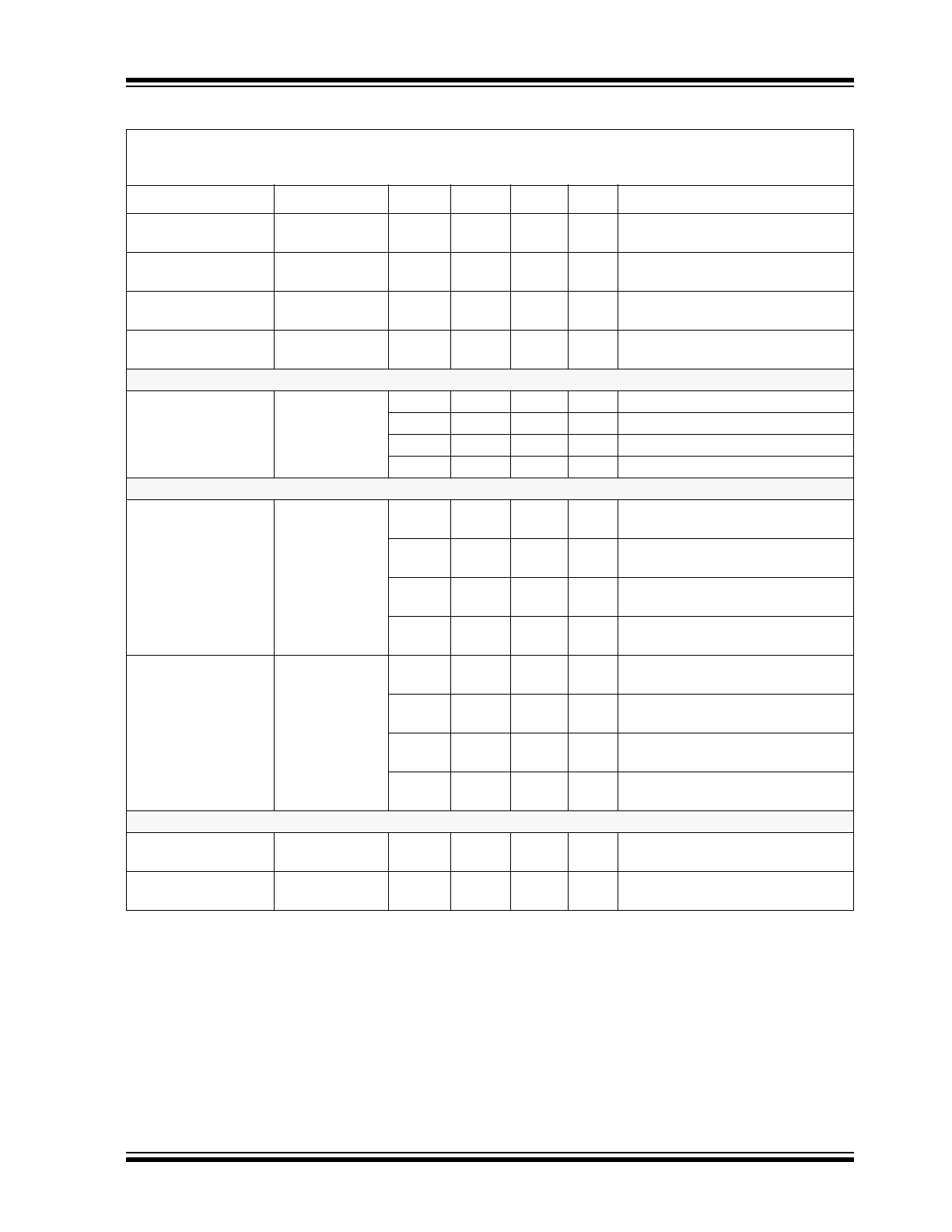
TABLE 1-1:
DC CHARACTERISTICS (CONTINUED)
Electrical Characteristics
: Unless otherwise specified, maximum values are at T
A
= -40°C to +85°C,
V
DD
= 3V to 5.5V, V
SOURCE
= 0V to 40V; typical values are at T
A
= +25°C, V
DD
= 3.3V, V
SOURCE
= 24V,
V
SENSE
= (SENSE+
–
SENSE-) = 0V; Current Sense Full Scale Range = 80 mV unless otherwise noted
Characteristic
Symbol
Min.
Typ.
Max.
Unit
Conditions
PAC1710/20
DS20005386B-page 6
2015-2016 Microchip Technology Inc.
Power Ratio
Total Power Ratio
Measurement Error
(±)
(positive range)
P
RATIO _ERR
—
—
1
%
FSR
FSR = 0 to +10 mV, 0 to +20 mV,
0 to +40 mV, or 0 to +80 mV
Total Power Ratio
Measurement Error
(±)
(negative range)
P
RATIO _ERR
—
—
2
%
FSR
FSR = -10 mV to 0, -20 mV to 0,
-40 mV to 0, or -80 mV to 0
First Power Ratio
Ready
t
CONV_P
—
—
220
ms
Time after power-up before
P
RATIO
updated
Digital I/O Pins (SMCLK, SMDATA, ALERT)
Pull-up Voltage Range
V
PULLUP
3.0
—
5.5
V
Pull-up voltage for SMBus and
ALERT pins
Time to First
Communications
t
COMM
—
—
25
ms
Input High Voltage
V
IH
2.0
—
—
V
SMCLK, SMDATA
OD pins pulled up to V
PULLUP
Input Low Voltage
V
IL
—
—
0.8
V
Output Low Voltage
V
OL
—
—
0.4
V
OD pin pulled to V
PULLUP
3 mA current sink
Leakage Current (±)
I
LEAK
—
—
5
µA
Powered or unpowered
T
A
< +85°C
TABLE 1-1:
DC CHARACTERISTICS (CONTINUED)
Electrical Characteristics
: Unless otherwise specified, maximum values are at T
A
= -40°C to +85°C,
V
DD
= 3V to 5.5V, V
SOURCE
= 0V to 40V; typical values are at T
A
= +25°C, V
DD
= 3.3V, V
SOURCE
= 24V,
V
SENSE
= (SENSE+
–
SENSE-) = 0V; Current Sense Full Scale Range = 80 mV unless otherwise noted
Characteristic
Symbol
Min.
Typ.
Max.
Unit
Conditions
2015-2016 Microchip Technology Inc.
DS20005386B-page 7
PAC1710/20
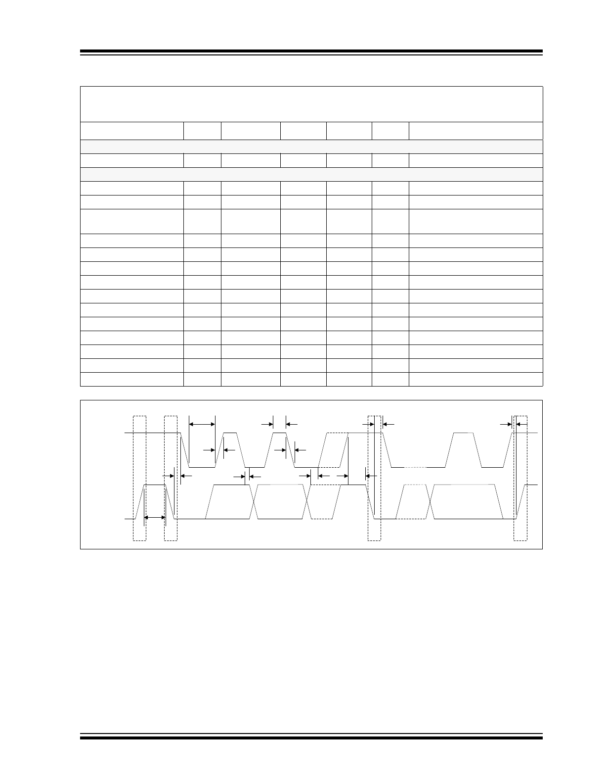
FIGURE 1-1:
SMBus Timing.
TABLE 1-2:
SMBUS MODULE SPECIFICATIONS
Electrical Characteristics
: Unless otherwise specified, maximum values are at T
A
= -40°C to +85°C,
V
DD
= 3V to 5.5V, V
BUS
= 0V to 32V; Typical values are at T
A
= +25°C, V
DD
= 3.3V, V
BUS
= 24V,
V
SENSE
= (SENSE+
–
SENSE-) = 0V
Characteristic
Sym.
Min.
Typ.
Max.
Units
Conditions
SMBus Interface
Input Capacitance
C
IN
—
4
10
pF
SMBus Timing
Clock Frequency
f
SMB
10
—
400
kHz
Spike Suppression
t
SP
—
—
100
ns
Bus Free Time Stop to
Start
t
BUF
1.3
—
—
µs
Start Setup Time
t
SU:STA
0.6
—
—
µs
Start Hold Time
t
HD:STA
0.6
—
—
µs
Stop Setup Time
t
SU:STO
0.6
—
—
µs
Data Hold Time
t
HD:DAT
0
—
—
µs
When transmitting to the master
Data Hold Time
t
HD:DAT
0.3
—
—
µs
When receiving from the master
Data Setup Time
t
SU:DAT
0.6
—
—
µs
Clock Low Period
t
LOW
1.3
—
—
µs
Clock High Period
t
HIGH
0.6
—
—
µs
Clock/Data Fall Time
t
FALL
—
—
300
ns
Min = 20 + 0.1 C
LOAD
ns
Clock/Data Rise Time
t
RISE
—
—
300
ns
Min = 20 + 0.1 C
LOAD
ns
Capacitive Load
C
LOAD
—
—
400
pF
Total per bus line
SMDATA
SMCLK
T
LOW
T
RISE
T
HIGH
T
FALL
T
BUF
T
HD:STA
P
S
S - Start Condition
P - Stop Condition
T
HD:DAT
T
SU:DA
T
T
SU:STA
T
HD:STA
P
T
SU:STO
S

PAC1710/20
DS20005386B-page 8
2015-2016 Microchip Technology Inc.
NOTES:
2015-2016 Microchip Technology Inc.
DS20005386B-page 9
PAC1710/20
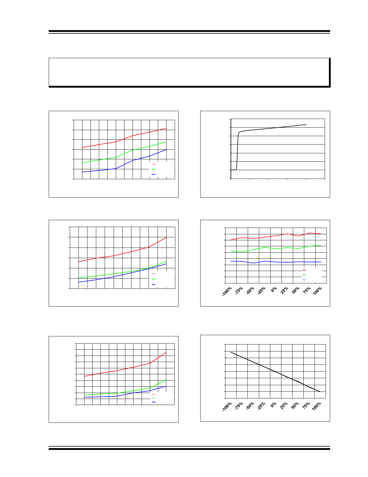
2.0
TYPICAL OPERATING CURVES
Note:
Unless otherwise indicated, maximum values are at T
A
= -40°C to +85°C, V
DD
= 3V to 5.5V, V
SOURCE
= 0V to
40V; typical values are at T
A
= +25°C, V
DD
= 3.3V, V
SOURCE
= 24V, V
SENSE
= (SENSE+
–
SENSE-) = 0V.
FIGURE 2-1:
I
DD
vs. V
DD
, Continuous
Conversions (PAC1710).
FIGURE 2-2:
I
DD
vs. V
DD
, One
Conversion per Second, Lowest Resolution
(PAC1710).
FIGURE 2-3:
I
DD
vs. V
DD
, Standby Mode
(PAC1710)
FIGURE 2-4:
I
SENSE
+ Pin Current vs.
V
BUS
(T
A
=
-40°C to +85°C).
FIGURE 2-5:
I
SENSE
+ Pin Bias Current
(80 mV Range).
FIGURE 2-6:
I
SENSE
- Pin Bias Current
(80 mV Range, T
A
=
-40°C to +85°C).
Note:
The graphs and tables provided following this note are a statistical summary based on a limited number of
samples and are provided for informational purposes only. The performance characteristics listed herein
are not tested or guaranteed. In some graphs or tables, the data presented may be outside the specified
operating range (e.g., outside specified power supply range) and therefore outside the warranted range.
320.0
340.0
360.0
380.0
400.0
420.0
440.0
3.0
3.3
3.6
4.5
5.0
5.5
I
dd
(
μ
A)
V
DD
(V)
T = +85˚C
T = +25˚C
T = -
40˚C
8.0
10.0
12.0
14.0
16.0
18.0
20.0
3.0
3.3
3.6
4.5
5.0
5.5
I
DD
(
μ
A)
V
DD
(V)
T = +85˚C
T = +25˚C
T = -
40˚C
3.000
4.000
5.000
6.000
7.000
8.000
9.000
10.000
11.000
12.000
13.000
3.0
3.3
3.6
4.5
5.0
5.5
I
DD
(
μ
A)
V
DD
(V)
T = +85˚C
T = +25˚C
T = -
40˚C
-20.000
0.000
20.000
40.000
60.000
80.000
100.000
120.000
0
10
20
30
40
50
I
SENSE
+ Current (
μ
A)
V
BUS
(V)
97.5
98.0
98.5
99.0
99.5
100.0
100.5
101.0
101.5
102.0
I
SENSE
+ Current (
μ
A)
V
SENSE
(% of full scale)
T = +85˚C
T = +25˚C
T = -
40˚C
-0.20
-0.15
-0.10
-0.05
0.00
0.05
0.10
0.15
0.20
I
SENSE
- Current
(μ
A)
V
SENSE
(% of full scale)
PAC1710/20
DS20005386B-page 10
2015-2016 Microchip Technology Inc.
FIGURE 2-7:
I
DD
vs. V
DD
, Continuous
Conversions (PAC1720).
FIGURE 2-8:
I
DD
vs. V
DD
, One
Conversion per Second, Lowest Resolution
(PAC1720).
FIGURE 2-9:
I
DD
vs. V
DD
, Standby Mode
(PAC1720).
FIGURE 2-10:
I
SENSE
+ Pin Leakage
Current, T
A
=
-40°C to +85°C.
FIGURE 2-11:
I
SENSE
- Pin Leakage
Current, T
A
=
-40°C to +85°C.
460.0
480.0
500.0
520.0
540.0
560.0
580.0
600.0
3.0
3.3
3.6
4.5
5.0
5.5
I
DD
(
μ
A)
V
DD
(V)
T = +85˚C
T = +25˚C
T = -
40˚C
10.000
12.000
14.000
16.000
18.000
20.000
22.000
3.0
3.3
3.6
4.5
5.0
5.5
I
DD
(
μ
A)
V
DD
(V)
T = +85˚C
T = +25˚C
T = -
40˚C
3.000
4.000
5.000
6.000
7.000
8.000
9.000
10.000
11.000
12.000
13.000
3.0
3.3
3.6
4.5
5.0
5.5
I
DD
(
μ
A)
V
DD
(V)
T = +85˚C
T = +25˚C
T = -
40˚C
-0.020
-0.015
-0.010
-0.005
0.000
0.005
0.010
I
SENSE
+ C
urrent [
μ
A]
V
SENSE
(% of full scale)
-0.020
-0.015
-0.010
-0.005
0.000
0.005
0.010
I
SENSE
+ C
urrent (
μ
A)
V
SENSE
(% of full scale)