

2016 Microchip Technology Inc.
DS20005640A-page
1
HV98100/HV98101
Features
• Good LED Current Regulation
- Better than 5% accuracy
• Valley Switching Buck-Boost Converter with
Power Factor Correction (PFC)
- 0.97 Power Factor (typical)
- 5% Total Harmonic Distortion (THD) (typical)
• Uses a Standard Off-the-Shelf Inductor
- No auxiliary winding required
• Single Input Voltage Range
- HV98100: 110
V
AC
±15%
- HV98101: 230
V
AC
±15%
• Supports 5W-15W Output Power
• Space-saving SOT-23-6L Package
Applications
• LED Lamps
• LED Lighting Fixtures
Description
The HV98100/HV98101 LED driver integrated circuit
(IC) is an off-line, high-power factor, buck-boost
controller targeted at general LED lighting products,
such as LED lamps and LED lighting fixtures with a
maximum power rating of about 15W.
Valley-switching buck-boost converters are preferred in
off-line applications since they reduce switching losses.
A typical solution is to pair a constant on-time control
scheme with valley switching to achieve both a
high-power factor and good efficiency. However, this
control scheme results in a higher total harmonic distor-
tion, and the actual value is dependent on the input and
output voltages. The HV98100/HV98101 uses a unique
control scheme to achieve a high-power factor and low
THD simultaneously under all line and load conditions,
while maximizing efficiency utilizing valley switching.
The average LED current is also controlled in a closed-
loop manner to achieve high LED accuracy.
Other unique features of the ICs are the bootstrap of
the IC supply voltage from the output, as well as the
unique valley-sensing scheme that allows the use of a
standard off-the-shelf inductor to minimize the overall
system cost.
Applications with low-output voltage can be
accommodated using a coupled inductor.
Package Types
4
1
2
3
6 GATE
CS
IND
GND
COMP
5 PV
DD
HV98100/HV98101
6-Lead SOT-23
See
Table
3-1
for pin description.
Non-Dimmable, Off-Line, LED Driver with Low Total
Harmonic Distortions
HV98100/HV98101
DS20005640A-page
2
2016 Microchip Technology Inc.
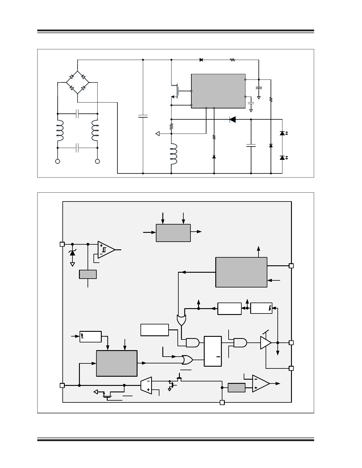
Typical Application Circuit
HV98100/1
GT
GN
D
CS
IN
D
COMP
P
VDD
M
BBT
L
BBT
R
CS
D
BBT
LED
C
COMP
C
REC
D
PVDD
R
PVDD
C
O
C
PVDD
R
HV
D
HV
R
VD
D
VD
V
AC
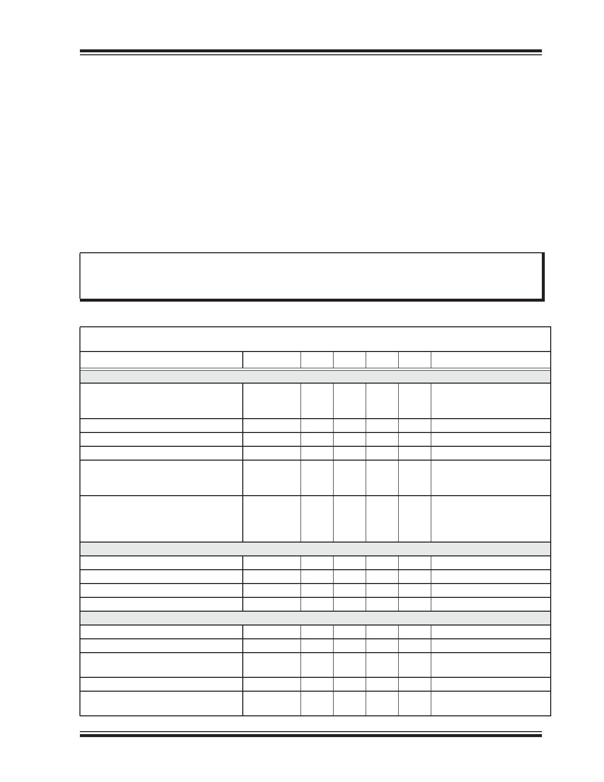
Internal Block Diagram
Monos hot
COMP
S
R
Q
Q
GATE
P
VDD
P
VDD
Startup
clock
V
al
ley
_
D
et
GT_ON
Gate
VDD
on
/VDD
of f
THD
control
POR
GND
P
VDD
IND
Valley Detect
RE
F
GT
_
R
RES E T
Monos hot
Gate
RE
S
E
T
Gate
IN
DE
T
_
V
A
L
GATE
I_V O
f
sta rt
POR
FLT
I_VO
CS
CS_REF
Fault
Pr otection
I_VO
FLT
Gate
Reg
ST RT_UP
Vton_ref
V_TON
POR
Max F req
Clock
A
VDD
Gate
Gate
LEB
OCP_REF
OCP
OCP
2016 Microchip Technology Inc.
DS20005640A-page
3
HV98100/HV98101
1.0
ELECTRICAL CHARACTERISTICS
Absolute Maximum Ratings†
Supply Voltage PV
DD
to GND .....................................................................................................................-0.3V to +20V
GATE
to GND.................................................................................................................................-0.3V to (PV
DD
+0.5V)
CS, COMP, IND
to GND............................................................................................................................... -0.3V to 4.5V
Operating Junction Temperature.............................................................................................................-40°C to +125°C
Storage Temperature ..............................................................................................................................-65°C to +150°C
Power Dissipation at +25°C for 6L-SOT-23 .........................................................................................................800
mW
ESD Protection on all pins (HBM) ..............................................................................................................................2
kV
ESD Protection on all pins (MM) ...............................................................................................................................175V
* Based on JEDEC JESD51 testing and reporting standards
†
Notice:
Stresses above those listed under “Maximum Ratings” may cause permanent damage to the device. This is
a stress rating only and functional operation of the device at those or any other conditions above those indicated in
the operational sections of this specification is not intended. Exposure to maximum rating conditions for extended
periods may affect device reliability.
ELECTRICAL CHARACTERISTICS
Electrical Specifications
: Unless otherwise specified, all specifications are for T
A
=
T
J
=
+25°C, PV
DD
=
12V. Boldface
specifications apply over the full temperature range T
A
=
T
J
=
-40°C to +125°C.
Parameter
Symbol
Min.
Typ.
Max.
Units
Conditions
Power Supply (PV
DD
)
PV
DD
Clamp Voltage
PV
DD,clamp
15.5
17
18.5
V
Current into PV
DD
= 4.0
mA;
C
GATE
=
500
pF;
f
sw
=
100
kHz;
V
DD
Start Voltage
V
DD,ON
14.5
16
17.5
V
GATE starts switching
V
DD
Stop Voltage
V
DD,OFF
6.5
8
9.5
V
GATE stops switching
Current into clamp
I
DD,max
—
—
5
mA
Note
1
Current drawn by IC before start
I
DD,Q
—
—
200
μA
Measured at PV
DD
=
12V
after PV
DD
rises from 0V to
12V
Current drawn by IC during operation
I
DD,OP
—
—
4.3
mA
C
GATE
=
500
pF;
f
sw
=
100
kHz; COMP
=
3V;
I_IND
SINK
=
200
μA;
I_IND
SOURCE
=
250
μA
Gate Driver
GATE Driver Sourcing Current
I
SOURCE
0.3
—
—
A
Note
2
Gate Driver Sinking Current
I
SINK
0.6
—
—
A
Note
2
Gate Rise Time (10%-90%)
T
RISE
—
—
45
ns
C
GATE
=
500
pF
Gate Fall Time (10%-90%)
T
FALL
—
—
23
ns
C
GATE
=
500
pF
Output Current Control
Internal Reference Voltage
CS
REF
194
204
214
mV
Note
2
OTA Offset Voltage
V
OFFSET
-7.5
—
7.5
mV
Note
2
Open Loop DC Gain
A
V
55
—
—
dB
1V
COMP
4V; Output
open
Note
1
Small Signal Transconductance
g
m
160
230
300
μA/V 1V
COMP 4V;
Note
1
Gain Bandwidth Product
GBW
0.16
0.24
—
MHz
CCOMP = 150
pF
(
Note
2
)
HV98100/HV98101
DS20005640A-page
4
2016 Microchip Technology Inc.
R
ON
of COMP Reset FET
R
COMP
300
400
500
Internal Clocks
Start-up Clock
F
start
6.25
10
15
kHz
Maximum Frequency Limit
F
max
217
320
480
kHz
Note
1
Valley Detect
Current into IND pin
I
IND
—
—
600
μA
Note
2
Voltage at IND pin
V
IND
3.87
4.3
4.73
V
I
IND
=
250
μA
Comparator Delay Time
T
delay
—
—
50
ns
Note
2
Control Circuit
Internal Timing Constant
K
T
—
1.25
—
μs
Internal Voltage for Timing
V
Tref
—
2
—
V
HV98100
—
2.5
—
V
HV98101
GATE On-time
T
ON
6.83
7.35
7.89
μs
HV98100
Ext Clk = 50
kHz
COMP = 2V
T
ON
6.11
6.7
7.05
μs
HV98101
Ext CSlk = 50
kHz
COMP = 2V
Protection
Over Voltage Protection Current
Threshold
I
OVP
350
450
550
μA
GATE
=
LOW
Over Current Protection Reference
OCP
REF
2.2
2.35
2.5
V
Over Current Protection Blanking Time
T
BLNKOCP
150
—
250
ns
Note
2
Detect time for Over Current Protection
T
DETOCP
150
—
250
ns
After TBLNKOCP (
Note
2
)
Over Current Comparator Delay
OCP
DLY
—
50
100
ns
100
mV overdrive (
Note
2
)
Note 1:
Obtained by Design and Characterization; not 100% tested in production.
2:
Design Guidance only.
TABLE 1-1:
TEMPERATURE SPECIFICATIONS
Parameter
Symbol
Min.
Typ.
Max.
Units
Conditions
Temperature Ranges
Storage Temperature
T
A
-65
—
+150
°C
Operating Junction Temperature
T
J
-40
—
+125
°C
Thermal Package Resistance
Thermal Resistance, 6L-SOT-23
JA
—
124
—
°C/W
JC
—
74
—
°C/W
ELECTRICAL CHARACTERISTICS (CONTINUED)
Electrical Specifications
: Unless otherwise specified, all specifications are for T
A
=
T
J
=
+25°C,
PV
DD
=
12V.
Boldface
specifications apply over the full temperature range T
A
=
T
J
=
-40°C to +125°C.
Parameter
Symbol
Min.
Typ.
Max.
Units
Conditions
2016 Microchip Technology Inc.
DS20005640A-page
5
HV98100/HV98101
2.0
TYPICAL OPERATING CURVES
Note:
The graphs and tables provided following this note are a statistical summary based on a limited number of
samples and are provided for informational purposes only. The performance characteristics listed herein
are not tested or guaranteed. In some graphs or tables, the data presented may be outside the specified
operating range (e.g., outside specified power supply range) and therefore outside the warranted range.
Note:
Unless otherwise indicated, T
A
=
T
J
=
+25°C, PV
DD
=
12V. Boldface specifications apply over the full temperature
range T
A
=
T
J
=
-40°C to +125°C.
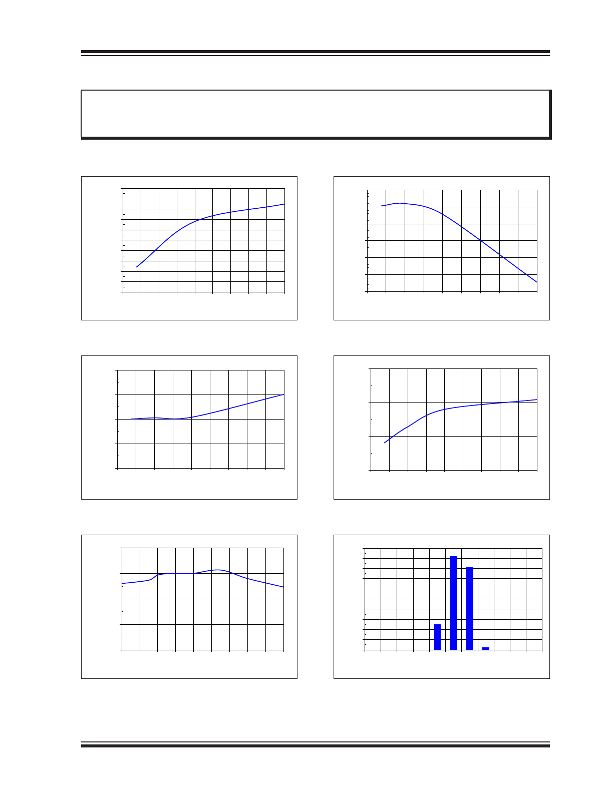
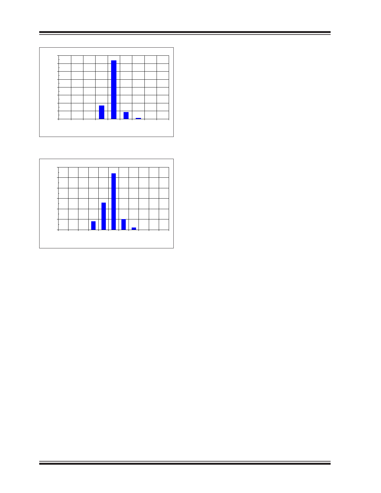
15.6
15.65
15.7
15.75
15.8
15.85
15.9
15.95
16
16.05
16.1
-55 -35 -15
5
25
45
65
85 105 125
V
DD,ON
(V)
Temperature (°C)
FIGURE 2-1:
V
DD
Start Voltage vs.
Junction Temperature.
7.9
7.95
8
8.05
8.1
-55 -35 -15
5
25
45
65
85
105 125
V
DD,ON
(V)
Temperature (°C)
FIGURE 2-2:
V
DD
Stop Voltage vs.
Junction Temperature.
199
199.5
200
200.5
201
-55 -35 -15
5
25
45
65
85 105 125
CS
REF
(mV)
Temperature (°C)
FIGURE 2-3:
Internal Reference Voltage
vs. Junction Temperature.
430
435
440
445
450
455
460
-55 -35 -15
5
25
45
65
85
105 125
I
OVP
(uA)
Temperature (°C)
FIGURE 2-4:
Over Voltage Protection
Current Threshold vs. Junction Temperature.
2.37
2.38
2.39
2.4
-55 -35 -15
5
25
45
65
85 105 125
OCP
REF
(V)
Temperature (°C)
FIGURE 2-5:
Over Current Protection
Reference vs. Junction Temperature.
0
5
10
15
20
25
30
35
40
45
50
7
7.5
8
8.5
9
9.5 10 10.5 11 11.5 12
%
of
Units
F
START
(kHz)
FIGURE 2-6:
Startup Clock Frequency
Histogram.
0
10
20
30
40
50
60
70
80
125 135 145 155 165 175 185 195 205
%
of
Units
I
DD,Q
(uA)
HV98100/HV98101
DS20005640A-page
6
2016 Microchip Technology Inc.
FIGURE 2-7:
Quiescent Current
Histogram.
0
10
20
30
40
50
60
90 92 94 96 98 100 102 104 106 108 110
%
of
Units
Output Current (mA)
FIGURE 2-8:
Output Current Accuracy in
Application.
2016 Microchip Technology Inc.
DS20005640A-page
7
HV98100/HV98101
3.0
PIN DESCRIPTION
The description of the pins are listed in
Table
3-1
.
TABLE 3-1:
PIN DESCRIPTION
HV98100/HV98101
SOT-23
Symbol
Description
1
IND
Input from LED String Anode for both valley detection and over-voltage protection
Pin
2
GND
Common connection for all circuits Pin
3
COMP
Loop compensation for stable response Pin
4
CS
Current sense input for sensing inductor current Pin
5
PV
DD
Supply Voltage for the IC Pin
6
GATE
Gate driver for driving the external MOSFET Pin
3.1
IND
This pin is used for detecting the valley, as well as for
over-voltage protection. The voltage at pin is main-
tained at approximately 4.3V.
When the switching FET
is off, current is sourced out of this pin. If this current
exceeds 450
μA, then
over voltage is detected and the
IC shuts down. This current sourced out of the pin is
also used to detect the valley, using a patented method.
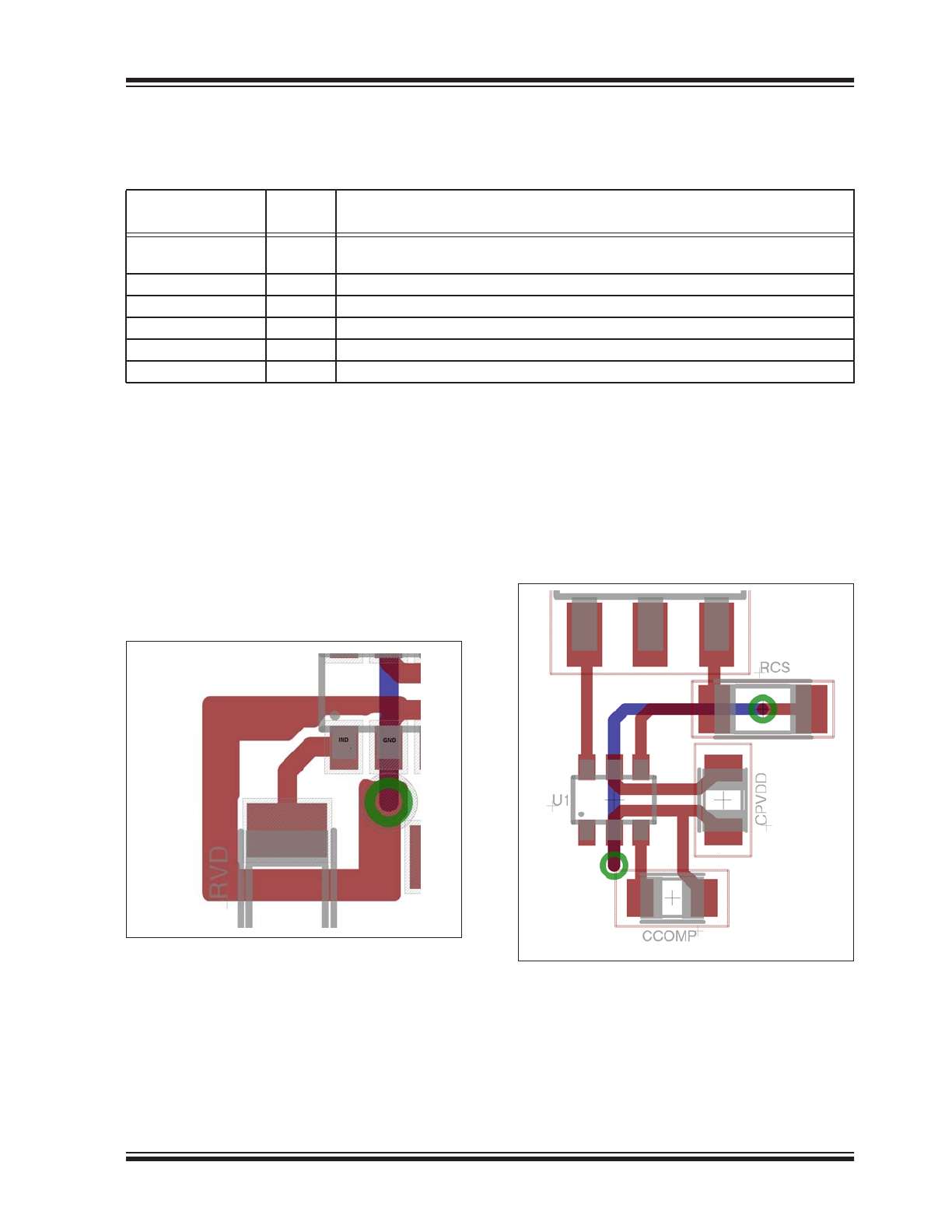
For proper operation, the IND pin should be shielded to
prevent mis-triggering due to the large voltage slew
rates present in application. A recommended layout is
shown in
Figure
3-1
.
FIGURE 3-1:
Shielding the IND Pin.
3.2
Power Ground Pin (GND)
This is the ground pin of the IC. The V
DD
capacitor and
COMP network should be connected to this pin and the
GND pin should be connected to the sense resistor, as
shown in the
Typical Application Circuit
for proper
functioning of the IC.
Figure
3-2
shows a
recommended layout. Red traces in the layout are on
the top layer, whereas blue traces on the layout are on
the bottom layer.
FIGURE 3-2:
Connection to the GND Pin.

HV98100/HV98101
DS20005640A-page
8
2016 Microchip Technology Inc.
3.3
COMP
This pin is the output of the internal transconductance
amplifier. A compensation network connected between
COMP and GND pins is used to stabilize the closed
loop control of the LED current.
3.4
CS
This pin is used to sense the inductor current. The
inductor current information is used to derive the output
LED current, as well as to protect the inductor from
saturation.
3.5
PV
DD
This pin is the power supply pin for the IC. A minimum
of 4.7
μF capacitor needs to be connected between
PV
DD
and GND for stability of the internal shunt regu-
lator. The C
PVDD
capacitor needs to be placed physi-
cally close to the IC to minimize the trace length
between the PV
DD
pin and the capacitor.
3.6
GATE
This pin is the gate drive output of the IC and is used to
control the switching of the external FET.

2016 Microchip Technology Inc.
DS20005640A-page
9
HV98100/HV98101
4.0
FUNCTIONAL DESCRIPTION
4.1
Introduction
The HV98100/HV98101 control ICs provide constant
average LED current for LED lamps and fixtures with a
single-stage, valley-switching, buck-boost power-
supply topology.
The IC is targeted at designs at a single-line voltage,
such as 110
V
AC
(HV98100) or 230
V
AC
(HV98101)
and does not support designs for universal input volt-
age range.
4.2
Principle of Operation
The IC adopts a novel control mechanism to vary both
on-time and switching period at the same instant over
the line cycle in a way that forces the average input cur-
rent to be proportional to the input voltage, realizing
high-power factor and low THD which is independent of
the load voltage (V
O
) (unlike a constant on-time control
where the THD is dependent on the LED string volt-
age).
In order to determine the LED current regulation, power
balancing is used to maintain the mean programmable
LED current (I
O
) in a closed-loop manner by means of
the adaptive V
COMP
swing upon the defined input/out-
put voltage variation, as shown in
Equation
4-1
.
EQUATION 4-1:
I
O
V
2
in,rms
K
T
V
COMP
V
O
---------------------------------------------------------------
=
Assume a V
COMP
variation from 1.2V to 3.8V, an input
voltage (V
IN,rms
) variation of ±15% and the internal tim-
ing constant (K
T
) variation of ±12%. With these
assumptions, the maximum variation in the LED string
voltage (to maintain constant LED current) cannot
exceed ±18% approximately.
HV98100/HV98101
DS20005640A-page
10
2016 Microchip Technology Inc.
5.0
APPLICATION INFORMATION
5.1
Introduction
This section describes the operation of the various
blocks in the IC. Detailed design information, along with
a design example, is provided in
Section
6.0 “Design
Example”
.
5.2
PV
DD
Regulator
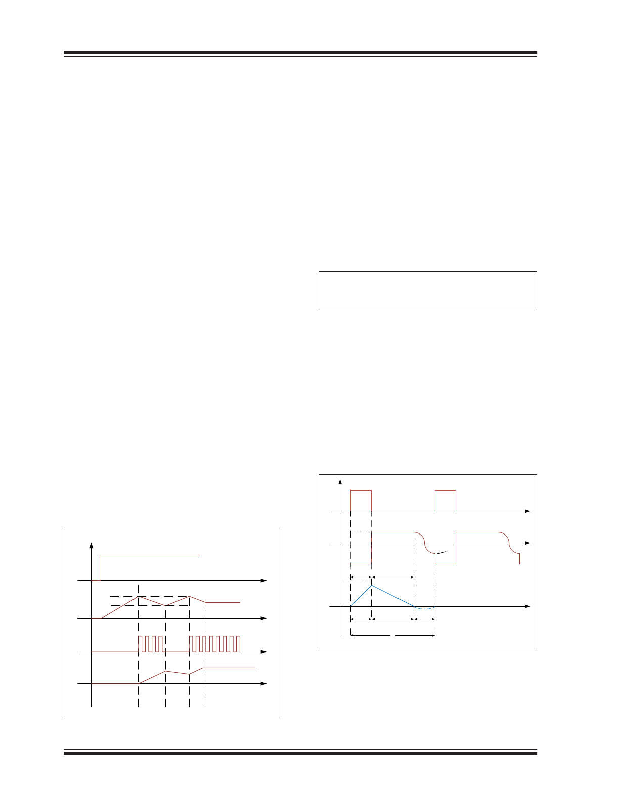
The supply current is initially fed from the rectified AC
input directly via an external start-up resistor (R
HV
) to
peak charge a hold-up capacitor (C
PVDD
) connected at
this pin. Note that a switching diode (D
HV
) is required in
series to prevent the capacitor from discharging when
the buck-boost converter FET (M
BBT
) turns on. As the
voltage on the V
DD
capacitor increases, the IC is held
in a Stand-by mode and draws minimum current
(200
μA max.). Once the voltage at V
DD
reaches
V
DD,ON
, the IC turns on and starts switching at an inter-
nally fixed switching frequency of 10
kHz, until the val-
ley can be detected. Once the valley is detected, the
converter starts working in the normal Valley-Switching
mode
and tries to regulate the LED current. In this
mode, the current drawn by the IC from V
DD
increases
causing the voltage across the V
DD
capacitor to start
dropping (since the current supplied by the external
start-up resistor is not sufficient).
If the V
DD
voltage drops below V
DD,OFF
, the IC enters
into Stand-by mode and the process starts again. If the
bootstrap from the output capacitor (C
O
) is available to
prevent the V
DD
voltage from going below V
DD,OFF
,
then the LED driver operates normally. In this way, as
shown in
Figure
5-1
, the PV
DD
voltage bounces
between V
DD,ON
and V
DD,OFF
within a hysteresis band
for the IC to start GATE switching, until the energy
stored in the output capacitor can be partially delivered
to PV
DD
through the bootstrapping resistor-diode net-
work (R
PVDD
-D
PVDD
).
V
DDON
V
IN
P
VDD
0
0
GT
V
DDOF F
0
V
O
0
FIGURE 5-1:
Typical Startup Waveforms.
The IC includes an internal V
DD
clamp circuit. The
clamp limits the voltage on the V
DD
supply pin to the
maximum value (PV
DD,clamp
). If the maximum current
supplied through the external resistors minus the cur-
rent consumption of the IC is lower than the maximum
value that the Zener clamp can sustain (I
DD,MAX
), no
external Zener diode is required.
5.3
LED Current Regulator
The LED current (I
O
) is sensed directly using an exter-
nal sense resistor R
CS
and compared to an internal
fixed reference (CS
REF
). An internal transconductance
amplifier is used to close the loop on the LED current
with an external compensation capacitor. The LED cur-
rent can be programmed as in
Equation
5-1
.
EQUATION 5-1:
I
LED
CS
REF
R
CS
--------------------
=
5.4
Valley Switching
The driver incorporates valley switching (quasi-reso-
nant switching), a technique for reducing switching loss
at the turn-on event of the buck-boost converter FET.
Valley detect is accomplished by sensing the current
sunk into the IND pin when the GATE is low. The oper-
ation is illustrated in
Figure
5-2
. When the inductor cur-
rent I
L
has decreased to zero at t
2
, the positive LED
voltage V
L
starts to oscillate around the 0V level (with
respect to the IC GND), with an amplitude V
O
. The
GATE turns on again when the first lowest level (valley)
is detected.
+Vo
-V
IN
Gate
V
L
0
0
0
magne tization
I
L
demag netization
valley
t
0
T
on
t
1
t
2
t
00
T
S
3
T
off
I
L,max
FIGURE 5-2:
Valley Detect Waveforms.
However, in case the valley is not detected (during
startup, output short circuit and input voltage zero
crossings), a 10
kHz internal clock is used to start the
next cycle.