
2010-2013 Microchip Technology Inc.
DS22260C-page 1
Features
• 750 mA Continuous Output Current
• Load Voltage Supply: 10V to 40V
• Full Bipolar Stepper Motor Drive Capability
• Bidirectional DC Motor Capability
• Internal Fixed T
OFF
Time PWM Current Control
• Internal Protection Diodes
• Internal Thermal Shutdown
• Under Voltage Lockout
• LS-TTL Compatible Logic Inputs with Pull-Up
Resistors
• Low R
ON
Output Resistance
• Low Quiescent Current
• Operating Temperature Range: -40°C to +105°C
• Pin Compatible with Allegro 6219
Applications
• Stepper Motor Actuators
• DC Motor Actuators
• Automotive HVAC Ventilation
• Automotive Power Seats
Description
The MTS62C19A motor driver is a CMOS device capa-
ble of driving both windings of a bipolar stepper motor
or bidirectionally control two DC motors. Each of the
two independent H-bridge outputs is capable of sus-
taining 40V and delivering up to 750 mA of continuous
current. The output current level is controlled by an
internal pulse-width modulation (PWM) circuit that is
configured using two logic inputs, a current sense
resistor, and a selectable reference voltage. The
H-bridge outputs have been optimized to provide a low
output saturation voltage drop.
Full, half and micro-stepping operations are possible
with the PWM current control and logic inputs. The
maximum output current is set by a sensing resistor
and a user-selectable reference voltage. The output
current limit is selected using two logic level inputs. The
selectable output current limits are 0%, 33%, 67% or
100% of the maximum output current. Each bridge has
a PHASE input signal which is used to control the
direction of current flow through the H-bridge and the
load.
The H-bridge power stage is controlled by non-overlap-
ping signals which prevent current cross conduction
when switching the direction of the current flow. Internal
clamp diodes protect against inductive transients.
Thermal protection circuitry disables the outputs when
the junction temperature exceeds the safe operating
limit. No special power-up sequencing is required.
Undervoltage Lockout circuitry prevents the chip from
operating when the load supply is applied prior to the
logic supply.
The device is supplied in a 24-pin SOP Package.
Package Types
Note:
The MTS62C19A device is formerly a
product of Advanced Silicon.
GND
1
2
3
4
24
23
22
21
20
19
18
17
5
6
7
8
I01
V
LOAD
OUT1A
OUT2A
SENSE2
COMPIN2
OUT2B
GND
16
9
V
REF1
I11
PHASE1
GND
GND
I02
SENSE1
15
10
I12
PHASE2
OUT1B
COMPIN1
MTS62C19A
SOP-24
V
REF2
RC2
RC1
V
LOGIC
11
12
14
13
Dual Full-Bridge Motor Driver
MTS62C19A
MTS62C19A
DS22260C-page 2
2010-2013 Microchip Technology Inc.
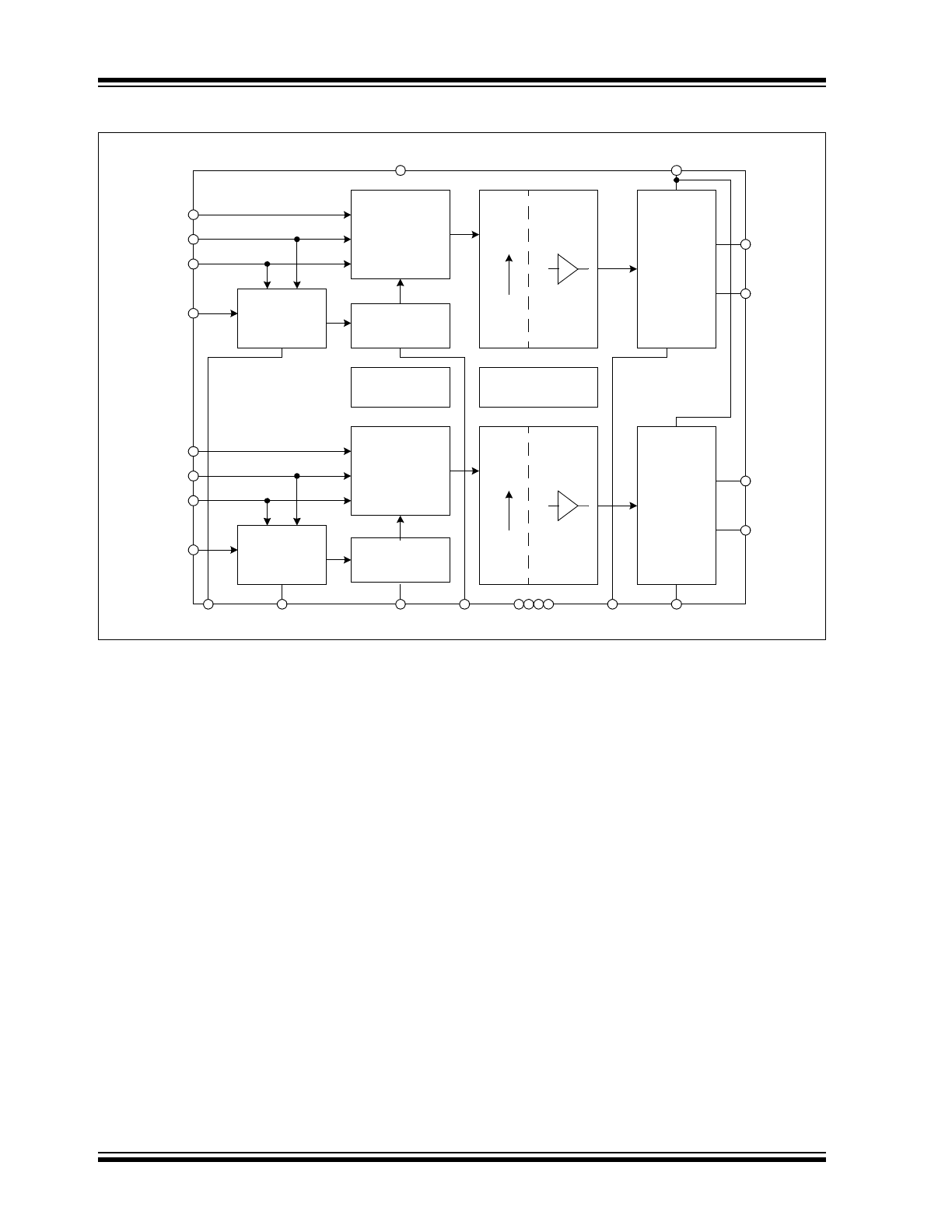
Functional Block Diagram
V
LOGIC
Logic
Shift
Drivers
Power
Bridge
Power
Bridge
Shift
Drivers
Thermal
Shutdown
One-shot
Logic
Current
Sense
Comparator
Current
Sense
Comparator
One-shot
Under-V
Lockout
COMPIN1
COMPIN2
RC2
RC1
GND
SENSE1
SENSE2
OUT2B
OUT2A
OUT1B
OUT1A
V
LOAD
V
REF1
V
REF2
PHASE1
PHASE2
I01
I11
I02
I12
2010-2013 Microchip Technology Inc.
DS22260C-page 3
MTS62C19A
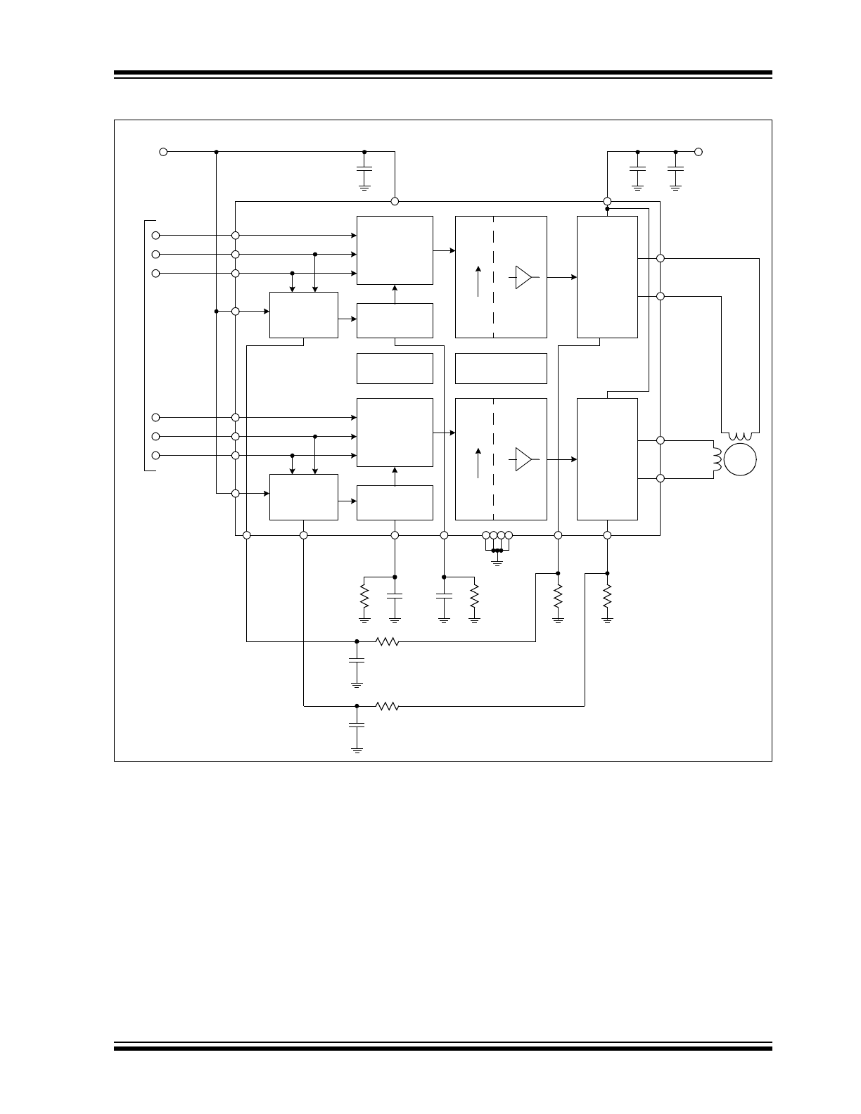
Typical Application
5V
V
LOGIC
V
LOAD
10 to 30V
V
REF1
V
REF2
100 nF
PHASE1
PHASE2
I01
I11
I02
I12
100 nF
100 µF
Logic
Logic
Current
Sense
Comparator
Current
Sense
Comparator
M
One-shot
One-shot
Under-V
Lockout
Thermal
Shutdown
Shift
Drivers
Shift
Drivers
OUT1A
OUT1B
OUT2A
OUT2B
COMPIN1
COMPIN2
RC2
RC1
GND
SENSE1
SENSE2
R
S
R
S
C
t
R
t
R
t
R
C
R
C
C
t
C
C
C
C
Logic/
µP
Power
Bridge
Power
Bridge

MTS62C19A
DS22260C-page 4
2010-2013 Microchip Technology Inc.
1.0
ELECTRICAL
CHARACTERISTICS
Absolute Maximum Ratings †
Logic Supply Voltage (V
LOGIC
)
......................... -0.3 to +5.5V
Load Supply Voltage (V
LOAD
) .......................... -0.3 to +40.0V
Logic Input Voltage Range (V
IN
) ....... -0.3 to VLOGIC + 0.3V
V
REF
Voltage Range (V
REF
) ............................. -0.3 to +10.0V
Output Current (Peak) ..................................................... ±1A
Output Current (Continuous) ...................................... ±0.75A
Sense Output Voltage ...................................... -0.3V to 1.5V
Junction Temperature (T
J
).............................-40°C to +150°C
Operating Temperature Range (T
OPR
)..........-40°C to +105°C
Storage Temperature Range (T
STG
) .............-55°C to +150°C
† Notice: Stresses above those listed under “Maximum
Ratings” may cause permanent damage to the device.
This is a stress rating only and functional operation of
the device at those or any other conditions above those
indicated in the operational listings of this specification
is not implied. Exposure to maximum rating conditions
for extended periods may affect device reliability.
ELECTRICAL CHARACTERISTICS
Electrical Specifications: Unless otherwise specified, all limits are established for V
LOGIC
= 4.5V to 5.5V,
V
LOAD
= 30V,V
REF
= 5V, T
A
= +25°C
Parameters
Sym
Min
Typ
Max
Units
Conditions
DC Characteristics
Logic Supply Voltage
V
LOGIC
4.5
5.0
5.5
V
Load Supply Voltage
V
LOAD
10
30
40
V
Logic Supply Current
I
VLOGIC
—
0.8
1.0
mA
V
REF
Voltage Range
V
REF
1.5
5.0
7.0
V
Driver Supply Current
I
VLOAD_ON
—
0.55
1.0
mA
Both Bridges ON, No Load
I
VLOAD_OFF
—
0.55
1.0
mA
Both Bridges Off
Control Logic
Input Current (V
IN
= 0V)
I
IN
—
—
-70
µA
I01, I11, I02, I12, PHASE1,
PHASE2, (
Note 1
)
Logic-Low
Input Voltage
V
IL
—
—
0.8
V
I01, I11, I02, I12, PHASE1,
PHASE2
Logic-High
Input Voltage
V
IH
2.4
—
—
V
I01, I11, I02, I12, PHASE1,
PHASE2
Current Limit Threshold
Ratio (V
REF
÷ V
SENSE
)
V
REF
_V
SENSE
9.5
10
10.5
—
I0 = L, I1 = L
13.5
15
16.5
—
I0 = H, I1 = L
25.5
30
34.5
—
I0 = L, I1 = H
Driver Output Satura-
tion Voltage V
CE(SAT)
V
ONN
(Low Side)
—
0.55
0.65
V
(Sink) I
OUT
= +500 mA
—
0.90
1.00
V
(Sink) I
OUT
= +750 mA
V
ONP
(High Side)
—
1.05
1.40
V
(Source) I
OUT
= -500 mA
—
1.85
2.10
V
(Source) I
OUT
= -750 mA
Clamp Diode Forward
Voltage (
Note 2
)
V
F_NDIODE
—
0.95
1.30
V
I
F
= 750 mA
V
F_PDIODE
—
1.00
1.30
V
I
F
= 750 mA
Driver Output
Leakage Current
I
LEAK
—
—
-50
µA
V
OUT
= 0V
—
—
50
µA
V
OUT
= V
LOAD
Thermal Shutdown
Temperature
T
J_SHDN
—
170
—
°C
AC Characteristics
Cut-off Time
(one-shot pulse)
T
OFF
—
50
58
µs
R
s
= 1
, R
C
= 1 k
, C
C
= 820 pF,
R
t
= 56 k
, C
t
= 820 pF
Turn-off Delay
T
D
—
1.5
10
µs
Note
1:
V
IN
= 5.0V input current given by internal pull-up to Logic Supply.
2:
Clamp/Freewheel diode is the intrinsic body-drain diode of the NMOS and PMOS transistors.

2010-2013 Microchip Technology Inc.
DS22260C-page 5
MTS62C19A
TEMPERATURE SPECIFICATIONS
Parameters
Sym
Min
Typ
Max
Units
Conditions
Recommended Temperature Ranges
Junction Temperature Range
T
J
-40
+125
°C
Operating Temperature Range
T
A
-40
+105
°C
Thermal Package Resistance
Thermal Resistance, SOP-24
JA
—
76
—
°C/W
EIA/JEDEC JESD51-10
Thermal Resistance, SOP-24
JC
—
16
—
°C/W
EIA/JEDEC JESD51-10

MTS62C19A
DS22260C-page 6
2010-2013 Microchip Technology Inc.
2.0
PIN DESCRIPTIONS
The descriptions of the pins are listed in
Table 2-1
.
TABLE 2-1:
MTS62C19A PIN FUNCTION TABLE
Pin No.
SOP-24
Type
Name
Function
1
Output
OUT1A
Output 1 ‘A’ Side of Motor Winding
2
Output
OUT2A
Output 2 ‘A’ Side of Motor Winding
3
Input
SENSE2
Current Sense for Output 2
4
Input
COMPIN2
Current Sense Comparator Input for Output 2
5
Output
OUT2B
Output 2 ‘B’ Side of Motor Winding
6
Power
GND
Negative Logic Supply (Ground)
7
Power
GND
Negative Logic Supply (Ground)
8
Input
I02
Output 2 Current Selection Bit 0
9
Input
I12
Output 2 Current Selection Bit 1
10
Input
PHASE2
Output 2 Phase
11
Input
V
REF2
Output 2 Current Reference
12
Input
RC2
Output 2 RC Time Constant
13
Power
V
LOGIC
Positive Logic Supply Voltage
14
Input
RC1
Output 1 RC Time Constant
15
Input
V
REF1
Output 1 Current Reference
16
Input
PHASE1
Output 1 Phase
17
Input
I11
Output 1 Current Selection Bit 1
18
Power
GND
Negative Logic Supply (Ground)
19
Power
GND
Negative Logic Supply (Ground)
20
Input
I01
Output 1 Current Selection Bit 0
21
Output
OUT1B
Output 1 ‘B’ Side of Motor Winding
22
Input
COMPIN1
Current Sense Comparator Input for Output 1
23
Input
SENSE1
Current Sense for Output 1
24
Power
V
LOAD
Positive Load Supply Voltage

2010-2013 Microchip Technology Inc.
DS22260C-page 7
MTS62C19A
2.1
Output Stage (OUT1A, OUT2A,
OUT1B, OUT2B)
Output connection to “A” side and “B” side of motor
windings.
2.2
Current Sense Input (SENSE1,
SENSE2)
Connection to lower sources of output stage for
insertion of current sense resistor.
2.3
Current Sense Comparator Input
(COMPIN1, COMPIN2)
Current sense comparator input.
2.4
Ground Terminal (GND)
Logic supply ground. Only the driver current flows out
of this pin; there is no high current. Minimize voltage
drops between this pin and the logic inputs.
2.5
Current Detection Selection
(I01, I02, I11, I12)
Comparator input for current threshold detection. The
voltage across the sense resistor is fed back to this
input through the low-pass filter R
c
C
c
. The power tran-
sistors are disabled when the sense voltage exceeds
the reference voltage of the selected comparator.
When this occurs, the current decays for a time set by
R
t
C
t
(T
OFF
= 1.1 R
t
C
t
).
2.6
Current Flow Direction Selection
(PHASE1, PHASE2)
Logic input to select the direction of the current flow
through the load. A “HIGH” logic signal level causes
load current to flow from OUTxA to OUTxB. A “LOW”
logic level causes load current to flow from OUTxB to
OUTxA.
2.7
Current Sense Reference
(V
REF1
, V
REF2
)
Reference voltage for current sense comparator.
Determines the level of output current detection
together with sensing resistor and inputs I0x, I1x.
2.8
Output Stage OFF Time
(RC1, RC2)
A parallel R
t
C
t
network connected to this pin sets the
OFF time of the power transistors. The monostable
pulse generator is triggered by the output of the current
sense comparator.
2.9
Logic Supply Voltage (V
LOGIC
)
Connect V
LOGIC
to the logic source voltage. Decouple
the supply with a 0.1 µF ceramic capacitor mounted
close to the V
LOGIC
and GND terminals.
2.10
Load Supply Voltage (V
LOAD
)
Connect V
LOAD
to the motor positive voltage supply.
The motor current is supplied through this pin and the
selected output transistors.
MTS62C19A
DS22260C-page 8
2010-2013 Microchip Technology Inc.
3.0
FUNCTIONAL DESCRIPTION
The circuit is designed to drive the two windings of a
bipolar stepper motor, and can be divided in two identi-
cal channels (channel 1 and channel 2) and protection
circuitry for overtemperature and undervoltage. The
functionality of a channel and protection circuitry is
presented in the following sections.
3.1
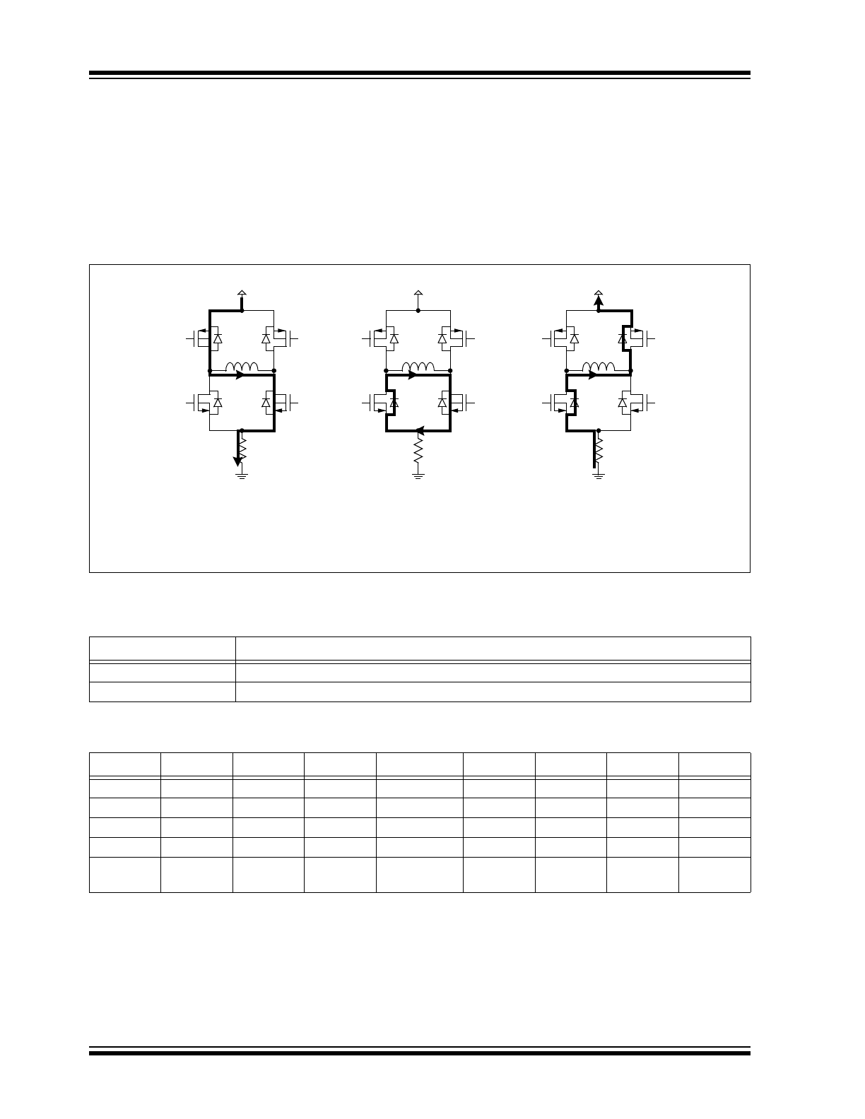
Power Bridge Operation
Each motor winding is driven by an H-type bridge
consisting of two N and two P transistors that allow the
current to flow in both winding directions depending on
the value of the PHASE signal (
Table 3-1
). The
H-bridge can be set in five configurations that are
related to the digital inputs PHASE, I0 and I1 and to the
current sensed. These configurations are shown in
Table 3-2
.
FIGURE 3-1:
Power Bridge Control (PHASE = H/forward).
Legend: a) Bridge ON, b) Source OFF, c) All OFF/Coasting
Note: For PHASE = L/Reverse, invert A and B in drawings.
V
LOAD
Pb
Pa
H
H
L
L
Nb
Na
SENSE
OUTA
OUTB
V
LOAD
Pb
Pa
H
H
L
L
Nb
Na
SENSE
OUTA
OUTB
V
LOAD
Pb
Pa
H
H
L
L
Nb
Na
SENSE
OUTA
OUTB
R
S
R
S
R
S
a)
b)
c)
TABLE 3-1:
CURRENT DIRECTION CONTROL
Phase
Output Current
L
Current flows from OUTxB to OUTxA
H
Current flows from OUTxA to OUTxB
TABLE 3-2:
POWER BRIDGE GATE CONTROL TRUTH TABLE
I0I1
PHASE
Overi
T
OFF
Case/Mode
gna
gpa
gnb
gpb
00/01/10
1
0
0
Forward ON
L
L
H
H
00/01/10
1
x
1
Forward OFF
L
H
H
H
00/01/10
0
0
0
Reverse ON
H
H
L
L
00/01/10
0
x
1
Reverse OFF
H
H
L
H
11
x
x
x
No Current/
Coasting
L
H
L
H
Legend: Bold = Active MOS Transistors, Overi = Overcurrent flag, T
OFF
= Channel T
OFF
State Flag
2010-2013 Microchip Technology Inc.
DS22260C-page 9
MTS62C19A
3.2
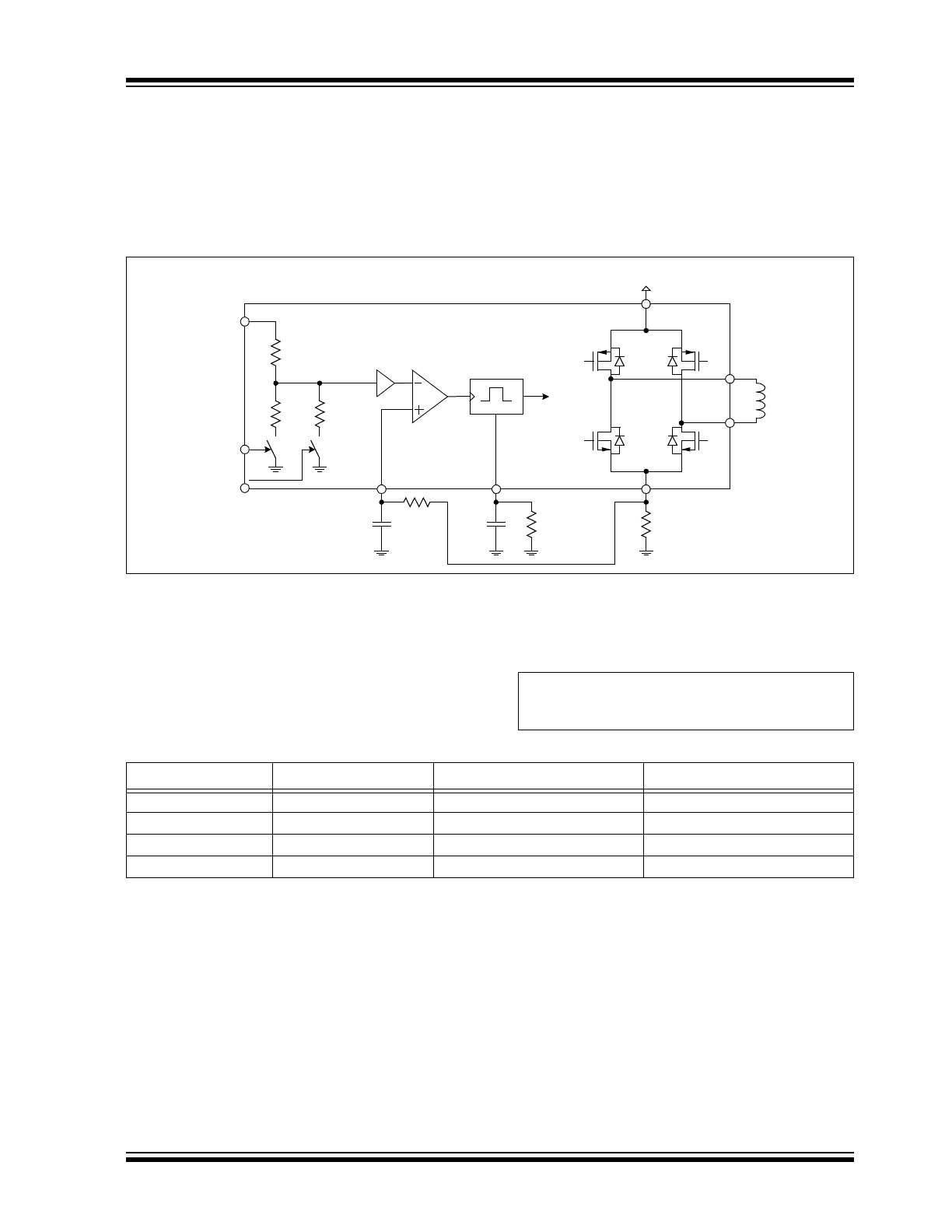
PWM Current Control
The current level in each motor winding is controlled by
a PWM circuit with a fixed T
OFF
time. The load current
flowing in the winding is sensed through an external
sensing resistor R
S
, connected between the power
bridge's source pin SENSE (sources of transistors Na
and Nb) and GND.
FIGURE 3-2:
PWM Current Control Circuit Principle (Channel 1 Shown).
The voltage across R
S
is compared to a fraction of the
reference voltage V
REF
, chosen with the logic input bits
I0 and I1 (
Table 3-3
). The power bridge, and thus the
load current, can also be switched off completely when
both logic inputs are high. Note that any logic input left
unconnected will be treated as a high level (pull-up
resistor).
The maximum trip current for regulation, given for
I0 I1 = 00 is calculated in
Equation 3-1
.
EQUATION 3-1:
V
LOAD
SENSE
V
REF
I0
I1
COMPIN
C
C
R
C
C
t
R
t
R
S
RC
÷10
One-Shot
Source
Disable
Power
Bridge
Pa
Pb
Na
Nb
OUTA
OUTB
I
MAX
V
REF
10
R
S
------------------
=
TABLE 3-3:
CURRENT LEVEL CONTROL TRUTH TABLE
I0
I1
Comp. Trip Voltage
Output Current
0
0
V
TRIP
= 1/10 x V
REF
I
MAX
= V
REF
/10R
S
1
0
V
TRIP
= 1/15 x V
REF
2/3 x I
MAX
= V
REF
/15R
S
0
1
V
TRIP
= 1/30 x V
REF
1/3 x I
MAX
= V
REF
/30R
S
1
1
x
0 (no current)
MTS62C19A
DS22260C-page 10
2010-2013 Microchip Technology Inc.
When the maximum allowed current is reached, the
bridge source is turned off during a fixed period T
OFF
(typically 50 µs) given by a non-retriggerable pulse
generator and the external timing components R
t
(20k – 100 k
range) and C
t
(100 pF – 1000 pF
range):
EQUATION 3-2:
During T
OFF
the winding current decreases. When the
driver is re-enabled, the winding current increases
again until it reaches the threshold, and the cycle
repeats itself, maintaining the load current at the
desired level.
FIGURE 3-3:
PWM Output Current
Waveform.
3.3
Circuit Protection
A thermal protection circuitry turns off all drivers when
the junction temperature exceeds a safe operating limit
of +170°C (typical). This protects the devices from
failure due to excessive heating. Despite this thermal
protection, output short circuits are not permitted. The
output drivers are re-enabled once junction
temperature has dropped below +145°C (typical).
FIGURE 3-4:
Thermal Shutdown Output
vs. Temperature Showing Hysteresis.
An undervoltage lockout circuit protects the
MTS62C19A from potential shoot-through currents
when the load supply voltage is applied prior to the
logic supply voltage. The power bridge and all outputs
are disabled if V
LOGIC
is smaller than 4V.
With this protection feature, the circuit will withstand
any order of turn-on or turn-off of the supply voltages
V
LOGIC
and V
LOAD.
Normal dV/dt values are assumed.
T
OFF
1.1
R
t
C
t
=
PHASE
I
OUT
+
0
-
I
OUT
t
off
t
d
t
on
1
0
+170°C
+145°C
thshtd_en