

2015 Microchip Technology Inc.
DS20005359A-page 1
MTD6508
Features
• 180° Sinusoidal Drive for High Efficiency and Low
Acoustic Noise
• Position Sensorless BLDC Drivers
(no Hall Effect Sensor required)
• Integrated Power Transistors
• Supports 2V to 5.5V Power Supplies
• Variable Programming Resistor (R
PROG
) Setting
to fit Motor Constant (K
M
) Range from 3.25 mV/
Hz to 52 mV/Hz
• Speed Control through Power Supply Modulation
(PSM) and/or Pulse-Width Modulation (PWM)
• Built-in Frequency Generator: FG, FG/3 Output
Signal (FG/2 and FG/6 Option are available upon
request)
• Output PWM Slew Rate Control Programmable
with an External Resistor for Start-up
(Adjustable version)
• Phase Target Selection for Regulation
(Adjustable Version)
• Start-up Strength Selection (Adjustable Version)
• Start-up Output Current Controlled by PWM
• Output Current Soft Start
• Built-in Lock-up Protection and Automatic
Recovery Circuit
• Built-in Overcurrent Limitation
• Built-in Thermal Shutdown Protection
• Built-in Overvoltage Protection
• Low Minimal Start-up Speed for Low-Speed
Operation
• Packages:
- 10-Lead 3 mm x 3 mm x 0.5 mm UDFN
- 16-Lead 4 mm x 4 mm x 0.5 mm UQFN
(Adjustable version)
Applications
• Notebook CPU Cooling Fans
• 5V 3-Phase BLDC Motors
Description
The MTD6508 device is a 3-phase, full-wave
sensorless driver for brushless DC (BLDC) motors. It
features a 180° sinusoidal drive, high torque output and
silent drive. With adaptive features, parameters and a
wide range of power supplies (2V to 5.5V), the
MTD6508 is intended to cover a broad range of motor
characteristics while requiring minimum external
components. Speed control can be achieved through
either power supply modulation (PSM) or pulse-width
modulation (PWM).
Compact packaging and a minimal bill of materials
make the MTD6508 device extremely cost-efficient in
fan applications. For example, the CPU cooling fans in
notebook computers require designs that provide low
acoustic noise, low mechanical vibration and are highly
efficient. The frequency generator (FG) output enables
precision speed control in closed-loop applications.
The MTD6508 device includes Lock-up Protection
mode to turn off the output current when the motor is in
a lock condition, with an automatic recovery feature to
restart the fan when the lock condition is removed.
Motor overcurrent limitation and thermal shutdown
protection are included for safety-enhanced operations.
The MTD6508 is available in compact, thermally-
enhanced, 10-Lead 3 mm x 3 mm x 0.5 mm UDFN
packages and 16-Lead 4 mm x 4 mm x 0.5 mm
UQFN packages.
3-Phase Sinusoidal Sensorless Brushless DC Fan Motor Driver
MTD6508
DS20005359A-page 2
2015 Microchip Technology Inc.
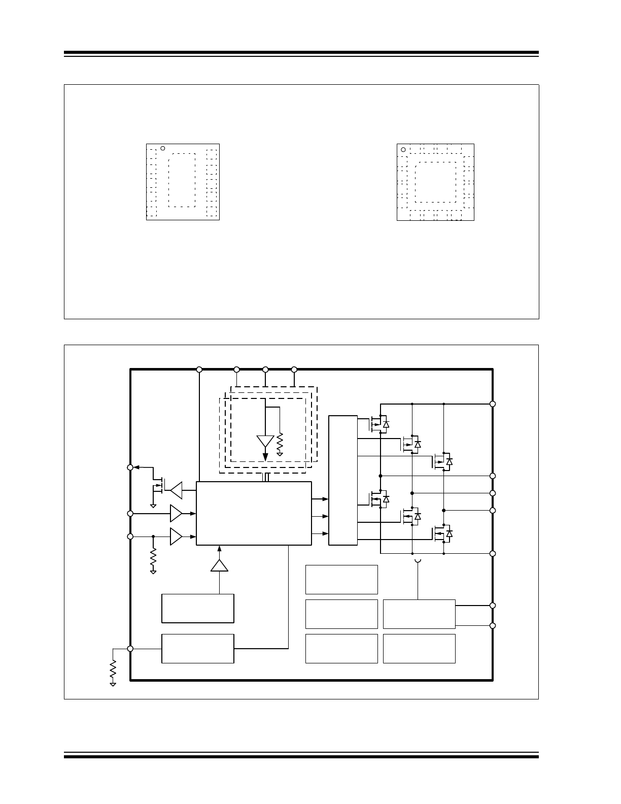
Package Types
Functional Block Diagram
*Includes Exposed Thermal Pad (EP); see
Table 3-1
.
MTD6508
4x4 UQFN-16*
MTD6508
3x3 UDFN-10*
Note: The DIR, SS and RT pins that are not available on UDFN-10 Package are internally pulled down. SR1 and
SR2 are connected by a fixed internal resistor (25 kΩ).
2
V
BIAS
OUT2
FG
RT
PWM
GND
FG3_SEL
OUT1
GND
OUT3
V
DD
DIR
SR
1
SR
2
SS
R
PROG
EP
16
1
15 14 13
3
4
12
11
10
9
5
6
7
8
17
V
BIAS
R
PROG
OUT1
FG3_SEL
V
DD
1
2
3
4
10
9
8
7 OUT3
PWM
FG
EP
11
5
6
OUT2
GND
Thermal
Protection
V
BIAS
OUT1
OUT2
CPU + Peripherals
PWM
FG
OUT3
V
DD
Short-Circuit
Protection
O
u
tput
D
ri
ve C
irc
ui
t
Motor Phase
Detection Circuit
Overcurrent
Protection
GND
Nonvolatile
Memory
R
PROG
Sense
R
PROG
Adju stable K
M
Slew Rate
Control
SR1
SR2
RT
SS
DIR
FG3_SEL
2015 Microchip Technology Inc.
DS20005359A-page 3
MTD6508
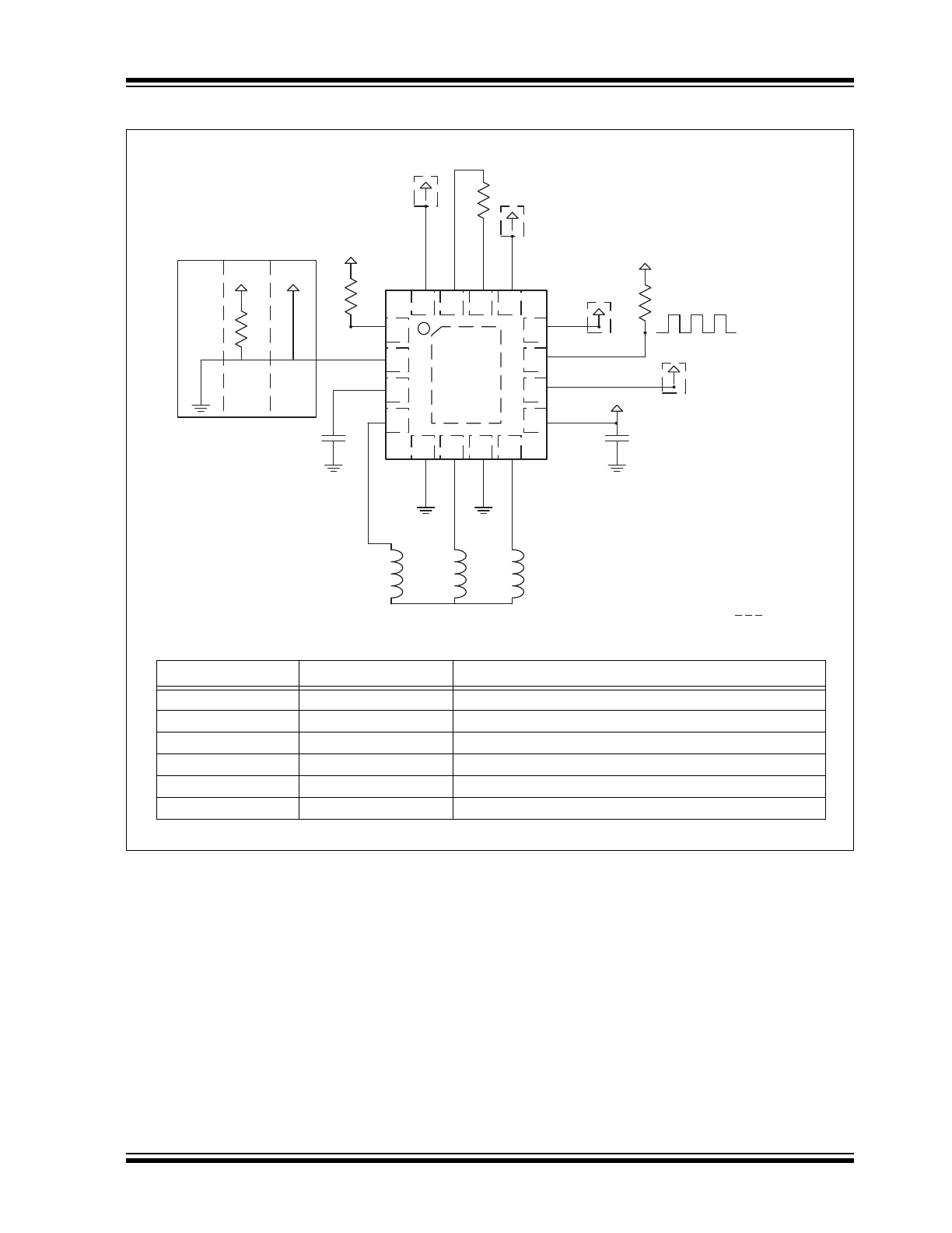
Typical Application
FG
V
BIAS
OUT2
OU
T
1
GN
D
OU
T
3
FG3_SEL
PWM
R
PR
O
G
C1
V
DD
C2
V
LOGIC
R
FG
K
M
0
K
M
3
K
M
1, 2
R
PROG
V
BIAS
V
BIAS
RT
DI
R
SR1
SR2
SS
R
SR
V
DD
PWM input
(1-100 kHz)
GN
D
V
LOGIC
= V
BIAS
or V
DD
= Optional
V
LOGIC
R
PW
M
V
LOGIC
V
LOGIC
V
LOGIC
V
BIAS
1
EP
17
16
15
14
13
5
6
7
8
2
3
4
12
11
10
9
Legend
Recommended External Components for Typical Application
Element
Type/Value
Comment
C1
1 µF
Connect as close as possible to IC input pin
C2
1 µF
Connect as close as possible to IC input pin
R
FG
10 kΩ
Connect to V
logic
on microcontroller side (FG Pull-Up)
R
PWM
100 kΩ
Connect to V
logic
on microcontroller side (PWM Pull-Up)
R
PROG
3.9 kΩ or 24 kΩ
Select appropriate programming resistor value, see
Table 4-1
R
SR
4.7 kΩ-47 kΩ
Select appropriate output PWM slew rate, see
Table 4-2

MTD6508
DS20005359A-page 4
2015 Microchip Technology Inc.
NOTES:
2015 Microchip Technology Inc.
DS20005359A-page 5
MTD6508
1.0
ELECTRICAL
CHARACTERISTICS
Absolute Maximum Ratings†
Power Supply Voltage (V
DD_MAX
) ...................... -0.7 to +7.0V
Maximum Output Voltage (V
OUT_MAX
) ............... -0.7 to +7.0V
Maximum Output Current
(I
OUT_MAX
)
(
1
)
....................1000 mA
FG Maximum Output Voltage (V
FG_MAX
) ........... -0.7 to +7.0V
FG Maximum Output Current (I
FG_MAX
) ......................5.0 mA
V
BIAS
Maximum Voltage (V
BIAS_MAX
) ................ -0.7 to +4.0V
PWM Maximum Voltage (V
PWM_MAX
) ................ -0.7 to +7.0V
Allowable Power Dissipation (P
D_MAX
)
(
2
)
........................1.5W
Maximum Junction Temperature (T
J
).......................... +150°C
ESD protection on all pins
2 kV
† Notice: Stresses above those listed under “Maximum
Ratings” may cause permanent damage to the device.
This is a stress rating only, and functional operation of
the device at those or any other conditions above those
indicated in the operational listings of this specification
is not implied. Exposure to maximum rating conditions
for extended periods may affect device reliability.
Note 1: I
OUT
is also internally limited, according
to the limits defined in the
Electrical
Characteristics
table.
2: Reference Printed Circuit Board (PCB)
according to JEDEC standard EIA/JESD
51-9.
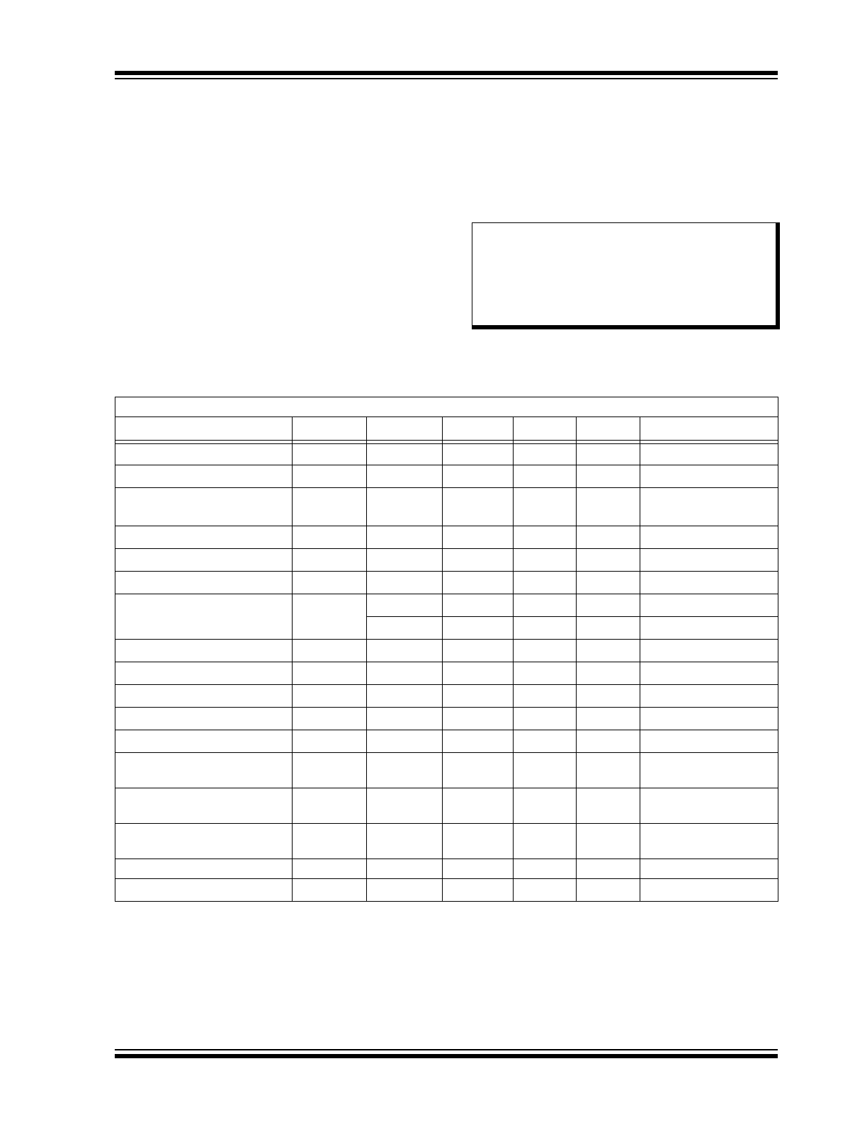
ELECTRICAL CHARACTERISTICS
Electrical Specifications: Unless otherwise specified, all limits are established for V
DD
= 2.0V to 5.5V, T
A
= +25°C
Parameters
Sym.
Min.
Typ.
Max.
Units
Conditions
Power Supply Voltage
V
DD
2
—
5.5
V
Power Supply Current
I
VDD
—
5
10
mA
V
DD
= 5V
Standby Current
I
VDD_STB
—
15
25
µA
PWM = 0V, V
DD
= 5V
(Standby mode)
OUTX High Resistance
R
ON(H)
—
0.75
—
Ω
I
OUT
= 0.5A, V
DD
= 5V
OUTX Low Resistance
R
ON(L)
—
0.75
—
Ω
I
OUT
= 0.5A, V
DD
= 5V
OUTX Total Resistance
R
ON(H+L)
—
1.5
—
Ω
I
OUT
= 0.5A, V
DD
= 5V
V
BIAS
Internal
Supply Voltage
V
BIAS
—
3
—
V
V
DD
= 3.2V to 5.5V
—
V
DD
– 0.2
—
V
V
DD
< 3.2V
PWM Input Frequency
f
PWM
1
—
100
kHz
PWM Input H Level
V
PWM_H
0.55
V
DD
—
V
DD
V
V
DD
4.5V
PWM Input L Level
V
PWM_L
0
—
0.2
V
DD
V
V
DD
4.5V
FG3_SEL Input H Level
V
FG3_SEL_H
V
BIAS
– 0.5
—
V
BIAS
V
V
DD
4.5V
FG3_SEL Input L Level
V
FG3_SEL_L
0
—
0.2
V
DD
V
V
DD
4.5V
FG Output Pin Low-Level
Voltage
V
OL_FG
—
—
0.25
V
I
FG
= -1 mA
FG Output Pin Leakage
Current
I
LH_FG
-10
—
10
µA
V
FG
= 5.5V
Lock Protection
Operating Time
T
RUN
—
0.5
1
s
Lock Protection Waiting Time
T
WAIT
5
5.5
6
s
Note 1
Overcurrent Protection
I
OC_MOT
—
750
—
mA
Note 2
Note 1:
Related to the internal oscillator frequency (see
Figure 2-1
)
2:
750 mA is the standard option for MTD6508. Additional overcurrent protection levels are available upon
request. Please contact factory for different overcurrent protection values.
MTD6508
DS20005359A-page 6
2015 Microchip Technology Inc.
Overvoltage Protection
V
OV
—
7.2
—
V
Short Protection on High Side
I
OC_SW_H
—
2.57
—
A
Short Protection on Low Side
I
OC_SW_L
—
-2.83
—
A
Thermal Shutdown
T
SD
—
170
—
°C
Thermal Shutdown Hysteresis
T
SD_HYS
—
25
—
°C
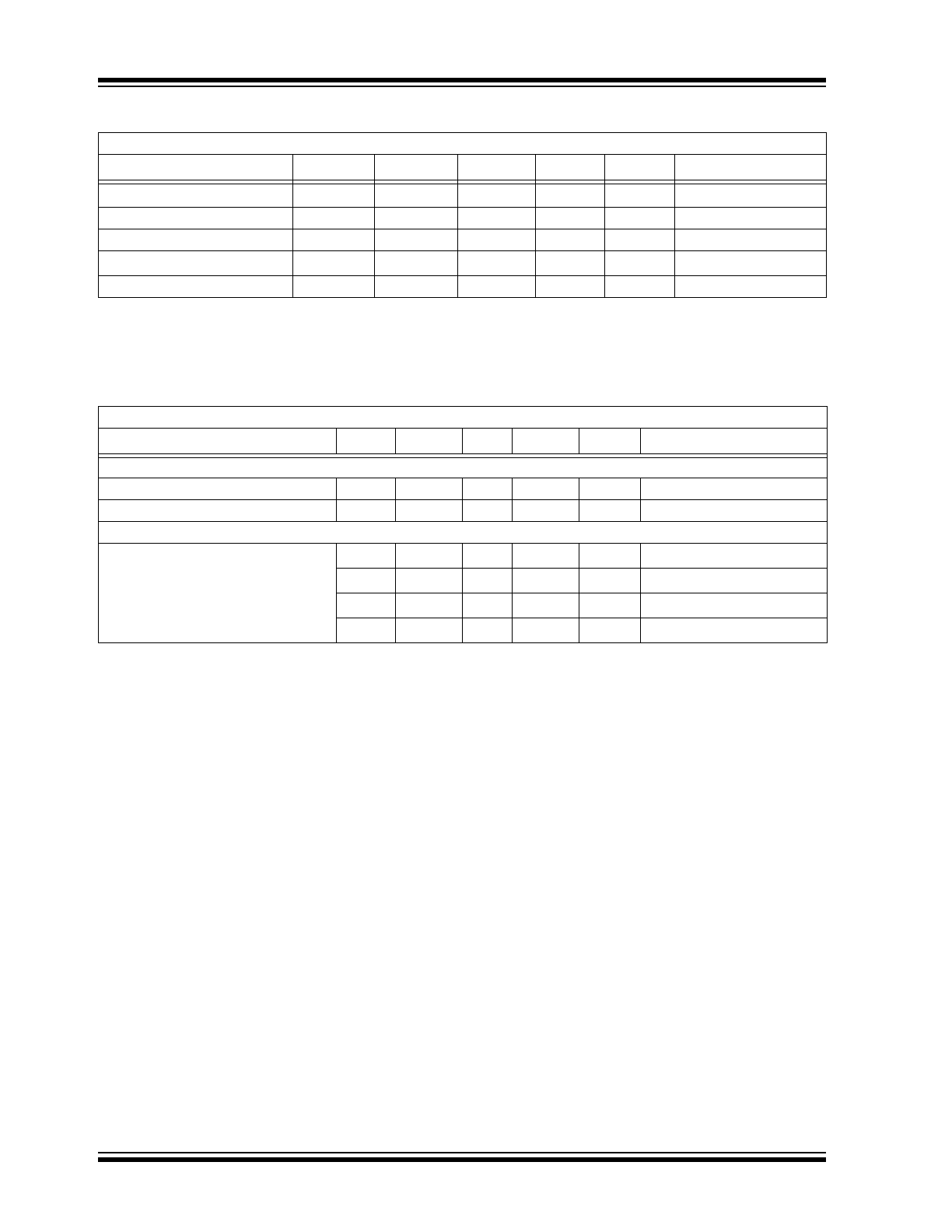
TEMPERATURE SPECIFICATIONS
Electrical Specifications: Unless otherwise specified, all limits are established for V
DD
= 2.0V to 5.5V, T
A
= +25°C.
Parameters
Sym.
Min.
Typ.
Max.
Units
Conditions
Temperature Ranges
Operating Temperature
T
OPR
-40
—
+125
°C
Storage Temperature Range
T
STG
-55
—
+150
°C
Thermal Package Resistances
Thermal Resistance, 10L-UDFN, 3x3
JA
—
68
—
°C/W
JC
—
11
—
°C/W
Thermal Resistance, 16L-UQFN, 4x4
JA
—
31.8
—
°C/W
JC
—
10
—
°C/W
ELECTRICAL CHARACTERISTICS (CONTINUED)
Electrical Specifications: Unless otherwise specified, all limits are established for V
DD
= 2.0V to 5.5V, T
A
= +25°C
Parameters
Sym.
Min.
Typ.
Max.
Units
Conditions
Note 1:
Related to the internal oscillator frequency (see
Figure 2-1
)
2:
750 mA is the standard option for MTD6508. Additional overcurrent protection levels are available upon
request. Please contact factory for different overcurrent protection values.
2015 Microchip Technology Inc.
DS20005359A-page 7
MTD6508
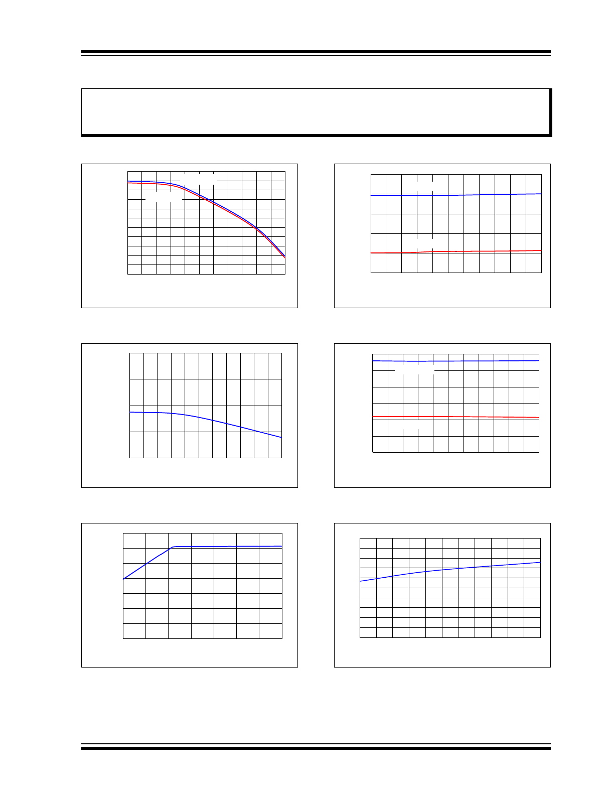
2.0
TYPICAL PERFORMANCE CURVES
Note: Unless indicated, T
A
= +25°C, V
DD
= 2.0V to 5.5V, OUT1, 2, 3 and PWM open.
FIGURE 2-1:
Oscillator Frequency
Deviation vs. Temperature.
FIGURE 2-2:
Internal Regulated Voltage
(V
BIAS
) vs Temperature.
FIGURE 2-3:
Internal Regulated Voltage
(V
BIAS
) vs Supply Voltage (V
DD
).
FIGURE 2-4:
Inputs (PWM) V
IL
vs.
Temperature.
FIGURE 2-5:
Inputs (PWM) V
IH
vs.
Temperature.
FIGURE 2-6:
Outputs R
ON
High-Side
Resistance vs. Temperature.
Note:
The graphs and tables provided following this note are a statistical summary based on a limited number of
samples and are provided for informational purposes only. The performance characteristics listed herein
are not tested or guaranteed. In some graphs or tables, the data presented may be outside the specified
operating range (e.g., outside specified power supply range) and therefore outside the warranted range.
-4.5
-4
-3.5
-3
-2.5
-2
-1.5
-1
-0.5
0
0.5
1
-40 -25 -10 5
20 35 50 65 80 95 110 125
Oscillator Frequeny
Deviation
(%
)
Temperature (°C)
V
DD
= 5.5V
V
DD
= 2V
3
3.02
3.04
3.06
3.08
-40 -25 -10 5
20 35 50 65 80 95 110 125
V
BIA
S
(V)
Temperature (°C)
V
DD
= 5.5V
0
0.5
1
1.5
2
2.5
3
3.5
2.0
2.5
3.0
3.5
4.0
4.5
5.0
5.5
V
BIA
S
(V)
V
DD
(V)
0
0.5
1
1.5
2
2.5
-40 -25 -10
5
20
35
50
65
80
95 110 125
PWM V
IL
(V)
Temperature (°C)
VDD = 5.5
VDD = 5.5
V
DD
= 5.5V
V
DD
= 2V
0
0.5
1
1.5
2
2.5
3
-40 -25 -10
5
20
35
50
65
80
95 110 125
PWM V
IH
(V)
Temperature (°C)
V
DD
= 5.5V
V
DD
= 2V
0
0.1
0.2
0.3
0.4
0.5
0.6
0.7
0.8
0.9
1
-40
-25
-10
5
20
35
50
65
80
95
110 125
RON High Side (
ȍ
)
Temperature (°C)
V
DD
= 5.5V
MTD6508
DS20005359A-page 8
2015 Microchip Technology Inc.
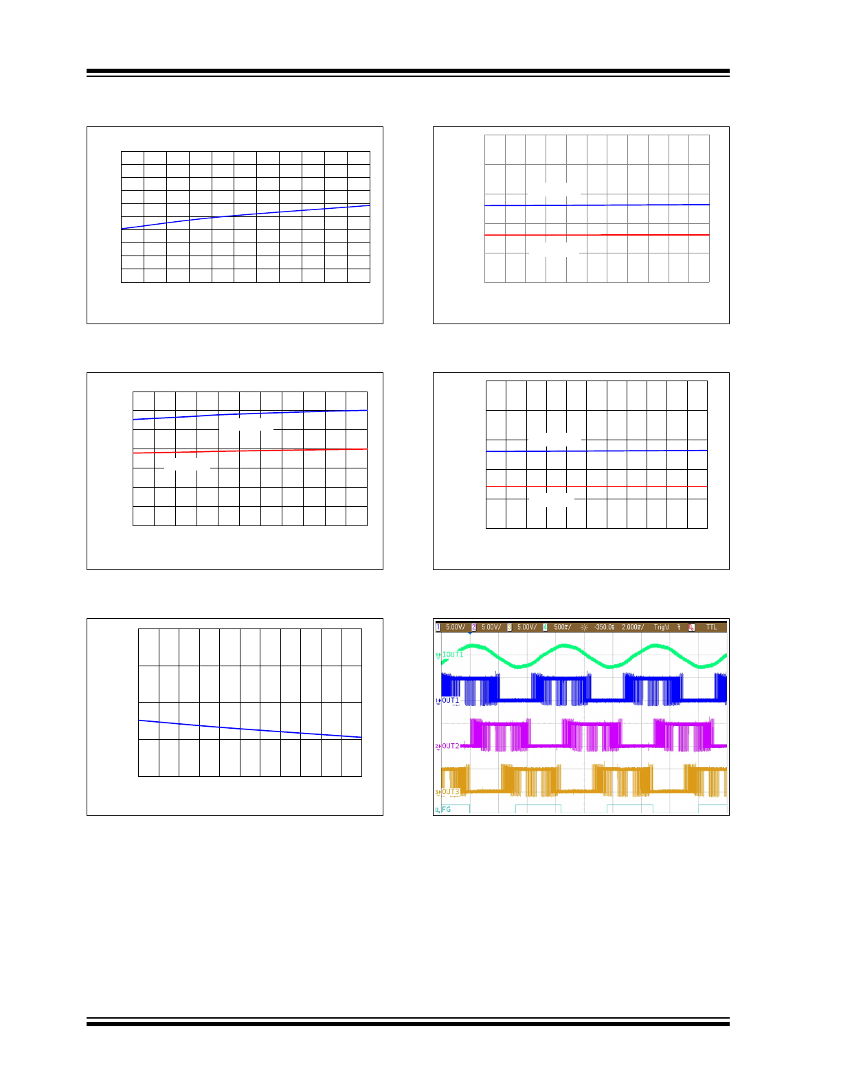
Note: Unless indicated, T
A
= +25°C, V
DD
= 2.0V to 5.5V, OUT1, 2, 3 and PWM open.
FIGURE 2-7:
Outputs R
ON
Low-Side
Resistance vs. Temperature.
FIGURE 2-8:
Supply Current vs.
Temperature.
FIGURE 2-9:
Standby Current vs.
Temperature.
FIGURE 2-10:
DIR, SS and RT Pins V
IL
(V)
vs. Temperature.
FIGURE 2-11:
DIR, SS and RT Pins V
IH
(V)
vs. Temperature.
FIGURE 2-12:
Typical Outputs on Closed
Loop.
0
0.1
0.2
0.3
0.4
0.5
0.6
0.7
0.8
0.9
1
-40
-25
-10
5
20
35
50
65
80
95
110 125
RON Low
Side
(ȍ
)
Temperature (°C)
V
DD
= 5.5V
0
1
2
3
4
5
6
7
-40 -25 -10
5
20
35
50
65
80
95 110 125
I
VDD
Current (mA)
Temperature (°C)
V
DD
= 2V
V
DD
= 5.5V
0
10
20
30
40
-40 -25 -10
5
20 35 50 65 80 95 110 125
I
VDD_STB
Current (μA)
Temperature (°C)
V
DD
= 5.5V
0
0.5
1
1.5
2
2.5
-40 -25 -10
5
20 35 50 65 80 95 110 125
DIR, SS
and R
T Pins V
IL
(V)
Temperature (°C)
V
DD
= 5.5V
V
DD
= 2V
0
0.5
1
1.5
2
2.5
-40 -25 -10
5
20 35 50 65 80 95 110 125
DIR, SS and RT Pins
V
IH
(V)
Temperature (°C)
V
DD
= 5.5V
V
DD
= 2V
2015 Microchip Technology Inc.
DS20005359A-page 9
MTD6508
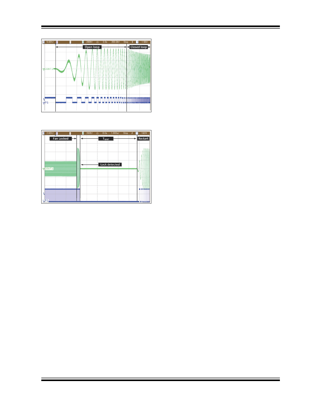
FIGURE 2-13:
Typical Output Current on
Start-up.
FIGURE 2-14:
Typical Outputs on Locked
Motor While Running.
MTD6508
DS20005359A-page 10
2015 Microchip Technology Inc.
3.0
PIN DESCRIPTIONS
The descriptions of the pins are listed in
Table 3-1
.
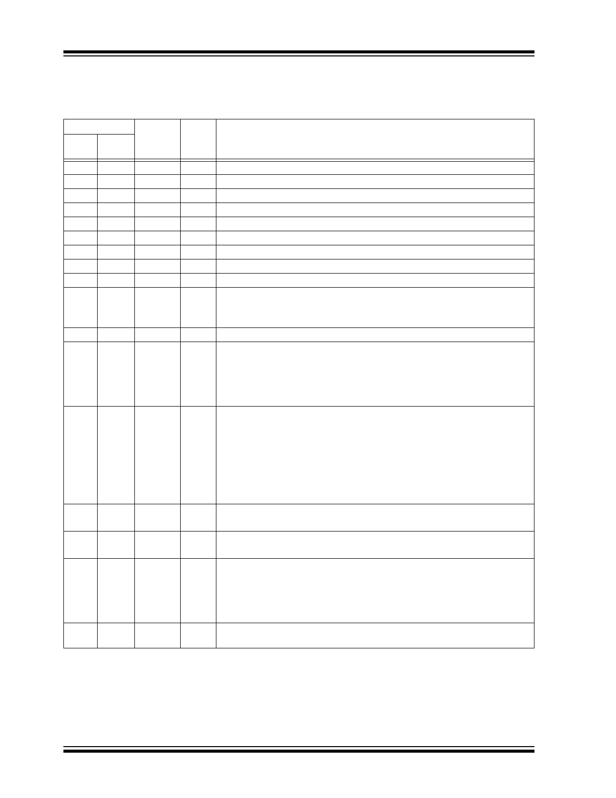
TABLE 3-1:
PIN FUNCTION TABLE
MTD6508
Name
Type
Function
3x3
UDFN
4x4
UQFN
1
1
FG
O
Motor Speed Indication Output Pin
2
2
R
PROG
I
K
M
Parameter Setting with External Resistors Pin (do not leave floating)
3
3
V
BIAS
O
3V Internal Regulator Output Pin (for decoupling only)
5
4
OUT2
O
Single-Phase Coil Output Pin
6
5
GND
P
Negative Voltage Supply Pin (ground)
4
6
OUT1
O
Single-Phase Coil Output Pin
6
7
GND
P
Negative Voltage Supply Pin (ground)
7
8
OUT3
O
Single-Phase Coil Output Pin
8
9
V
DD
P
Positive Voltage Supply for Motor Driver Pin
9
10
FG3_SEL
I
FG Frequency Divider Selection Pin:
- FG signal divided by three: connect this pin to V
BIAS
- FG normal signal: connect this pin to GND or leave floating
10
11
PWM
I
PWM Input Signal for Close-Loop Speed Control Pin (do not leave floating)
—
12
RT
I
Regulation Target Pin – phase target selection for regulation:
- Normal regulation: connect this pin to GND or leave floating
- Low load regulation: connect this pin to V
BIAS
or V
DD
- Pin not available on UDFN-10 option; selection fixed to normal
regulation
—
13
SS
I
Strong Start Pin – start-up strength selection:
- Soft open-loop start-up (reduced current) – during the start-up open-
loop, the output amplitude is defined by the input PWM duty cycle:
connect this pin to GND or leave floating
- Strong open-loop start-up – during the start-up open-loop, the output
amplitude is fixed to 100%: connect this pin to V
BIAS
or V
DD
- Pin not available on UDFN-10 option; selection fixed to soft
open-loop start-up
—
14
SR2
O
Start-up Output PWM Slew Rate Control Pin 2 (High side)
- Pin not available on UDFN-10 option; selection fixed to 250 ns (25 kΩ)
—
15
SR1
I
Start-up Output PWM Slew Rate Control Pin 1 (Low side)
- Pin not available on UDFN-10 option; selection fixed to 250 ns (25 kΩ)
—
16
DIR
I
Motor Rotation Direction Pin (DIR function):
- Forward direction: connect this pin to GND or leave floating
- Reverse direction: connect this pin to V
BIAS
or V
DD
- Pin not available on UDFN-10 option; selection fixed to forward
direction
11
17
EP
N/A
Exposed Pad Pin; connect to ground plane on the PCB for enhanced thermal
performance
Note:
I = Input, O = Output, P = Power