
© 2011 Microchip Technology Inc.
DS25003B-page 1
Features:
• Position Sensorless BLDC Drivers
(No Hall Sensor Required)
• 180° Sinusoidal Drive, for High Efficiency and Low
Acoustic Noise
• Support 2V to 5.5V Power Supplies
• Direction Control:
- Forward direction: connect DIR pin to GND or
leave floating
- Reverse direction: connect DIR pin to V
DD
• Speed Control through Power Supply Modulation
(PSM) and/or Pulse-Width Modulation (PWM)
• Built-in Frequency Generator (FG Output Signal)
• Built-in Lock-up Protection and Automatic
Recovery Circuit (External Capacitor not
Necessary)
• Built-in Over Current Limitation
• Built-in Thermal Shutdown Protection
• No External Tuning Required
• Available Packages:
- 3 mm x 3 mm TDFN-10
Applications:
• Notebook CPU Cooling Fans
• 5V 3-Phase Brushless DC Motors
Description:
The MTD6502B device is a 3-phase full-wave driver for
brushless sensorless DC motors. It features 180°
sinusoidal drive, high torque output and silent drive.
With adaptive features, parameters and a wide range
of power-supplies (2V to 5.5V), the MTD6502B device
is intended to cover a wide range of motor
characteristics, while requiring minimum external
components. Speed control can be achieved through
either power supply modulation or pulse-width
modulation (using the PWM digital input pin).
With the compact packaging and minimum bill-of-
material (integrated power transistors, no Hall sensor,
no external tuning), the MTD6502B is best suited for
low-cost fan applications requiring high efficiency and
low acoustic noise, such as notebook CPU cooling
fans. Frequency generator (FG) output enables the
precision speed control in closed-loop applications.
The MTD6502B driver includes a lock-up protection
mode, which turns off the output current when the
motor is under lock condition, and an automatic
recovery that enables the fan to run when the lock
condition is removed. The motor overcurrent limitation
and thermal-shutdown protection are included for
safety-enhanced operations.
The MTD6502B is available in a compact thermally-
enhanced 3 mm x 3 mm TDFN package.
Package Types
MTD6502B
3x3 TDFN*
V
DD
GND
OUT1
DIR
V
CC
1
2
3
4
9
8
7
6
PWM
FG
* Includes Exposed Thermal Pad (EP); see
Table 2-1
.
EP
11
5
10
OUT2
OUT3
GND
5V 3-Phase BLDC Sinusoidal Sensorless Fan Motor Driver
MTD6502B
MTD6502B
DS25003B-page 2
© 2011 Microchip Technology Inc.
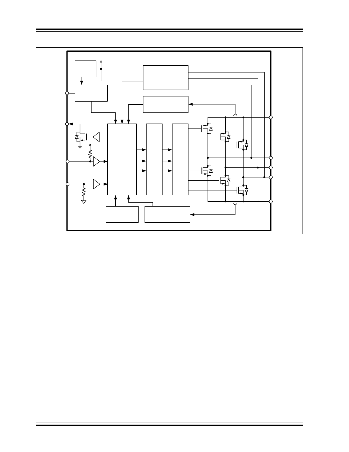
Functional Block Diagram
Thermal
protection
V
DD
OUT1
OUT2
Controller
PWM
OUT3
V
CC
Short-circuit
protection
O
utp
u
t Dri
ve
Ci
rcu
it
Motor Phase
Detection Circuit
Over-current
protection
So
ft Sw
itc
h
in
g
D
riv
e
V
CC
Regulator
V
REF
GND
V
CC
DIR
FG
© 2011 Microchip Technology Inc.
DS25003B-page 3
MTD6502B
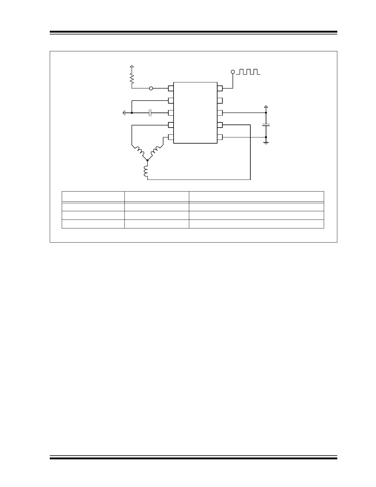
Typical Application
Recommended External Components for Typical Application
Element
Type/Value
Comment
C1
≥1 µF
Connect as close as possible to IC input pins
C2
≥1 µF
Connect as close as possible to IC input pins
R1
≥10 kΩ
Connect to Vlogic on microcontroller side
OUT1
GND
OUT2
GND
DIR
PWM
OUT3
1
2
4
5
6
7
9
10
V
DD
V
CC
3
8
R1
MCU Side
(Vlogic)
C1
C2
PWM Input
(1-100 kHz)
FG
V
CC
MT
D6
50
2B

MTD6502B
DS25003B-page 4
© 2011 Microchip Technology Inc.
NOTES:
© 2011 Microchip Technology Inc.
DS25003B-page 5
MTD6502B
1.0
ELECTRICAL
CHARACTERISTICS
Absolute Maximum Ratings†
Power Supply Voltage (V
CC_MAX
) ...................... -0.7 to +7.0V
Maximum Output Voltage (V
OUT_MAX
) ............... -0.7 to +7.0V
Maximum Output Current
(
2
)
(I
OUT_MAX
) ....................1000 mA
FG Maximum Output Voltage (V
FG_MAX
) ........... -0.7 to +7.0V
FG Maximum Output Current (I
FG_MAX
)
.....................5.0 mA
V
DD
Maximum Voltage (V
DD_MAX
) ..................... -0.7 to +4.0V
PWM Maximum Voltage (V
PWM_MAX
) ................ -0.7 to +7.0V
Allowable Power Dissipation
(
2
)
(P
D_MAX
).........................1.5W
Maximum Junction Temperature (T
J
).......................... +150°C
† Notice:
Stresses above those listed under “Maximum
Ratings” may cause permanent damage to the device. This is
a stress rating only and functional operation of the device at
those or any other conditions above those indicated in the
operational listings of this specification is not implied.
Exposure to maximum rating conditions for extended periods
may affect device reliability.
Note 1:
Reference PCB, according to JEDEC
standard EIA/JESD 51-9.
2:
I
OUT
is also internally limited, according
to limits defined in the
Electrical
Characteristics
.
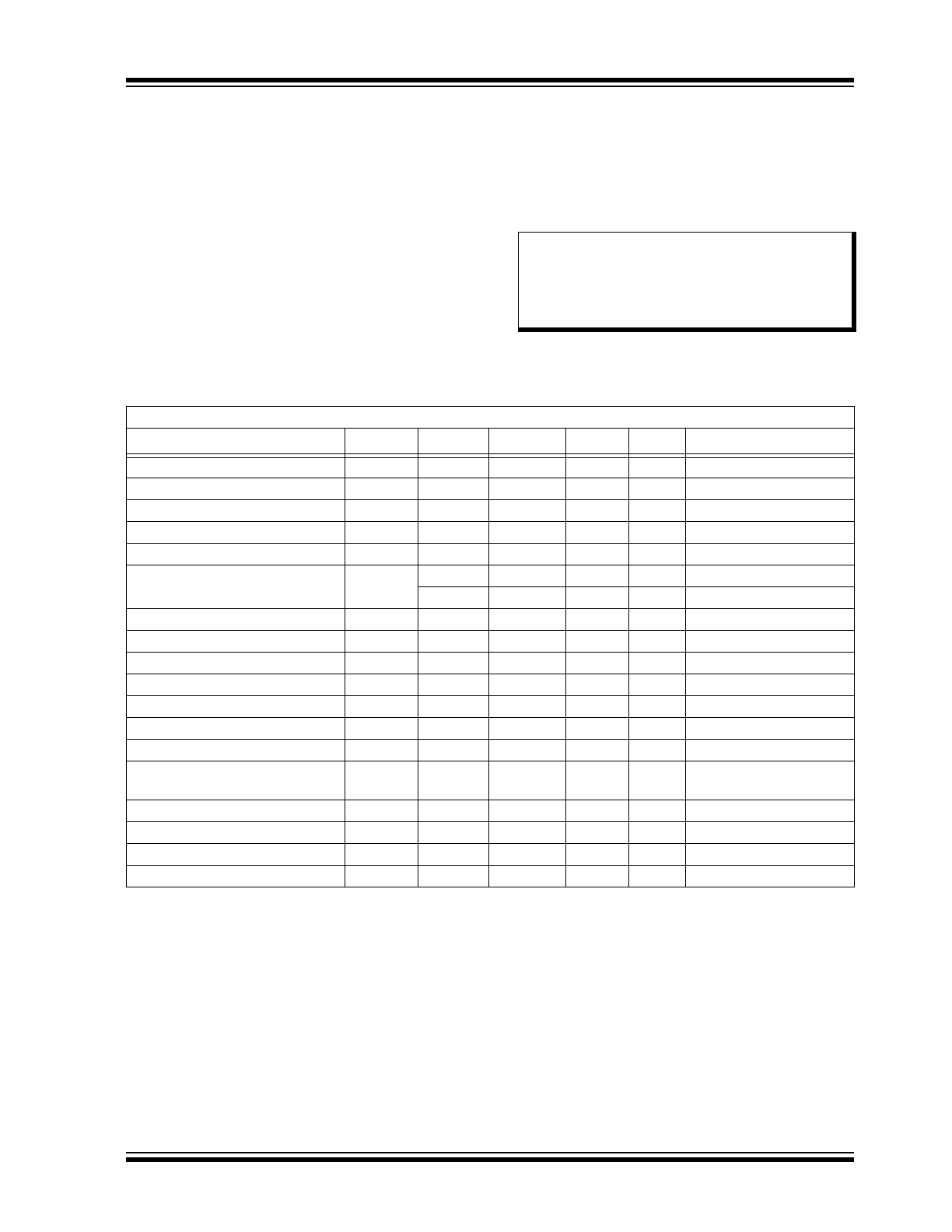
ELECTRICAL CHARACTERISTICS
Electrical Specifications:
Unless otherwise specified, all limits are established for T
A
= +25°C
Parameters
Sym
Min
Typ
Max
Units
Conditions
Power Supply Voltage
V
CC
2
—
5.5
V
Power Supply Current
I
VCC
—
50
—
µA
PWM = 0, V
CC
= 5V
OUTx High Resistance
R
ON(H)
—
0.75
1
Ω
I
OUT
= 0.5A, V
CC
= 5V
OUTx Low Resistance
R
ON(L)
—
0.75
1
Ω
I
OUT
= 0.5A, V
CC
= 5V
OUTx Total Resistance
R
ON(H+L)
—
1.5
2
Ω
I
OUT
= 0.5A, V
CC
= 5V
V
DD
Output Voltage
V
DD
—
3
—
V
V
CC
= 3.3V to 5.5V
—
V
CC
– 0.2
—
V
V
CC
< 3.3V
PWM Input Frequency
f
PWM
1
—
100
kHz
PWM Input H Level
V
PWM_H
0.55*V
CC
—
V
CC
V
PWM Input L Level
V
PWM_L
0
—
0.2*V
CC
V
PWM Internal Pull-Up Current
I
PWM_L
—
—
55
µA
PWM = 0
DIR Internal Pull-Down Current
I
DIR
—
20
—
µA
FG Output Pin Low Level Voltage
V
OL_FG
—
—
0.25
V
I
FG
= -1 mA
FG Output Pin Leakage Current
I
LH_FG
—
—
10
µA
V
FG
= 5.5V
Lock Protection
Operating Time
T
RUN
—
0.5
—
s
Lock Protection Waiting Time
T
WAIT
4.5
5
5.5
s
Overcurrent Protection
I
OC_MOT
—
750
—
mA
Thermal Shutdown
T
SD
—
170
—
°C
Thermal Shutdown Hysteresis
T
SD_HYS
—
25
—
°C
MTD6502B
DS25003B-page 6
© 2011 Microchip Technology Inc.
TEMPERATURE SPECIFICATIONS
Electrical Specifications:
Unless otherwise specified, all limits are established for V
CC
= 5.0V, T
A
= +25°C
Parameters
Sym
Min
Typ
Max
Units
Conditions
Temperature Ranges
Operating Temperature
T
OPR
-40
—
+125
°C
Storage Temperature Range
T
STG
-55
—
+150
°C
Thermal Package Resistances
Thermal Resistance, 10L-TDFN
θ
JA
—
68
—
°C/W
© 2011 Microchip Technology Inc.
DS25003B-page 7
MTD6502B
2.0
PIN DESCRIPTIONS
The descriptions of the pins are listed in
Table 2-1
.
TABLE 2-1:
MTD6502B PIN FUNCTION TABLE
MTD6502B
3x3 TDFN
Type
Name
Function
1
O
FG
Motor speed indication output
2, 6
—
GND
Negative voltage supply (ground)
3
—
V
DD
Internal regulator output (for decoupling only)
4
O
OUT1
Single phase coil output pin
5
O
OUT2
Single phase coil output pin
7
O
OUT3
Single phase coil output pin
8
—
V
CC
Positive voltage supply for motor driver
9
I
DIR
Motor Rotation Direction:
- Forward direction: connect pin to GND or leave floating
- Reverse direction: connect pin to V
DD
10
I
PWM
PWM input signal for speed control
11
—
EP
Exposed Thermal Pad (EP)
Legend:
I = Input; O = Output

MTD6502B
DS25003B-page 8
© 2011 Microchip Technology Inc.
NOTES:
© 2011 Microchip Technology Inc.
DS25003B-page 9
MTD6502B
3.0
FUNCTIONAL DESCRIPTION
The MTD6502B generates a full-wave signal to drive a
3-phase sensorless BLDC motor. High efficiency and
low-power consumption are achieved due to the CMOS
transistors and synchronous rectification drive type.
3.1
Speed Control
The rotational speed of the motor can be controlled
either through the PWM digital input signal, or by acting
directly on the power supply (V
CC
). When the PWM
signal is High (or left open), the motor rotates at full
speed. When the PWM signal is Low, the motor is
stopped (and the IC outputs are set to high-
impedance). By changing the PWM duty cycle, the
speed can be adjusted. Notice that the PWM frequency
has no special meaning for the motor speed and is
asynchronous with the activation of the output
transistors. Thus, the user has the maximum freedom
to choose the PWM system frequency within a wide
range (from 1 kHz to 100 kHz), while the output
transistor activation always occurs at a fixed rate
(20 kHz, or 30 kHz), which is outside of the range of
audible frequencies.
3.2
Motor Rotation Direction
The current carrying order of the outputs depends on
the DIR pin state (Rotation Direction) according to
Table 3-1
.
3.3
Frequency Generator Function
The Frequency Generator output (FG) is a “Hall-sensor
equivalent” digital output, that gives information to an
external controller about the speed and phase of the
motor. The FG pin is an open collector output,
connecting to a logical voltage level through an
external pull-up resistor. When a lock (or out-of-sync)
situation is detected by the driver, this output is set to
high-impedance until the motor is restarted. Leave the
pin open when not used.
3.4
Lock-up Protection and Automatic
Restart
If the motor is blocked and cannot rotate freely, a
lock-up protection circuit detects this situation and
disables the driver (by setting its outputs to high-
impedance), in order to prevent the motor coil from
burnout. After a “waiting time” (T
WAIT
), the lock-up
protection is released and normal operation resumes
for a given time (T
RUN
). If the motor is still blocked, a
new period of waiting time is started. T
WAIT
and T
RUN
timings are fixed internally, so that no external capacitor
is needed.
3.5
Overcurrent Protection
The motor peak current is limited by the driver to a fixed
value (defined internally), thus limiting the maximum
power dissipation in the coils.
3.6
Thermal Shutdown
The MTD6502B has a thermal protection function
which detects when the die temperature exceeds
T
J
= +170°C. When this temperature is reached, the
circuit enters Thermal Shutdown mode, and the
outputs OUT1, OUT2 and OUT3 are disabled (high-
impedance), avoiding the IC destruction and allowing
the circuit to cool down. Once the junction temperature
(T
J
) has dropped below +145°C, the normal operation
resumes (thermal detection circuit has +25°C
hysteresis function).
FIGURE 3-1:
Thermal Protection
Hysteresis.
3.7
Internal Voltage Regulator
V
DD
voltage is generated internally and is used to
supply the internal logical blocks. The V
DD
pin is used
to connect an external decoupling capacitor (1 µF, or
higher). Notice that this pin is for IC internal use, and is
not designed to supply DC current to external blocks.
Note:
The standard output frequency is 30 kHz.
The 20 kHz output frequency option is
available upon request.
TABLE 3-1:
MOTOR ROTATION
DIRECTION OPTIONS
(DIR PIN)
DIR Pin State
Rotation
Direction
Outputs Activation
Sequence
Connected to
GND or
Floating
Forward OUT1
→ OUT2 → OUT3
Connected to
V
DD
Reverse OUT3
→ OUT2 → OUT1
Note:
FG/2 option is available upon request for
8-pole applications.
T
J
+145°
Thermal shutdown
+170°
Normal
operation
MTD6502B
DS25003B-page 10
© 2011 Microchip Technology Inc.
3.8
BEMF Coefficient Setting
Km is the electro-mechanical coupling coefficient of the
motor (also referred to as “motor constant” or “BEMF
constant”). Depending on the conventions in use, there
may be some inconsistency in the exact definition of
Km and its measurement criteria among different motor
manufacturers. In order to work with various motor
applications, the MTD6502B offers various options to
adopt a wide range of BEMF coefficient. The BEMF
coefficient (Km) is defined as the peak value of the
phase-to-phase BEMF voltage, normalized to the
electrical speed of the motor.
TABLE 3-2:
KM OPTIONS
Km (mV/Hz) Range
Phase-to-Phase
Option
Min
Max
3.25
6.5
0
6.5
13
1
13
26
2