
2010-2012 Microchip Technology Inc.
DS22263B-page 1
Features
• Position Sensorless BLDC Drivers (No Hall
Sensor Required)
• 180° Sinusoidal Drive, for High Efficiency and Low
Acoustic Noise
• Support 2V to 14V Power Supplies
• Speed Control Through PAM and/or PWM
• Built-in Frequency Generator (FG Output Signal)
• Built-in Lock-up Protection and Automatic
Recovery Circuit (External Capacitor not
Necessary)
• Built-in Over Current Limitation and Short Circuit
Protection
• Built-in Thermal Shutdown Protection
• Thermally Enhanced SOP-8 Package for
MTD6501C and MTD6501G (Maximum Output
Current – 800 mA);
• MSOP-10L Package for MTD6501D (Maximum
Output Current – 500 mA)
• 20 kHz PWM Output Frequency for MTD6501C/D
and 23 kHz for MTD6501G
• Boost Mode (Optional Back Electromotive Force
(BEMF) Pre-amplification in MTD6501D)
• No External Tuning Required
Description
The MTD6501C/D/G devices are 3-phase, full-wave
drivers for brushless sensorless DC motors. They
feature 180° sinusoidal drive, high torque output, and
silent drive. Due to their adaptive features and wide
power-supply range capabilities (2V to 14V), they are
intended to cover a wide range of motor characteristics,
while requiring no external tuning from the user. Speed
control can be achieved through either power supply
modulation or pulse-width modulation (using the PWM
digital input pin).
Due to the compact packaging and minimum bill of
materials (power transistors incorporated, no Hall
sensor, no external tuning), they are best suited for low-
cost fan applications requiring high efficiency and low
acoustic noise, such as CPU cooling fans. Frequency
generator output enables precision speed control in
closed-loop applications. The MTD6501C/D/G drivers
include a Lock-up Protection mode, which turns off the
output current when the motor is under lock condition,
and an automatic recovery that enables the fan to run
when the lock condition is removed. Motor overcurrent
limitation, short-circuit protection and thermal-
shutdown protection are also included.
The MTD6501C and the MTD6501G are available in a
compact thermally-enhanced SOP-8 package, while
the MTD6501D is available in the MSOP-10L package.
Package Types
The MTD6501C/D/G devices are formerly products of
Advanced Silicon.
MTD6501D
MSOP
V
DD
GND
OUT1
1
2
3
4
10
9
8
7
FG
PWM
BOOST
V
CC
OUT3
OUT2 5
6 GND
MTD6501C, MTD6501G
SOP-8
OUT1
V
DD
OUT2
1
2
3
4
8
7
6
5
FG
PWM
V
CC
OUT3
GND
3-Phase Brushless DC Sinusoidal Sensorless Fan Motor Driver
MTD6501C/D/G
MTD6501C/D/G
DS22263B-page 2
2010-2012 Microchip Technology Inc.
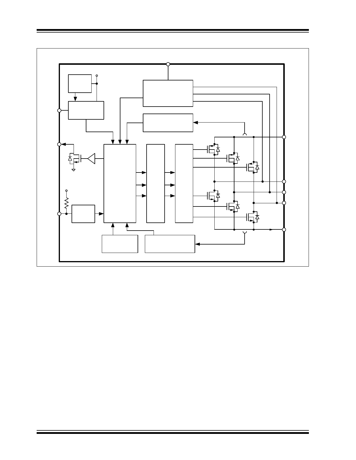
Functional Block Diagram
Thermal
protection
V
DD
OUT1
OUT2
Timing
Controller
PWM
FG
OUT3
V
CC
Short-circuit
protection
Output
Drive
Circuit
Motor Phase
Detection Circuit
Overcurrent
protection
PWM
Input
Soft
Switching
Drive
V
CC
Regulator
V
REF
GND
V
DD
BOOST
*MTD6501D Only
2010-2012 Microchip Technology Inc.
DS22263B-page 3
MTD6501C/D/G
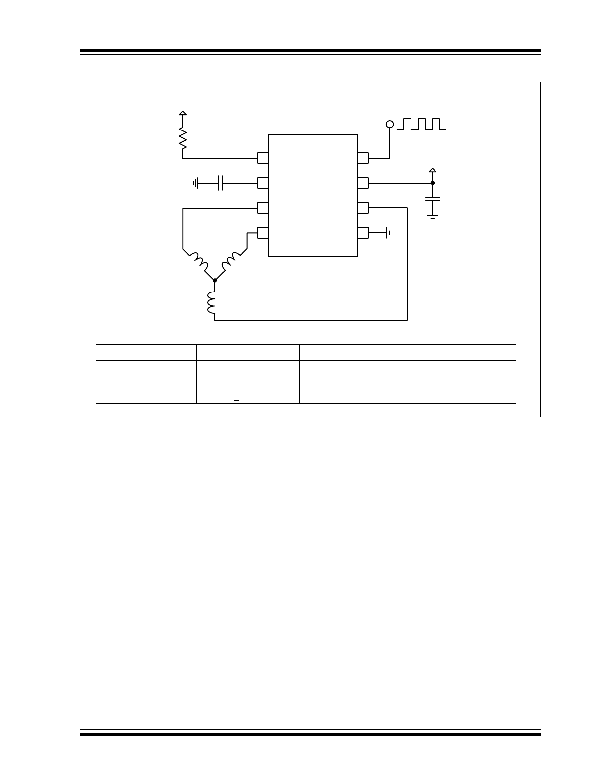
Typical Application – Fan Motor Driver Using the MTD6501C or MTD6501G
Recommended External Components for Typical Application
Element
Type/Value
Comment
C
1
>1 µF
Connect as close as possible to IC input pins
C
2
>1 µF
Connect as close as possible to IC input pins
R
1
>10 kΩ
Connect to V
logic
on controller side
OUT1
FG
V
DD
OUT2
GND
V
CC
PWM
OUT3
1
2
3
4
5
6
7
8
M
T
D6
5
0
1
C/
G
V
CC
PWM input
(0.02-100 kHz)
C
1
C
2
R
1
V
logic
(controller side)
MTD6501C/D/G
DS22263B-page 4
2010-2012 Microchip Technology Inc.
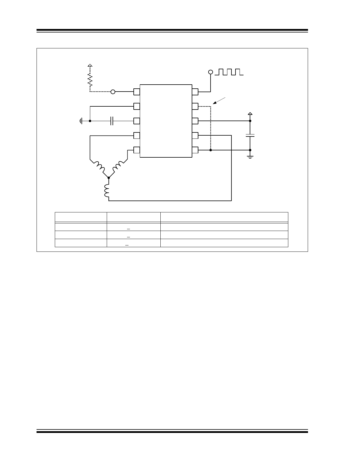
Typical Application – Fan Motor Driver Using the MTD6501D
Recommended External Components for Typical Application
Element
Type/Value
Comment
C1
>1 µF
Connect as close as possible to IC input pins
C2
>1 µF
Connect as close as possible to IC input pins
R1
>10 kΩ
Connect to Vlogic on controller side
OUT1
GND
OUT2
GND
BOOST
PWM
OUT3
1
2
4
5
6
7
9
10
M
T
D6501D
V
DD
VCC
3
8
R
1
V
logic
(controller side)
C
1
C
2
PWM input
(0.02-100 kHz)
FG
Tie to GND
for BOOST
mode
2010-2012 Microchip Technology Inc.
DS22263B-page 5
MTD6501C/D/G
1.0
ELECTRICAL
CHARACTERISTICS
Absolute Maximum Ratings†
Power Supply Voltage (V
CC_MAX
) .................... -0.7 to +15.3V
Maximum OUT1, 2, 3 Output Voltage (V
OUT_MAX
) .................
................................................................ -0.7 to +15.3V+0.7V
FG Maximum Output Voltage (V
FG_MAX
) ......... -0.7 to +15.3V
Maximum Output Current
(
3
,
4
)
(I
OUT_MAX
)....................800 mA
Maximum Output Current
(
3
,
5
)
(I
OUT_MAX
)....................500 mA
FG Maximum Output Voltage (V
FG_MAX
) ......... -0.7 to +15.3V
FG Maximum Output Current (I
FG_MAX
)
.....................5.0 mA
V
DD
Maximum Voltage (V
DD_MAX
) ..................... -0.7 to +4.0V
PWM Maximum Voltage (V
PWM_MAX
) ................ -0.7 to +4.0V
Allowable Power Dissipation
(
1
,
2
,
4
)
(P
D_MAX
).....................1.0W
Allowable Power Dissipation
(
1
,
2
,
5
)
(P
D_MAX
).....................0.5W
Max Junction Temperature (T
J
)....................................+150°C
† Notice:
Stresses above those listed under “Maximum
Ratings” may cause permanent damage to the device.
This is a stress rating only and functional operation of
the device at those or any other conditions above those
indicated in the operational listings of this specification
is not implied. Exposure to maximum rating conditions
for extended periods may affect device reliability.
Note 1:
Reference PCB, according to JEDEC
standard EIA/JESD 51-9.
2:
Derating applies for ambient temperatures
outside the specified operating range (refer
to
Figure 1-1
).
3:
OUT1, OUT2, OUT3 (Continuous,
100% duty cycle).
4:
MTD6501C and MTD6501G
5:
MTD6501D
ELECTRICAL CHARACTERISTICS
Electrical Specifications:
Unless otherwise specified, all limits are established for V
CC
= 5.0V, T
A
= +25°C
Parameters
Sym.
Min.
Typ.
Max.
Units
Conditions
Power Supply Voltage
V
CC
2
—
14
V
Power Supply Current
I
VCC
—
10
—
mA
Rotation Mode
5
Lock-Protection Mode
OUTx High Resistance
R
ON(H)
—
0.75
1
Ω
I
OUT
= 0.5A, V
CC
= 3.3V to 14V
OUTx Low Resistance
R
ON(L)
—
0.75
1
Ω
I
OUT
= -0.5A, V
CC
= 3.3V to 14V
OUTx Total Resistance
R
ON(H+L)
—
1.5
2
Ω
I
OUT
= 0.5A, V
CC
= 3.3V to 14V
V
DD
Output Voltage
V
DD
—
3
—
V
V
CC
= 3.3V to 14V
V
CC
– 0.2
V
V
CC
< 3.3V
PWM Input Frequency
f
PWM
0.02
—
100
kHz
—
PWM Input H Level
V
PWM_H
0.8*V
DD
—
3.6
V
—
PWM Input L Level
V
PWM_L
0
—
0.2*V
DD
V
—
PWM Internal Pull-Up
Current
I
PWM_L
17
34
—
µA
PWM = GND, V
CC
= 3.3V to 14V
8
17
—
µA
PWM = GND, V
CC
< 3.3V
PWM Output
Frequency
f
PWM_O
—
20
—
kHz
MTD6501C
and MTD6501D
23
kHz
MTD6501G
FG Output Pin Low
Level Voltage
V
OL_FG
—
—
0.25
V
I
FG
= -1 mA
FG Output Pin Leakage
Current
I
LH_FG
—
—
10
µA
V
FG
= 14V
Lock Protection
Operating Time
T
RUN
—
0.5
—
s
—
Lock Protection Waiting
Time
T
WAIT
4.5
5
5.5
s
—
Thermal Shutdown
T
SD
—
170
—
°C
—
Thermal Shutdown
Hysteresis
T
SD_HYS
—
25
—
°C
—
MTD6501C/D/G
DS22263B-page 6
2010-2012 Microchip Technology Inc.
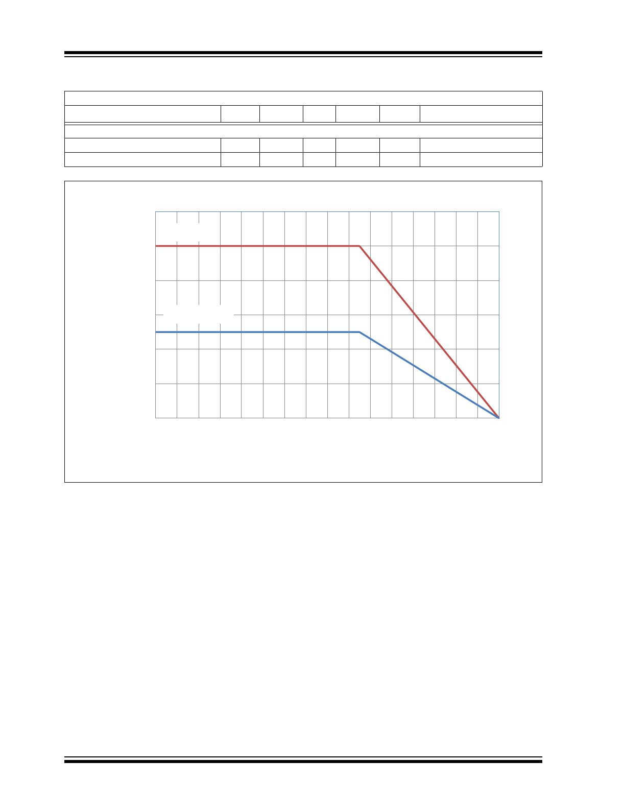
FIGURE 1-1:
Allowable Power Dissipation (P
D_MAX
) as a Function of Ambient Temperature (T
A
).
TEMPERATURE SPECIFICATIONS
Electrical Specifications:
Unless otherwise specified, all limits are established for V
CC
= 5.0V, T
A
= +25°C
Parameters
Sym.
Min.
Typ.
Max.
Units
Conditions
Temperature Ranges
Operating Temperature
T
OPR
-30
—
+95
°C
Storage Temperature Range
T
STG
-55
—
+150
°C
0
0.2
0.4
0.6
0.8
1
1.2
-10
0
10
20
30
40
50
60
70
80
90
100
11
0
120
130
140
150
P
DMA
X
(W)
T
A
(°C)
SOP-8
MSOP-10
2010-2012 Microchip Technology Inc.
DS22263B-page 7
MTD6501C/D/G
2.0
PIN DESCRIPTIONS
The descriptions of the pins are listed in
Table 2-1
.
TABLE 2-1:
MTD6501C/D/G PIN FUNCTION TABLE
MTD6501C,
MTD6501G
MTD6501D
Type
Symbol
Description
SOP-8
MSOP
1
1
O
FG
Motor speed indication output
2
3
P
V
DD
Internal regulator output (for decoupling only)
3
4
O
OUT1
Single-phase coil output pin
4
5
O
OUT2
Single-phase coil output pin
5
2, 6
P
GND
Negative voltage supply (ground)
6
7
O
OUT3
Single-phase coil output pin
7
8
P
V
CC
Positive voltage supply for motor driver
8
10
I
PWM
PWM input signal for speed control
N/A
9
I
BOOST
Boost mode selection:
• Pin floating for Normal mode
• Pin tied to GND for Boost mode
Legend:
I = Input; O = Output; P = Power

MTD6501C/D/G
DS22263B-page 8
2010-2012 Microchip Technology Inc.
NOTES:
2010-2012 Microchip Technology Inc.
DS22263B-page 9
MTD6501C/D/G
3.0
FUNCTIONAL DESCRIPTION
The MTD6501C/D/G devices generate a full-wave sig-
nal to drive a 3-phase sensorless BLDC motor. High
efficiency and low-power consumption are achieved
due to DMOS transistors and synchronous rectification
drive type. The current carrying order of the output is as
follows: OUT1
OUT2 OUT3.
3.1
Speed Control
The rotational speed of the motor can be controlled
either through the PWM digital input signal or by acting
directly on the power supply (V
CC
). When the PWM
signal is “High” (or left open) the motor rotates at full
speed. When the PWM signal is “Low”, the motor is
stopped (and the IC outputs are set to high-
impedance). By changing the PWM duty cycle, the
speed can be adjusted. Notice that the PWM frequency
has no special meaning for the motor speed and is
asynchronous with the activation of the output
transistors. Thus, the user has maximum freedom to
choose the PWM system frequency within a wide range
(from 20 Hz to 100 kHz), while the output transistor
activation always occurs at a fixed rate, which is
outside of the range of audible frequencies. The
MTD6501C and MTD6501D typical output frequency is
20 kHz. The MTD6501G output frequency is 23 kHz.
3.2
Frequency Generator Function
The Frequency Generator output is a “Hall-sensor
equivalent” digital output, giving information to an
external controller about the speed and phase of the
motor. The FG pin is an open drain output, connecting
to a logical voltage level through an external pull-up
resistor. When a lock (or out-of-sync) situation is
detected by the driver, this output is set to high-imped-
ance until the motor is restarted. Leave the pin open
when not used. The FG signal can be used to compute
the motor speed in rotations per minute (RPM). Typi-
cally, for a four pole BLDC fan, the speed in RPMs is 30
FG frequency (Hz).
3.3
Lockup Protection and Automatic
Restart
If the motor is stopped (blocked) or if it loses
synchronization with the driver, a lock-up protection
circuit detects this situation and disables the driver (by
setting its outputs to high-impedance) in order to
prevent the motor coil from burnout. After a “waiting
time” (T
WAIT
), the lock-up protection is released and
normal operation resumes for a given time (T
RUN
). In
case the motor is still blocked, a new period of waiting
time is started. T
WAIT
and T
RUN
timings are fixed
internally, so that no external capacitor is needed.
3.4
Overcurrent Protection and Short
Circuit Detection
The motor peak current is limited by the driver to a fixed
value (defined internally), thus limiting the maximum
power dissipation in the coils. The detection of a short-
circuit situation immediately sets the driver outputs to
high-impedance, in order to avoid permanent damage
to the IC.
3.5
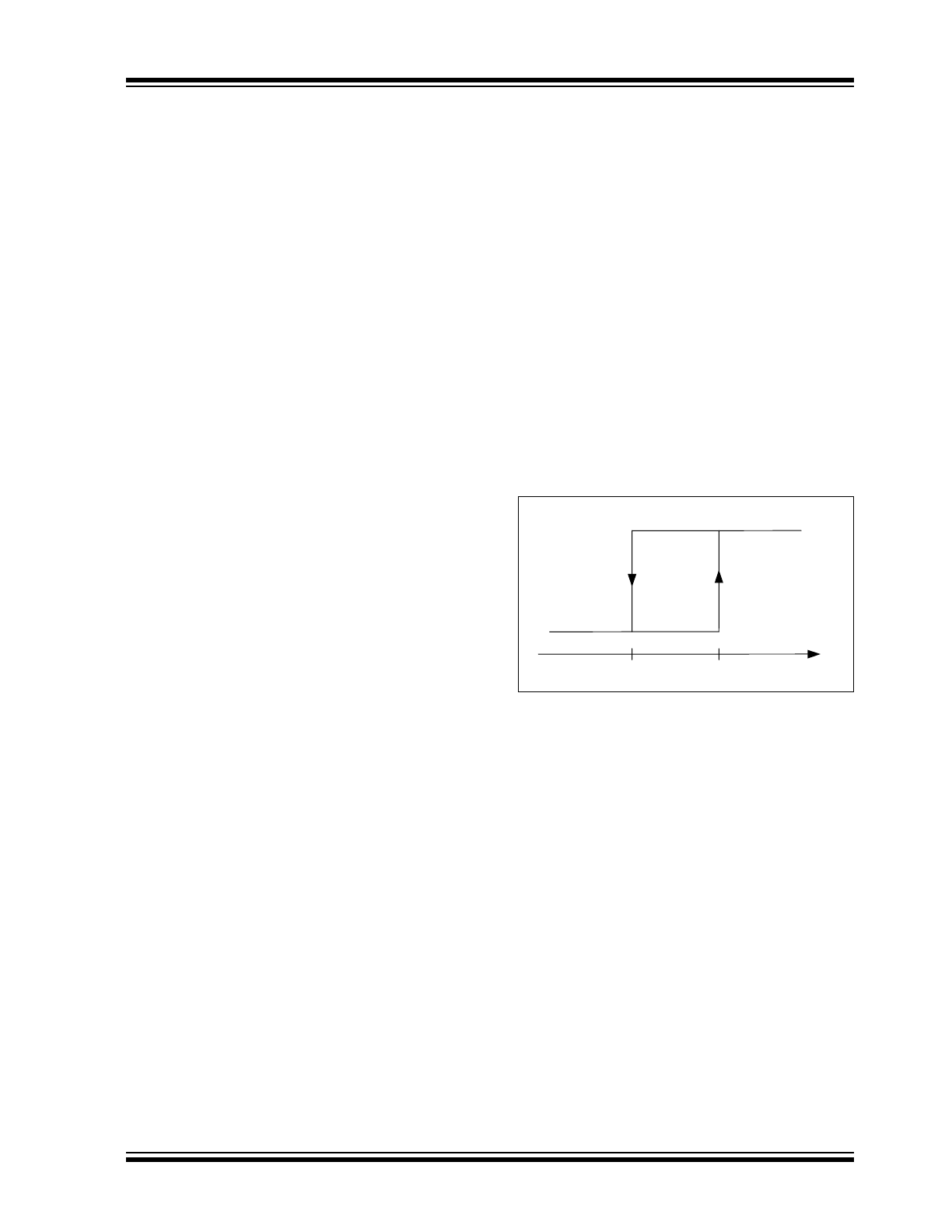
Thermal Shutdown
The MTD6501C/D/G have a thermal protection
function which detects when the die temperature
exceeds T
SD
= +170°C. When this temperature is
reached, the circuit enters Thermal Shutdown mode
and the outputs OUT1, OUT2 and OUT3 are disabled
(high-impedance), avoiding IC destruction and allowing
the circuit to cool down. Once the junction temperature
(T
SD
) has dropped below +145°C, the normal operation
resumes (thermal detection circuit has +25°C
hysteresis function).
FIGURE 3-1:
Thermal Protection
Hysteresis.
3.6
Internal Voltage Regulator
V
DD
voltage is generated internally and is used to
supply internal logical blocks. The V
DD
pin is used to
connect an external decoupling capacitor (1 µF or
higher). Notice that this pin is for IC internal use and is
not designed to supply DC current to external blocks.
T
SD
+145°C
Thermal Shutdown
+170°C
Normal operation

MTD6501C/D/G
DS22263B-page 10
2010-2012 Microchip Technology Inc.
3.7
Boost Mode (MTD6501D)
The Boost mode is an optional BEMF pre-amplification
by a factor of three. The intention of Boost mode is to
compensate for motors with a low coupling coefficient
(= BEMF coefficient), thus allowing it to cover an even
wider range of motor characteristics. Notice that Boost
mode impacts the mechanical performance of the
motor altogether. In Boost mode, the speed of the
motor will adjust faster to variations of the control (V
CC
or PWM) and/or of the load, including at start-up.
However, when the BEMF is amplified too much, the
mechanical performance (in terms of vibration and
acoustic noise) may start degrading. Thus, Boost mode
may be inappropriate for motors that already have a
good coupling coefficient. The optimum choice
between normal mode and Boost mode depends both
on the application requirements and on the motor
characteristics.
Refer to
Table 3-1
for usage of Boost pin 9; leaving this
pin floating results in the normal mode of operation,
while tying this pin to GND activates Boost mode
(active low feature, internal pull-up).
TABLE 3-1:
POSSIBLE MODES OF
OPERATION BASED ON THE
BOOST PIN CONNECTION
BOOST Pin
Mode of Operation
Floating
Normal
Tied to GND
Boost