
2012 Microchip Technology Inc.
Preliminary
DS41668A-page 1
MTCH112
Features:
• Capacitive Proximity Detection System:
- High Signal to Noise Ratio (SNR)
- Adjustable sensitivity
- Noise Rejection Filters
- Scanning method actively optimized to
attenuate strongest noise frequencies
- Automatic calibration with optional user
presets
- Dynamic threshold management adjusts
sensitivity of sensor based on the level of
environmental noise
- Constant press calibration tracks the
expected offset when the sensor is pressed
and adjusts the threshold to automatically
achieve the best press/release behavior
- User-defined “minimum shift” values specify
the lowest amount of signal change to
activate a state transition. Automatic
thresholds never decrease below these
settings.
- Automatic Environmental Compensation
- Stuck release mechanism
• No Required External Components
• Low-Power mode: Highly Configurable
Low-Power mode
- 1 ms to 4s Sleep interval between sensor
samples
• Response Time as Low as 10 ms
• Hardware Error Detection notifies if either sensor
is shorted to V
DD
, V
SS
or the other sensor
• Operating Voltage Range:
- 1.8V to 3.3V
• Operating Temperature:
- 40°C to +85°C
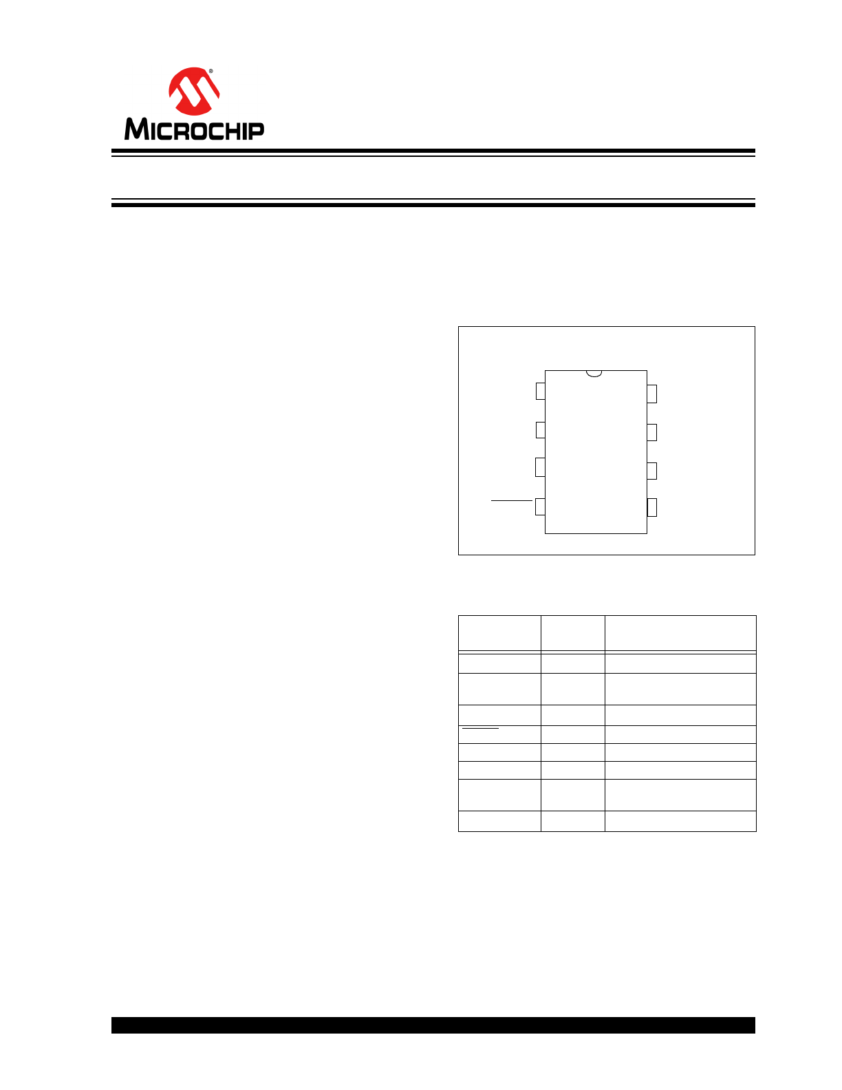
Package Type
The device is available in 8-lead SOIC and DFN
packaging (see
Figure 1
).
FIGURE 1:
8-PIN DIAGRAM
FOR
MTCH112
TABLE 1:
8-PIN SOIC/DFN PINOUT
DESCRIPTION
I/O
8-Pin
SOIC/DFN
Description
V
DD
1
Power Supply Input
MTO/INT
2
Detect Output (Active-Low)
Notification Interrupt Pin
MTI0
3
Proximity/Touch Sensor Input
RESET
4
Device Reset (Active-Low)
SDA
5
I
2
C™ Data
SCL
6
I
2
C™ Clock
MTI1/MTGRD0
7
Proximity/Touch Sensor Input
Active Guard Shield for MTI0
V
SS
8
Ground Reference
MTI0
RESET
V
DD
MTO/INT
V
SS
MTI1/MTGRD0
SDA
SCL
1
2
3
4
5
6
8
SOIC, DFN
7
MTCH1
1
2
Dual-Channel Proximity/Touch Controller

MTCH112
DS41668A-page 2
Preliminary
2012 Microchip Technology Inc.
Table of Contents
1.0
Device Overview ........................................................................................................................................................................ 3
2.0
I
2
C™ Serial Interface ................................................................................................................................................................. 6
3.0
Configuration Registers ........................................................................................................................................................... 13
4.0
Electrical Characteristics.......................................................................................................................................................... 25
5.0
Packaging Information ............................................................................................................................................................. 34
Index ........................................................................................................... ........................................................................................ 42
The Microchip Web Site ....................................................................................................................................................................... 43
Customer Change Notification Service ................................................................................................................................................ 43
Customer Support ................................................................................................................................................................................ 43
Reader Response ................................................................................................................................................................................ 44
Product Identification System .............................................................................................................................................................. 45
TO OUR VALUED CUSTOMERS
It is our intention to provide our valued customers with the best documentation possible to ensure successful use of your Microchip
products. To this end, we will continue to improve our publications to better suit your needs. Our publications will be refined and
enhanced as new volumes and updates are introduced.
If you have any questions or comments regarding this publication, please contact the Marketing Communications Department via
E-mail at
docerrors@microchip.com
or fax the Reader Response Form in the back of this data sheet to (480) 792-4150. We
welcome your feedback.
Most Current Data Sheet
To obtain the most up-to-date version of this data sheet, please register at our Worldwide Web site at:
http://www.microchip.com
You can determine the version of a data sheet by examining its literature number found on the bottom outside corner of any page.
The last character of the literature number is the version number, (e.g., DS30000A is version A of document DS30000).
Errata
An errata sheet, describing minor operational differences from the data sheet and recommended workarounds, may exist for current
devices. As device/documentation issues become known to us, we will publish an errata sheet. The errata will specify the revision
of silicon and revision of document to which it applies.
To determine if an errata sheet exists for a particular device, please check with one of the following:
• Microchip’s Worldwide Web site;
http://www.microchip.com
• Your local Microchip sales office (see last page)
When contacting a sales office, please specify which device, revision of silicon and data sheet (include literature number) you are
using.
Customer Notification System
Register on our web site at
www.microchip.com
to receive the most current information on all of our products.

2012 Microchip Technology Inc.
Preliminary
DS41668A-page 3
MTCH112
1.0
DEVICE OVERVIEW
The Microchip mTouch™ sensing MTCH112 Dual-
Channel Proximity/Touch Controller provides an easy
way to add proximity and/or touch sensor detection to
any application. The device implements either two
capacitive sensors or one sensor and one active guard
driver. The optional device configuration through I
2
C™
allows presets to be loaded in a production environ-
ment. Automatic calibration routines are used by
default to choose the best options, so user configura-
tion is not required.
The MTCH112 uses a sophisticated optimization
algorithm to actively eliminate noise from the signal.
While the noise level is being measured, the
requirements for a proximity or touch detection are
updated to reflect the degree of uncertainty in the
readings. When a press is detected for the first time,
the threshold is automatically calibrated to choose a
smart threshold for the ‘release’ and next press. This
creates a system that dynamically optimizes the signal-
to-noise ratio for its environment.
1.1
Automatic Calibration
It measures the amount of capacitance on each sensor
pin and chooses the best of three possible waveforms
to capture a capacitive measurement.
It analyzes the two final settling voltages of the MTI0
pin to more closely match the waveform on the
MTGRD0 pin.
The settling time for the waveform is calibrated to
maximize sensitivity while minimizing the delay. This
provides the best trade-off between signal and noise
reduction.
Calibration results are stored in the on-board EEPROM
for faster recovery time on next power-up. These
memory locations are accessible for read/write through
the I
2
C communications to bypass the automatic
calibration, if required.
1.2
Communications
• I
2
C, Slave mode
1.3
Touch Configurations
• MTI0 is a dedicated capacitive sensor input
• MTI1/MTGRD0 can either be another capacitive
sensor or a guard driver for MTI0
1.4
Signal Resolution
• 13 bits
1.5
Pin Description
1.5.1
MTI0/MTI1
Connect the sensor to this input. An additional resistor
of at least 4.7 k
is recommended for best noise
immunity. Sensors up to 40 pF in capacitance are
supported. Sensors work best when the base
capacitance is minimized. This will maximize the
percentage change in capacitance when a finger is
added to the circuit.
1.5.2
MTGRD0
When not scanning the pin for capacitance changes
(MTI1 functionality), the pin will be driven in phase with
MTI0 to minimize the voltage differential between the
two pins. If the MTGRD0 pin’s trace surrounds the
MTI0 pin’s trace, the waveform on MTGRD0 will shield
(or guard) MTI0 from the effect of nearby noise sources
or power planes.
1.5.3
MTO
The mTouch™ sensing
output pin is always driven to
either V
DD
or V
SS
by the device. The MTCH112
OUTCON register (see
Register 3-1
) determines the
behavior of the MTO/INT pin. The pin is always active-
low, but the states in which this output occurs can be
adjusted in the device’s OUTCON register. If no options
are selected for output states, the MTO pin acts as an
interrupt to a master device. The MTCH112 will pulse
low for at least 1 ms if any state changes occur. Further
information must be determined by communicating
through I
2
C with the device.
1.5.4
I
2
C – SERIAL DATA PIN (SDA)
The SDA pin is the serial data pin of the I
2
C interface.
The SDA pin is used to write or read the registers and
Configuration bits. The SDA pin is an open-drain
N-channel driver. Therefore, it needs an external pull-
up resistor from the V
DD
line to the SDA pin. The rec-
ommended resistance value is 1.5 k
. Except for Start
and Stop conditions, the data on the SDA pin must be
stable during the high period of the clock. The high or
low state of the SDA pin can only change when the
clock signal on the SCL pin is low. Refer to
Section 2.1.2 “I2C Operation”
for more details on I
2
C
Serial Interface communication.
MTCH112
DS41668A-page 4
Preliminary
2012 Microchip Technology Inc.
1.5.5
I
2
C – SERIAL CLOCK PIN (SCL)
The SCL pin is the serial clock pin of the I
2
C interface.
The I
2
C interface only acts as a slave and the SCL pin
accepts only external serial clocks. The input data from
the master device is shifted into the SDA pin on the
rising edges of the SCL clock, and output from the
device occurs at the falling edges of the SCL clock. The
SCL pin is an open-drain N-channel driver. Therefore,
it needs an external pull-up resistor from the V
DD
line to
the SCL pin. The recommended resistance value is
1.5 k
. Refer to
Section 2.1.2 “I2C Operation”
for
more details on I
2
C Serial Interface communication.
For more details, see
Figure 1
and
Table 1
.
1.6
Performance
1.6.1
PROXIMITY DISTANCE
The maximum proximity distance will be highly
dependent on the level of noise in the environment. To
maximize the robustness of the controller, the noise
level is measured and used to define how much shift is
required in the signal before a reliable change in state
can be determined. These values were taken in a low-
noise environment. For more details, see
Figure 4-2
.
1.6.2
RESPONSE TIME
The response time is defined as the maximum amount
of time delay between the sensor’s capacitance signif-
icantly changing and the output being updated based
on the OUTCON register’s configuration.
This amount of time will be dependent on the LPCON
register, as it determines how long the device will sleep
after detecting no significant changes. The fastest
response time can be achieved by setting the LPCON
register for the minimum Sleep time (see
Register 3-6
).
The controller only sleeps when idle and no changes in
the environment are detected. If a change occurs, the
device will operate without sleeping until the
disturbance or capacitance is removed. For more
details, see
Table 4-2
.
1.6.3
HARDWARE
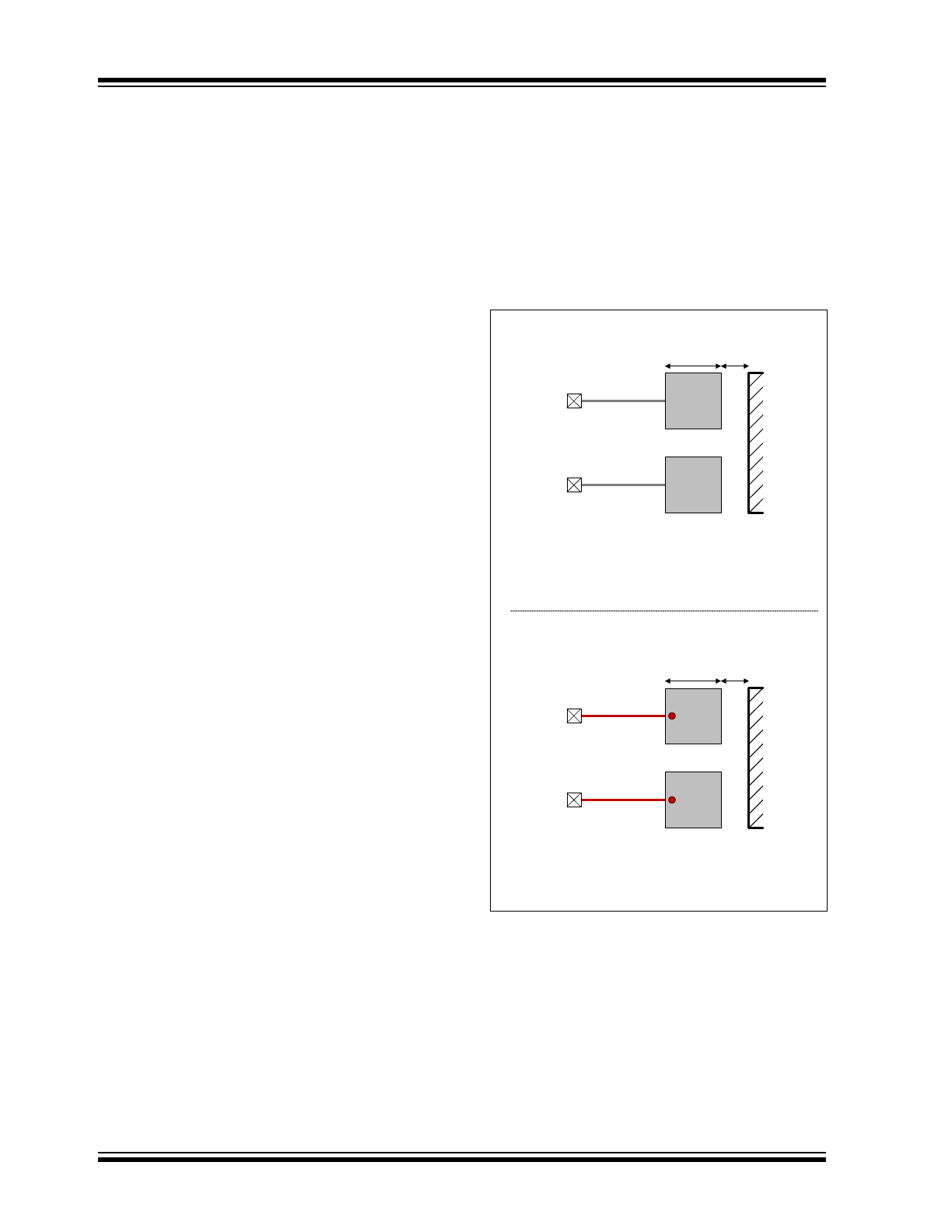
Capacitive sensors are areas of metal connected
through a series resistor of 4.7 kΩ to one of the MTIx
pins. The following diagrams show some example
layout configurations along with the recommended
design guidelines. For more information about the
design of capacitive sensors, see AN1334,
“Techniques for Robust Touch Sensing Design”.
FIGURE 1-1:
TWO-SENSOR LAYOUTS
— EXAMPLE
G
rou
n
d P
lan
e
or
Noi
se Sou
rc
e
MTIN1
MTIN0
(1)
(2)
NOTE:
1: 15 mm x 15 mm recommended.
2: Maximize separation distance.
3: Thickness of traces to pin: 0.1 – 0.5 mm
Single Layer PCB, Two Sensors
(3)
Gr
ou
nd P
la
n
e o
r
Noi
se
So
ur
ce
MTIN1
MTIN0
(1)
(2)
NOTE:
1: 15 mm x 15 mm recommended.
2: Maximize separation distance.
3: Thickness of traces to pin: 0.1 – 0.5 mm
Two Layer PCB, Two Sensors
(3)
2012 Microchip Technology Inc.
Preliminary
DS41668A-page 5
MTCH112
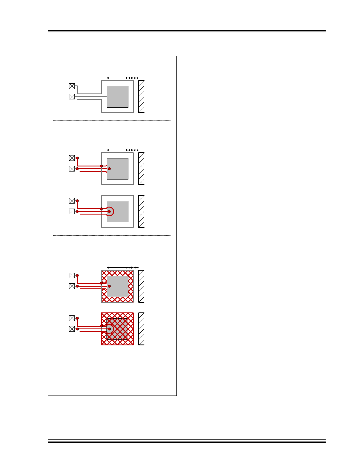
FIGURE 1-2:
GUARD LAYOUTS —
EXAMPLE
(1)
(2) (3)
Front View
Back View
(1)
(2) (3)
Front View
Back View
Gr
ou
nd P
lane
o
r
A
dj
ac
ent
S
en
sor
Layout for Thin PCBs
Layout for Reverse-side Shielding
(Min. PCB layer separation of 1.5mm is recommended.)
Gr
ou
nd P
lane
o
r
A
dj
ac
ent
S
en
sor
Ground
P
lan
e
or
Ad
ja
ce
n
t Se
ns
or
(1)
(2) (3)
Layout for Single Layer PCBs
NOTE:
1: 15 mm x 15 mm recommended.
2: >2 mm separation recommended.
3: >2 mm separation recommended.
4: Thickness of traces to pin: 0.1 – 0.5 mm
>0.5 mm separation recommended.
5: Thickness of guard around sensor: 1 mm
MTGRD0
MTIN0
MTGRD0
MTIN0
MTGRD0
MTIN0
MTGRD0
MTIN0
MTGRD0
MTIN0
(4)
(4)
(4)
MTCH112
DS41668A-page 6
Preliminary
2012 Microchip Technology Inc.
2.0
I
2
C™ SERIAL INTERFACE
This device supports the I
2
C serial protocol. The I
2
C
module operates in Slave mode, so it does not
generate the serial clock.
2.1
Overview
This I
2
C interface is a two-wire interface.
Figure 2-1
shows a typical I
2
C Interface connection.
The I
2
C interface specifies different communication bit
rates. These are referred to as Standard, Fast or High
Speed modes. The MTCH112 device supports these
three modes. The bit rates of these modes are:
• Standard Mode: Bit Rates up to 100 kbit/s
• Fast Mode: Bit Rates up to 400 kbit/s
A device that sends data onto the bus is defined as a
transmitter, and a device receiving data is defined as a
receiver. The bus has to be controlled by a master
device which generates the serial clock (SCL), controls
the bus access and generates the Start and Stop
conditions. The MTCH112 device works as slave. Both
master and slave can operate as transmitter or
receiver, but the master device determines which mode
is activated. Communication is initiated by the master
(microcontroller) which sends the Start bit, followed by
the slave address byte. The first byte transmitted is
always the slave address byte, which contains the
device code, the address bits and the R/W bit.
FIGURE 2-1:
TYPICAL I
2
C™
INTERFACE
The I
2
C serial protocol only defines the field types, field
lengths, timings, etc. of a frame. The frame content
defines the behavior of the device. For details on the
frame content (commands/data) refer to
Section 2.3
“I2C Commands”
.
Refer to the NXP User Manual (UM10204_3) for more
details on the I
2
C specifications.
There was some concern as to the use of the
Acknowledge bit to indicate a command error
condition. From Section 3.6 of the NXP User Manual
(UM10204_3, Rev 03 - 19 June 2007), the description
states:
“
The acknowledge takes place after every byte. The
Acknowledge bit allows the receiver to signal the
transmitter that the byte was successfully received and
another byte may be sent. All clock pulses including the
acknowledge 9th clock pulse are generated by the
master.
”
From this we can state that the byte was not “
success-
fully received
” since it is an invalid combination of
Address/Command.
2.1.1
SIGNAL DESCRIPTIONS
The I
2
C interface uses up to two pins (signals). These
are:
• SDA (Serial Data) (see
Section 1.5.4 “I2C –
Serial Data Pin (SDA)”
)
• SCL (Serial Clock) (see
Section 1.5.5 “I2C –
Serial Clock Pin (SCL)”
)
2.1.2
I
2
C OPERATION
The MTCH112 device I
2
C module is compatible with
the NXP I
2
C specification. The following lists some of
the module’s features:
• 7-bit Slave Addressing
• Supports Two Clock Rate modes:
- Standard mode, clock rates up to 100 kHz
- Fast mode, clock rates up to 400 kHz
• Support Multi-Master Applications
The I
2
C 10-bit addressing mode is not supported.
The NXP I
2
C specification only defines the field types,
field lengths, timings, etc. of a frame. The frame
content defines the behavior of the device. The frame
content for this device is defined in
Section 2.3 “I2C
Commands”
.
I
2
C BIT STATES AND SEQUENCE
Figure 2-7
shows an I
2
C 8-bit transfer sequence, while
Figure 2-8
shows the bit definitions. The serial clock is
generated by the master. The following definitions are
used for the bit states:
• Start bit (S)
• Data bit
• Acknowledge (A) bit (driven low) /
No Acknowledge (A) bit (not driven low)
• Repeated Start bit (Sr)
• Stop bit (P)
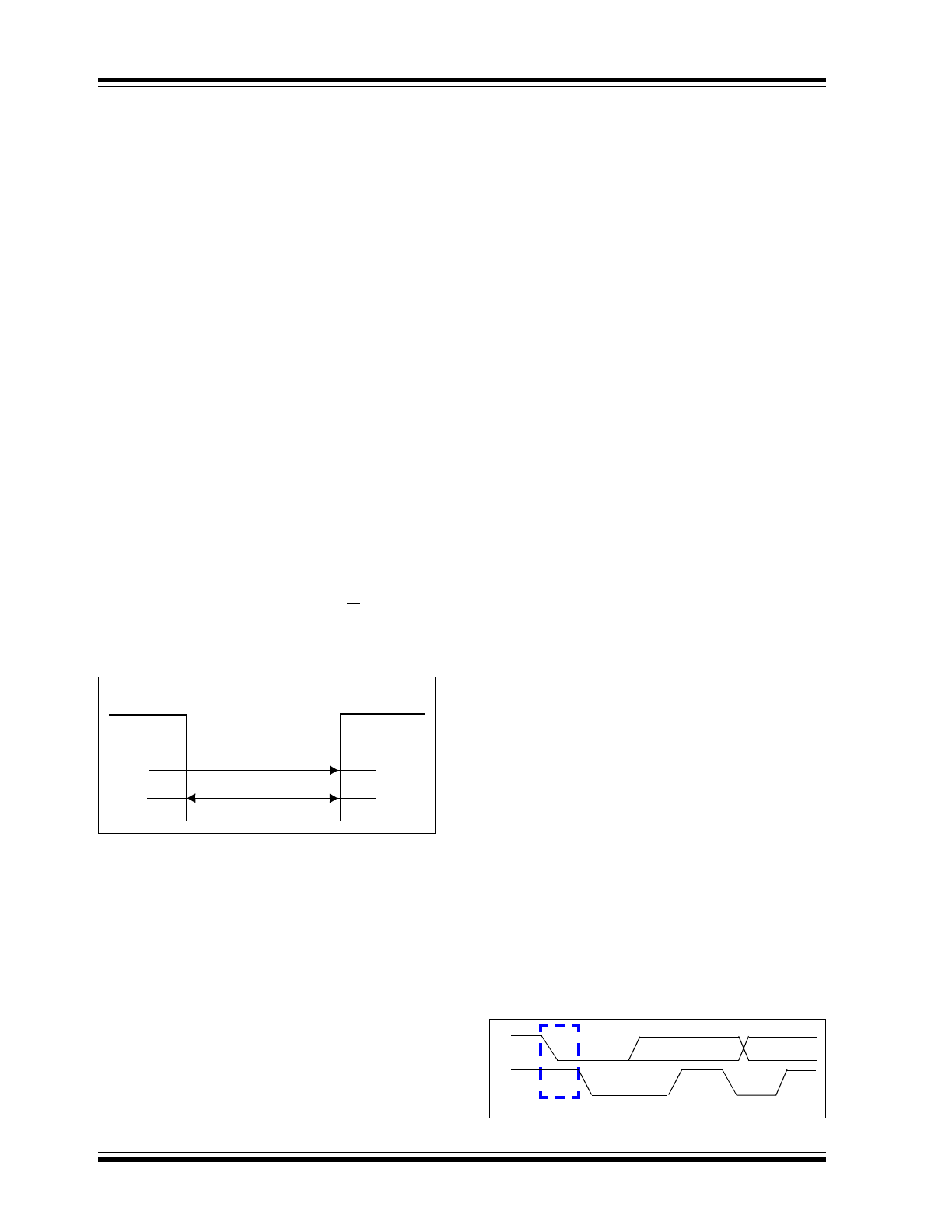
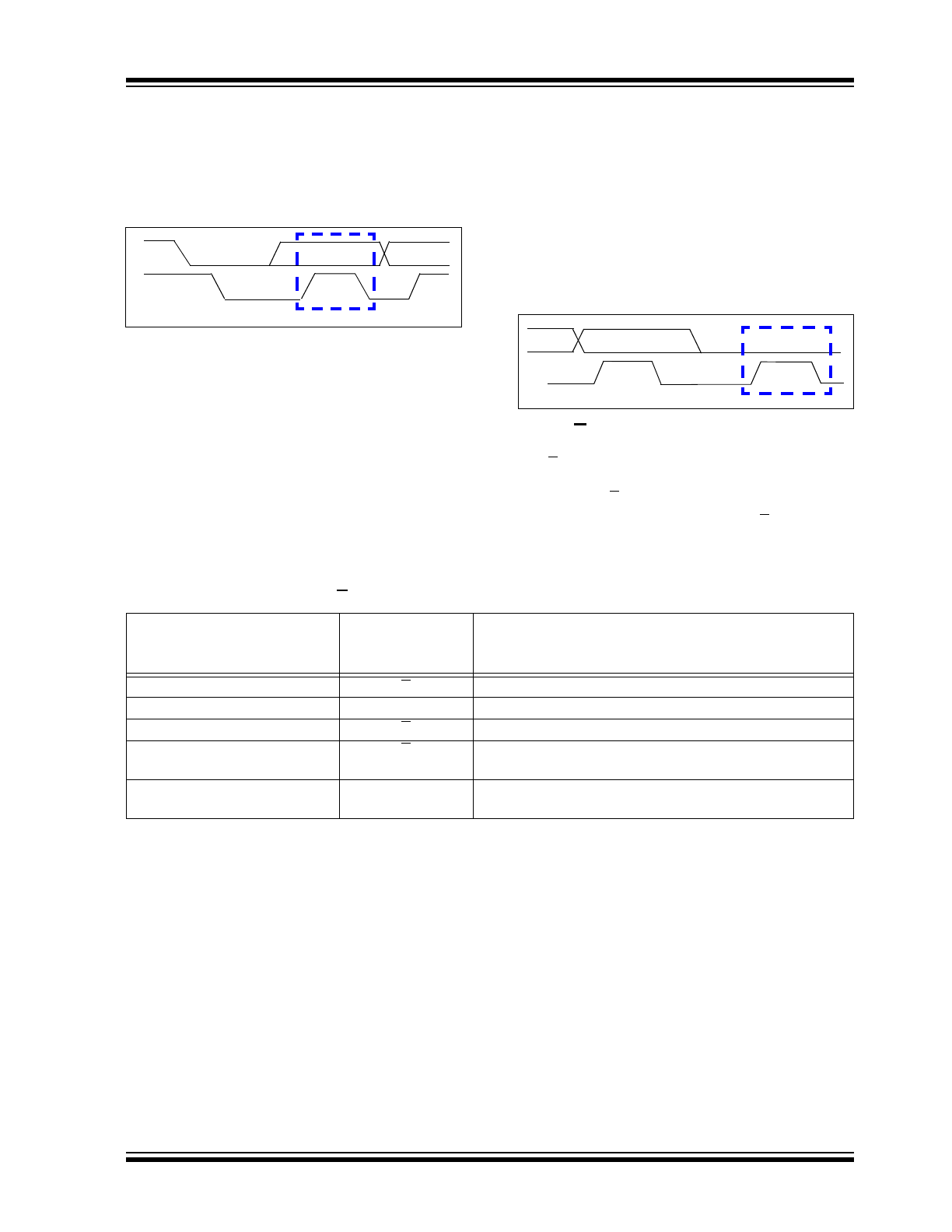
START BIT
The Start bit (see
Figure 2-2
) indicates the beginning of
a data transfer sequence. The Start bit is defined as the
SDA signal falling when the SCL signal is high.
FIGURE 2-2:
START BIT
SCL
SCL
MTCH112
SDA
SDA
Host
Controller
Typical I
2
C™ Interface Connections
SDA
SCL
S
1st Bit
2nd Bit
2012 Microchip Technology Inc.
Preliminary
DS41668A-page 7
MTCH112
DATA BIT
The SDA signal may change state while the SCL signal
is low. While the SCL signal is high, the SDA signal
MUST be stable (see
Figure 2-3
).
FIGURE 2-3:
DATA BIT
ACKNOWLEDGE (A) BIT
The A bit (see
Figure 2-4
) is typically a response from
the receiving device to the transmitting device.
Depending on the context of the transfer sequence, the
A bit may indicate different things. Typically, the slave
device will supply an A response after the Start bit and
8 data bits have been received. An A bit has the SDA
signal low.
FIGURE 2-4:
ACKNOWLEDGE
WAVEFORM
Not A (A) Response
The A bit has the SDA signal high.
Table 2-1
shows
some of the conditions where the slave device will
issue a Not A (A).
If an error condition occurs (such as an A instead of A),
then a Start bit must be issued to reset the command
state machine.
SDA
SCL
Data Bit
1st Bit
2nd Bit
A
8
D0
9
SDA
SCL
TABLE 2-1:
MTCH112 A / A RESPONSES
Event
Acknowledge
Bit
Response
Comment
General Call
A
Slave Address valid
A
Slave Address not valid
A
Communication during EEPROM
Write cycle
A
The device will NACK after a valid write sequence until all
bytes are executed.
Bus Collision
N/A
Treated as “Don’t Care” if the collision occurs on the Start
bit. Otherwise, I
2
C™ resets.
MTCH112
DS41668A-page 8
Preliminary
2012 Microchip Technology Inc.
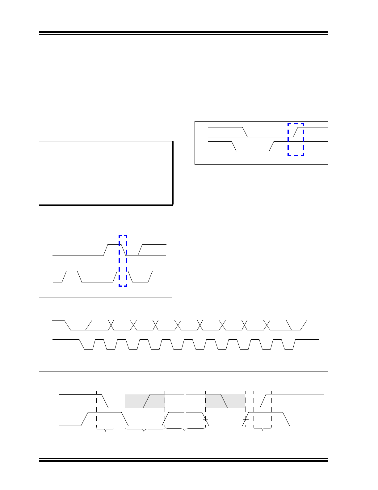
REPEATED START BIT
The Repeated Start bit (see
Figure 2-5
) indicates that
the current master device wishes to continue commu-
nicating with the current slave device without releasing
the I
2
C bus. The Repeated Start condition is the same
as the Start condition, except that the Repeated Start
bit follows a Start bit (with the data bits + A bit) and not
a Stop bit.
The Start bit is the beginning of a data transfer
sequence and is defined as the SDA signal falling when
the SCL signal is high.
FIGURE 2-5:
REPEAT START
CONDITION WAVEFORM
STOP BIT
The Stop bit (see
Figure 2-6
) indicates the end of the
I
2
C data transfer sequence. The Stop bit is defined as
the SDA signal rising when the SCL signal is high.
A Stop bit resets the I
2
C interface of the MTCH112
device.
FIGURE 2-6:
STOP CONDITION
RECEIVE OR TRANSMIT
MODE
2.1.2.1
Clock Stretching
Clock stretching is something that the receiving device
can do to allow additional time to respond to the data
that has been received.
This device will stretch the clock signal (SCL) after a
Write command to allow the EEPROM write operation
to complete.
2.1.2.2
Aborting a Transmission
If any part of the I
2
C transmission does not meet the
command format, it is aborted. This can be intentionally
accomplished with a Start or Stop condition. This is
done so that noisy transmissions (usually an extra Start
or Stop condition) are aborted before they corrupt the
device.
FIGURE 2-7:
TYPICAL 8-BIT I
2
C™ WAVEFORM FORMAT
FIGURE 2-8:
I
2
C™ DATA STATES AND BIT SEQUENCE
Note 1: A bus collision during the Repeated Start
condition occurs if:
• SDA is sampled low when SCL goes
from low-to-high.
• SCL goes low before SDA is
asserted low. This may indicate that
another master is attempting to
transmit a data “1”.
SDA
SCL
Sr = Repeated Start
1st Bit
SCL
SDA A / A
P
1st Bit
SDA
SCL
S
2nd Bit 3rd Bit
4th Bit 5th Bit 6th Bit
7th Bit
8th Bit
P
A / A
SCL
SDA
Start
Condition
Stop
Condition
Data allowed
to change
Data or
A valid
2012 Microchip Technology Inc.
Preliminary
DS41668A-page 9
MTCH112
2.1.2.3
Slope Control
This device does not implement slope control on the
SDA output.
2.1.2.4
Device Addressing
The address byte is the first byte received following the
Start condition from the master device. The full 7 bits of
the I
2
C slave address is user programmable. The
default address is “1110011”.
Figure 2-9
shows the I
2
C slave address byte format,
which contains the seven address bits and a Read/
Write (R/W) bit.
FIGURE 2-9:
SLAVE ADDRESS BITS IN
THE I
2
C™ CONTROL
BYTE
Start bit
Read/Write bit
Address Byte
R/W ACK
Acknowledge bit
Slave Address
A6
A5
A4
A3
Slave Address (7 bits)
A2
A1
A0
Note 1: Address Bits (A6:A0) can be reprogrammed
by the customer.
1
1
1
0
0
1
1
A0 Address
Note 1
MTCH112
DS41668A-page 10
Preliminary
2012 Microchip Technology Inc.
2.2
Device Commands
This section documents the commands that the device
supports.
The commands can be grouped into the following
categories:
• Write Memory
• Read Memory
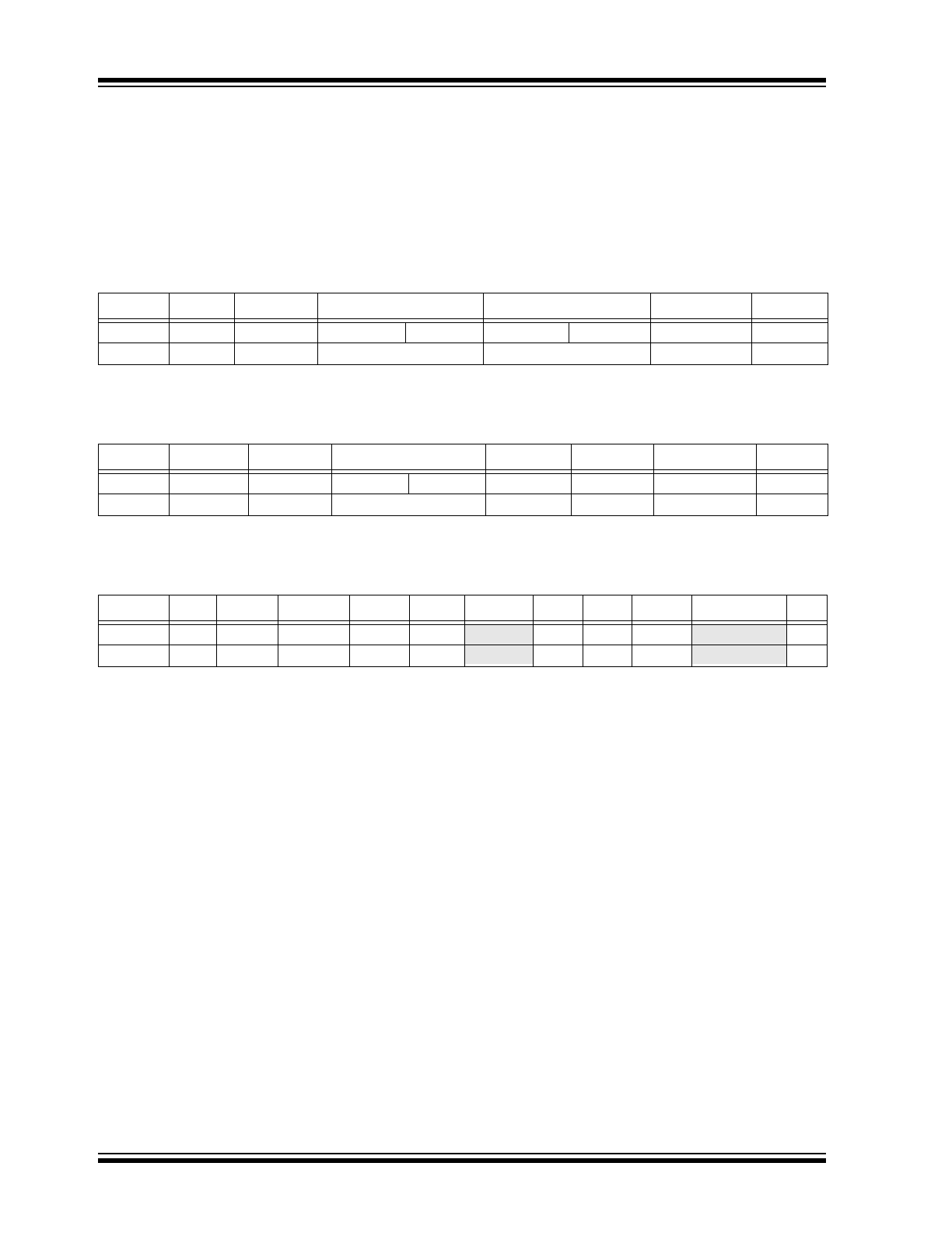
TABLE 2-2:
RESET TO FACTORY SETTINGS
Desc.
Start
Device
Write Protection
Reset Command
Checksum
(1)
Stop
Example
S
0xE6
0x55
0xAA
0x00
0xFF
0x00
P
Notes
—
Write
Required
Factory Settings
—
—
Note 1:
Checksum is the binary XOR of all bytes except the device address.
TABLE 2-3:
WRITE TO REGISTER
Desc.
Start
Device
Write Protection
Register
Value
Checksum
(1)
Stop
Example
S
0xE6
0x55
0xAA
0x01
0x01
0xFF
P
Notes
—
Write
Required
OUTCON
—
—
—
Note 1:
Checksum is the binary XOR of all bytes except the device address.
TABLE 2-4:
READ FROM REGISTER
Desc.
Start
Device
Register Restart Device
Data
Stop
Start
Device Checksum
(1)
Stop
Example
S
0xE6
0x80
S
0xE7
—
P
S
0xE7
0xZZ
P
Notes
Write
STATE
Read
—
Read
—
Note 1:
Read checksum is the binary XOR of all bytes in the Data column. This is an optional step. The checksum
can be ignored if the master does not wish to read it.