
2011-2012 Microchip Technology Inc.
Preliminary
DS75017B-page 1
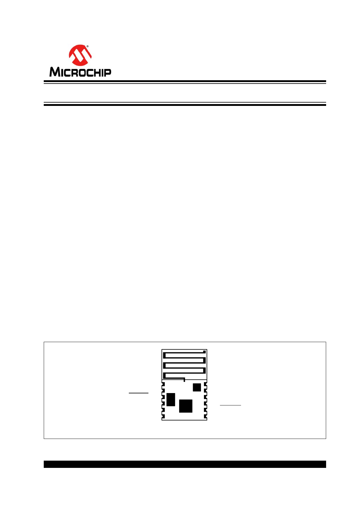
MRF89XAM9A
Features
• Module designed from the MRF89XA Integrated
Ultra Low-Power, Sub-GHz Transceiver IC
• Supports MiWi™ Development Environment
Proprietary Wireless Networking Protocols
• 4-Wire Serial Peripheral Interface (SPI) with
Interrupts
• Small Size: 0.7" x 1.1" (17.8 mm x 27.9 mm),
Surface Mountable – pin compatible with
MRF89XAM8A
• Integrated Crystal, Internal Voltage Regulator,
Matching Circuitry and Printed Circuit Board
(PCB) Antenna
• Easy Integration into Final Product – Minimize
Product Development, Quicker Time to Market
• Compatible with Microchip’s Microcontroller
Families (PIC16, PIC18, PIC24, dsPIC33 and
PIC32)
• Modular Device Approval for United States (FCC),
Canada (IC) and Radio Regulation Certified for
Australia/New Zealand (C-TICK)
Operational
• Operating Voltage: 2.1–3.6V (3.3V typical)
• Temperature Range: -40°C to +85°C Industrial
• Low-Current Consumption:
- Rx mode: 3 mA (typical)
- Tx mode: 25 mA at +10 dBm (typical)
- Sleep: 0.1 µA (typical)
RF/Analog Features
• ISM Band 902–928 MHz Operation
• Modulation: FSK and OOK
• Data Rate:
- FSK: 200 kbps
- OOK: 28 kbps
• Reception sensitivity
- FSK: -105 dBm (typical) at 25 kbps
- OOK: -111 dBm (typical) at 2 kbps
• +10 dBm Typical Output Power with 21 dB Tx
Power Control Range
Media Access Controller (MAC)/
Baseband Features
• Packet handling feature with data whitening and
automatic CRC generation
• Incoming sync word (pattern) recognition
• Built-in bit synchronizer for incoming data, and clock
synchronization and recovery
• 64-byte transmit/receive FIFO with preload in Stand-by
mode
• Supports Manchester encoding/decoding
techniques
Pin diagram
2
3
4
5
6
1
7
V
IN
GND
8
9
10
RESET
CSCON
SDO
SDI
SCK
CSDATA
IRQ1
GND
IRQ0
12
11 GND
915 MHz Ultra Low-Power Sub-GHz Transceiver Module

MRF89XAM9A
DS75017B-page 2
Preliminary
2011-2012 Microchip Technology Inc.
Table of Contents
1.0
Device Overview .......................................................................................................................................................................... 3
2.0
Circuit Description ........................................................................................................................................................................ 9
3.0
Regulatory Approval................................................................................................................................................................... 17
4.0
Electrical Characteristics ............................................................................................................................................................ 23
Appendix A: Revision History............................................................................................................................................................... 29
The Microchip Web Site ....................................................................................................................................................................... 31
Customer Change Notification Service ................................................................................................................................................ 31
Customer Support ................................................................................................................................................................................ 31
Reader Response ................................................................................................................................................................................ 32
Product Identification System............................................................................................................................................................... 33
TO OUR VALUED CUSTOMERS
It is our intention to provide our valued customers with the best documentation possible to ensure successful use of your Microchip
products. To this end, we will continue to improve our publications to better suit your needs. Our publications will be refined and
enhanced as new volumes and updates are introduced.
If you have any questions or comments regarding this publication, please contact the Marketing Communications Department via
E-mail at docerrors@microchip.com or fax the Reader Response Form in the back of this data sheet to (480) 792-4150. We
welcome your feedback.
Most Current Data Sheet
To obtain the most up-to-date version of this data sheet, please register at our Worldwide Web site at:
http://www.microchip.com
You can determine the version of a data sheet by examining its literature number found on the bottom outside corner of any page.
The last character of the literature number is the version number, (e.g., DS30000A is version A of document DS30000).
Errata
An errata sheet, describing minor operational differences from the data sheet and recommended workarounds, may exist for current
devices. As device/documentation issues become known to us, we will publish an errata sheet. The errata will specify the revision
of silicon and revision of document to which it applies.
To determine if an errata sheet exists for a particular device, please check with one of the following:
• Microchip’s Worldwide Web site; http://www.microchip.com
• Your local Microchip sales office (see last page)
When contacting a sales office, please specify which device, revision of silicon and data sheet (include literature number) you are
using.
Customer Notification System
Register on our web site at www.microchip.com to receive the most current information on all of our products.
2011-2012 Microchip Technology Inc.
Preliminary
DS75017B-page 3
MRF89XAM9A
1.0
DEVICE OVERVIEW
The MRF89XAM9A is an ultra low-power sub-GHz
surface mount transceiver module with integrated
crystal, internal voltage regulator, matching circuitry
and PCB antenna. The MRF89XAM9A module
operates in the United States/Canada 902–928 MHz
ISM frequency band. The integrated module design
frees the integrator from extensive RF and antenna
design, and regulatory compliance testing, ballowing
quicker time to market.
The MRF89XAM9A module is compatible with
Microchip’s MiWi™ Development Environment software
stacks. The software stacks are available as a free
download, including source code, from the Microchip’s
web site
http://www.microchip.com/wireless
.
The MRF89XAM9A module has received regulatory
approvals for modular devices in the United States
(FCC) and Canada (IC). Modular device approval
removes the need for expensive RF and antenna
design, and allows the user to place the MRF89XAM9A
module inside a finished product and it does not require
regulatory testing for an intentional radiator (RF
transmitter). To maintain conformance, refer to module
settings in
Section 3.1.1, MRF89XAM9A SETTINGS
for the United States and
Section 3.2.1, MRF89XAM9A
SETTINGS
for Canada.
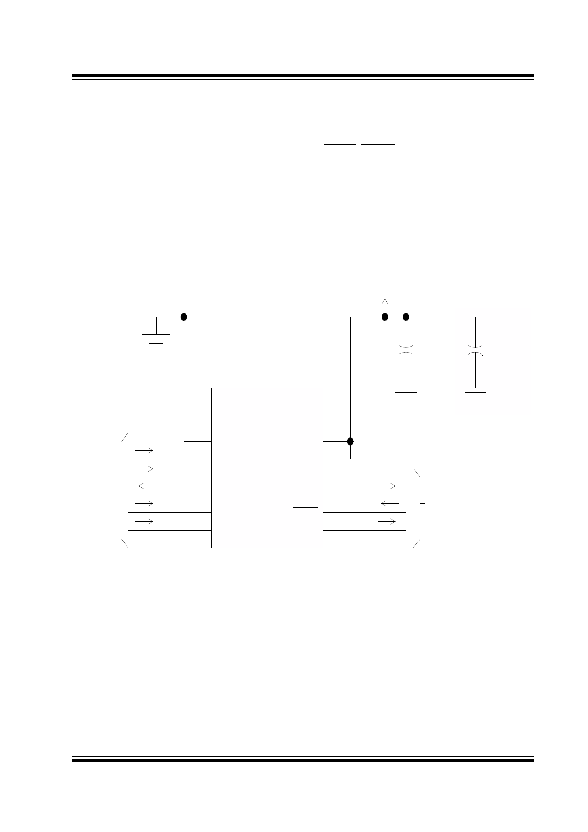
1.1
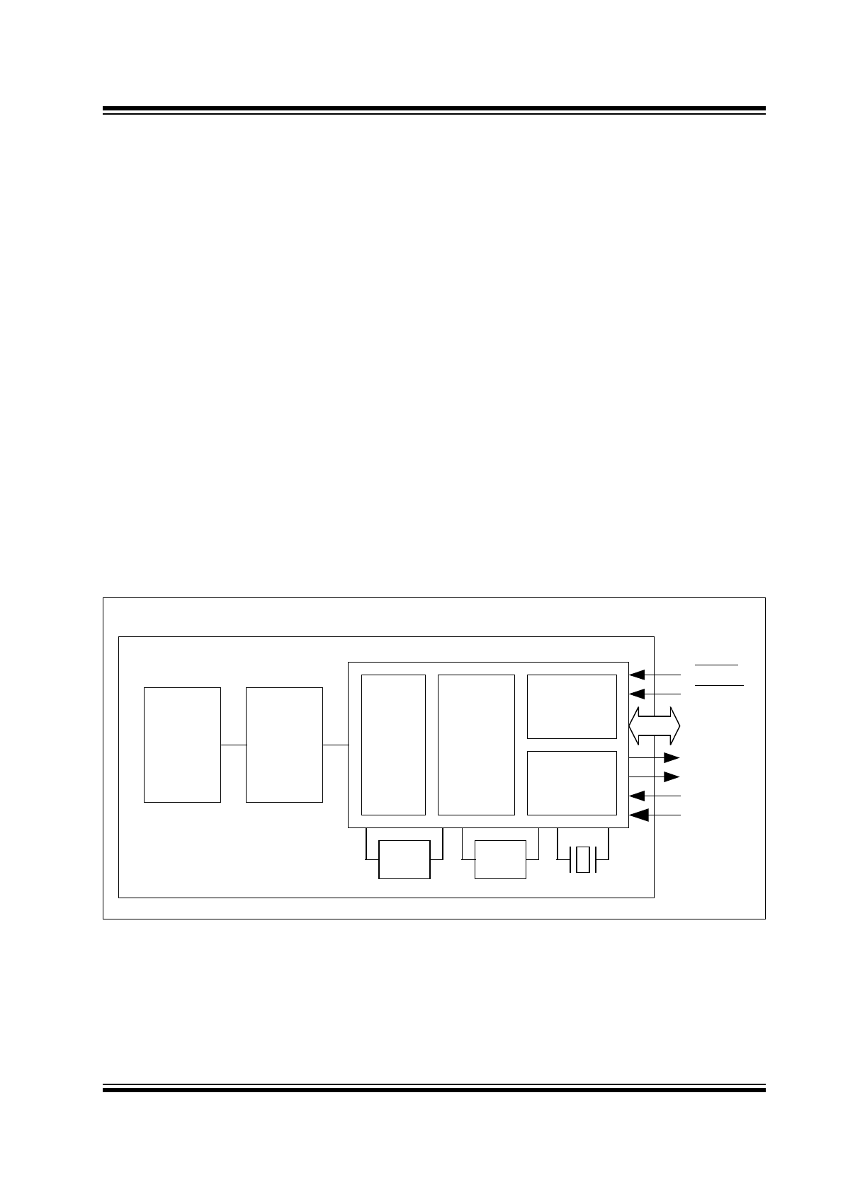
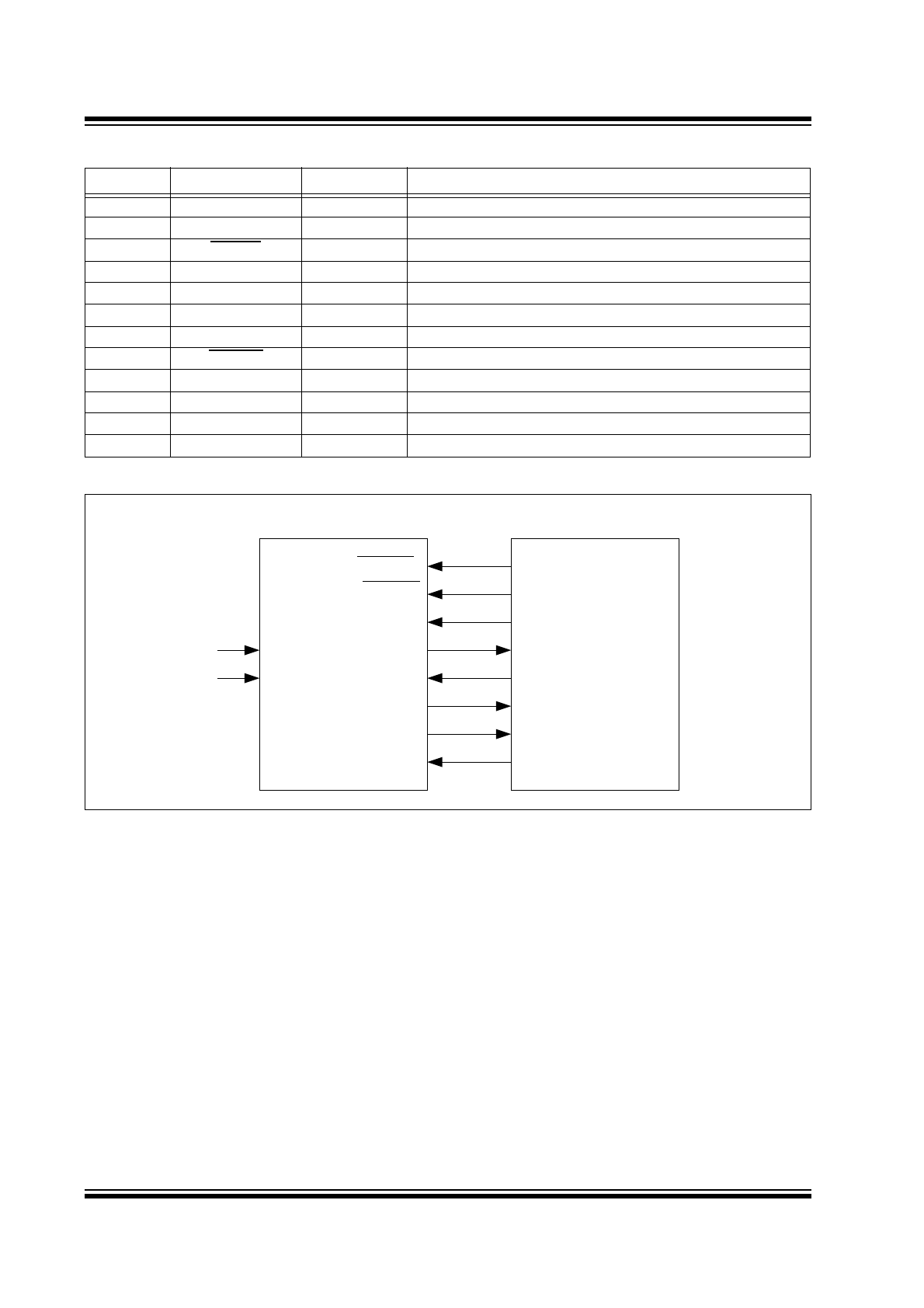
Interface description
The simplified block diagram of the MRF89XAM9A
module is shown in
Figure 1-1
. The module is based on
the Microchip Technology MRF89XA Ultra Low-Power
Sub-GHz Transceiver Integrated Circuit (IC). The
module interfaces to many popular Microchip PIC
®
microcontrollers through a 3-wire serial SPI interface,
two chip selects (configuration and data), two interrupts
Interrupt Request 0 (IRQ0) and Interrupt Request 1
(IRQ1), Reset, power and ground as shown in
Figure 1-2
.
Table 1-1
provides the pin descriptions.
Data communication and module configuration are
documented in the “MRF89XA Ultra Low-Power,
Integrated Sub-GHz Transceiver
” (DS70622) Data
Sheet. For more information on specific serial interface
protocol and general register definitions, refer to the
“MRF89XA Data Sheet” and see
Section 1.3,
Operation
for specific register settings unique to the
MRF89XAM9A module operation to maintain
regulatory compliance.
FIGURE 1-1:
MRF89XAM9A BLOCK DIAGRAM
MRF89XA
Control
Interface
Power
Management
Baseband
RF
MRF89XAM9A Module
SPI
Digital I/O
IRQ0
Power
12.8 MHz Crystal
Matching
Circuitry
and
SAW Filter
PCB
Antenna
Loop
Filter
VCO
Tank
IRQ1
CSDATA
CSCON
RESET
MRF89XAM9A
DS75017B-page 4
Preliminary
2011-2012 Microchip Technology Inc.
TABLE 1-1:
PIN DESCRIPTION
FIGURE 1-2:
MICROCONTROLLER TO MRF89XAM9A INTERFACE
Pin
Symbol
Type
Description
1
GND
Power
Ground
2
RESET
DI
Reset Pin. For more information, refer to
Section 1.3.1, Reset
3
CSCON
DI
Serial Interface Configure Chip Select
4
IRQ0
DO
Interrupt Request Output
5
SDI
DI
Serial Interface Data Input
6
SCK
DI
Serial Interface Clock
7
SDO
DO
Serial Interface Data Output
8
CSDATA
DI
Serial Interface Data Chip Select
9
IRQ1
DO
Interrupt Request Output
10
Vin
Power
Power Supply
11
GND
Power
Ground
12
GND
Power
Ground
PIC
®
Microcontroller
I/O
I/O
SDO
SDI
SCK
INTx
INTx
I/O
MRF89XAM9A
CSCON
CSDATA
SDI
SDO
SCK
IRQ0
IRQ1
RESET
V
IN
GND
2011-2012 Microchip Technology Inc.
Preliminary
DS75017B-page 5
MRF89XAM9A
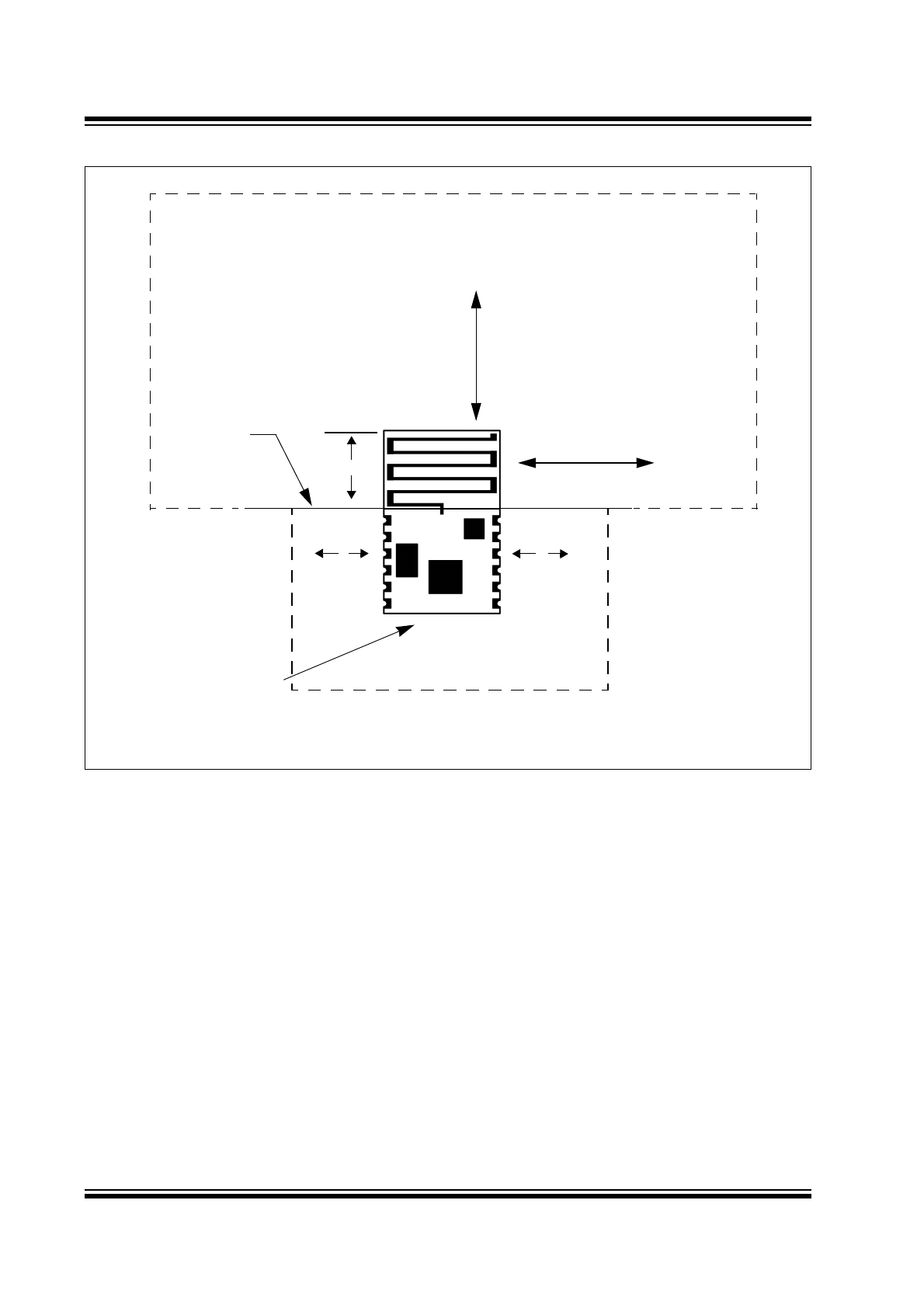
1.2
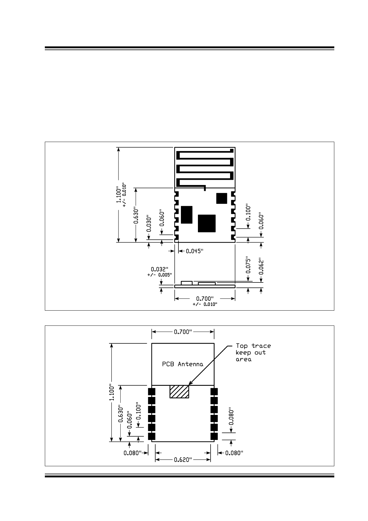
Mounting Details
The MRF89XAM9A is a surface mountable module.
The dimensions of the module are shown in
Figure 1-
3
. The module PCB is 0.032" thick with castellated
mounting holes on the edge.
Figure 1-4
is the
recommended host PCB footprint for the
MRF89XAM9A.
The MRF89XAM9A has an integrated PCB antenna.
For the best performance, follow the mounting details
shown in
Figure 1-5
. It is recommended that the
module be mounted on the edge of the host PCB and
an area around the antenna, approximately 3.4"
(8.6 cm), be kept clear of metal objects for best
performance. A host PCB ground plane around the
MRF89XAM9A acts as a counterpoise to the PCB
antenna. It is recommended to extend the ground plane
at least 0.4" (1 cm) around the module.
FIGURE 1-3:
MODULE DETAILS
FIGURE 1-4:
RECOMMENDED PCB FOOTPRINT
MRF89XAM9A
DS75017B-page 6
Preliminary
2011-2012 Microchip Technology Inc.
FIGURE 1-5:
MOUNTING DETAILS
3.4”
3.4”
0.4”
0.4”
Edge of PCB
0.470”
Keep area around the antenna,
approximately 3.4” (6.8 cm), be
kept clear of metallic objects for
best performance.
Host PCB top copper ground plane
(antenna counterpoise): Extend the
host PCB top copper ground plane
under and to the left and right side
of the module at least 0.4 inches
(1 cm) for best antenna
performance.

2011-2012 Microchip Technology Inc.
Preliminary
DS75017B-page 7
MRF89XAM9A
1.3
Operation
The MRF89XAM9A module is based on the
Microchip’s MRF89XA Ultra Low-Power, Integrated
ISM Band Sub-GHz Transceiver IC. Data
communication and module configuration are
documented in the “MRF89XA Ultra Low-Power,
Integrated ISM Band Sub-GHz Transceiver Data
Sheet
” (DS70622).
The following section emphasizes operational settings
that are unique to the MRF89XAM9A module design
that must be followed for the operation.
1.3.1
RESET
Pin 2 of the module, Reset, allows an external reset of
the MRF89XA IC. Reset is connected to the TEST8 pin
of the MRF89XA IC. During normal operations of the
MRF89XAM9A, the Reset pin should be held in a high
impedance state. For more information on assertion of
the RESET pin, refer to “Section 3.1.2 Manual Reset”
in the “MRF89XA Data Sheet” (DS70622).
1.3.2
CRYSTAL FREQUENCY
When calculating frequency deviation, bit rate, receiver
bandwidth, and PLL R, P and S values, use crystal
frequency f
xtal
= 12.8 MHz.
1.3.3
CLOCK OUTPUT (CLKOUT)
The CLKOUT pin 19 of the MRF89XA IC is not used on
the module. Ensure that the CLKOUT signal is disabled
to minimize current consumption.
1.3.4
FREQUENCY BAND SELECT
The Frequency Band Select bits (FBS<1:0>) in the
GCONREG<4:3> should be set for target channel
range 902–915 MHz FBS<1:0> = ‘00’ or 915–928 MHz
FBS<1:0> = ‘01’.
1.3.5
VCO TANK TRIM VALUE
The VCO Trim bits (VCOT<1:0>) in the
GCONREG<2:1> should be set for VCOT<1:0> = ‘01’
for the inductor values of the module.
1.3.6
BIT RATE
The maximum bit rate value will be limited to 28 kbps
for OOK modulation due to the crystal frequency of
12.8 MHz.

MRF89XAM9A
DS75017B-page 8
Preliminary
2011-2012 Microchip Technology Inc.
NOTES:
2011-2012 Microchip Technology Inc.
Preliminary
DS75017B-page 9
MRF89XAM9A
2.0
CIRCUIT DESCRIPTION
The MRF89XAM9A module interfaces to Microchip’s
PIC16, PIC18, PIC24, PIC32 and dsPIC33
microcontrollers with a minimum of external
components through digital only connections. An
example application schematic is shown in
Figure 2-1
.
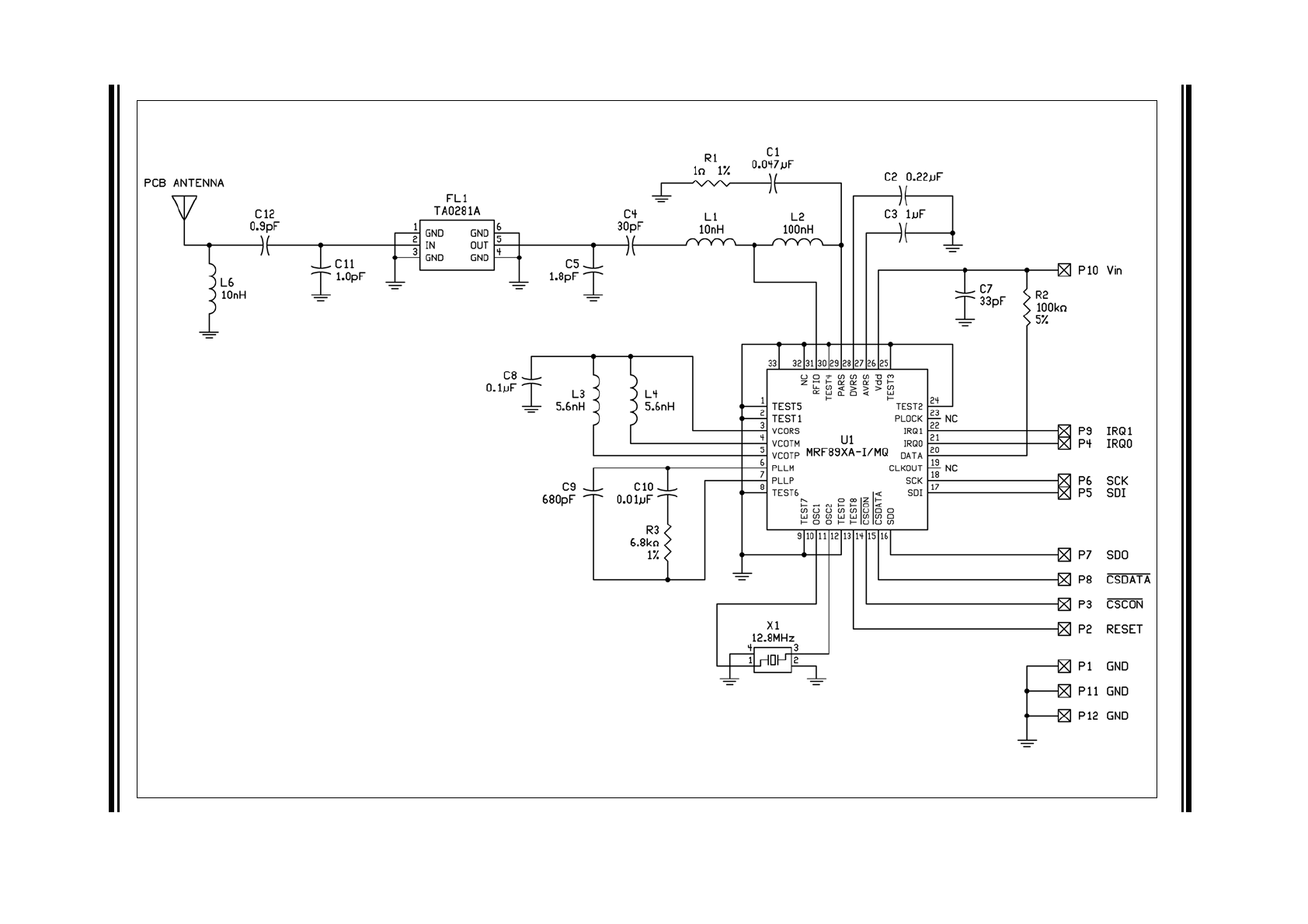
2.1
Module Schematic
The MRF89XAM9A module is based on the
Microchip’s MRF89XA Ultra Low-Power, Integrated
ISM Band Sub-GHz Transceiver IC. The serial I/O
(CSCON, CSDATA, SCK, SDO and SDI), Reset, IRQ0
and IRQ1 pins are routed out and available on the
module pins as shown in
Figure 2-2
. Crystal X1 is a
12.8 MHz crystal with a frequency tolerance of
±10 ppm at 25°C. The RFIO output is matched to the
SAW filter FL1 and further matched to the PCB trace
antenna.
Figure 2-2
illustrates the MRF89XAM9A schematics.
Table 2-1
details the Bill of Materials (BOM).
FIGURE 2-1:
MRF89XAM9A APPLICATION SCHEMATIC
Note 1
+ C2
1 0 μF
C1
0.1 μF
To Host
Microcontroller
To Host
Microcontroller
U1
MRF89XAM9A-I/RM
+ 3.3V
GND
RESET
CSCON
IRQ0
SDI
SCK
GND
GND
V
IN
IRQ1
CSDATA
SDO
1
2
3
4
5
6
12
11
10
9
8
7
Note:
For battery powered applications, place a 10 μF capacitor in parallel with the 0.1 μF bypass
capacitor to provide a low impedance during startup sequences.
MRF89XAM9A
DS75017B-
page 10
Prelimina
ry
2011-
2012 Microchip T
echnolo
gy Inc.
FIGURE 2-2:
MRF89XAM9A SCHEMATIC
Note:
Designators not used: C6, L5