

© 2010 Microchip Technology Inc.
Preliminary
DS70651A
MRF89XAM8A
Data Sheet
868 MHz Ultra-Low Power
Sub-GHz Transceiver Module
DS70651A-page ii
Preliminary
© 2010 Microchip Technology Inc.
Information contained in this publication regarding device
applications and the like is provided only for your convenience
and may be superseded by updates. It is your responsibility to
ensure that your application meets with your specifications.
MICROCHIP MAKES NO REPRESENTATIONS OR
WARRANTIES OF ANY KIND WHETHER EXPRESS OR
IMPLIED, WRITTEN OR ORAL, STATUTORY OR
OTHERWISE, RELATED TO THE INFORMATION,
INCLUDING BUT NOT LIMITED TO ITS CONDITION,
QUALITY, PERFORMANCE, MERCHANTABILITY OR
FITNESS FOR PURPOSE. Microchip disclaims all liability
arising from this information and its use. Use of Microchip
devices in life support and/or safety applications is entirely at
the buyer’s risk, and the buyer agrees to defend, indemnify and
hold harmless Microchip from any and all damages, claims,
suits, or expenses resulting from such use. No licenses are
conveyed, implicitly or otherwise, under any Microchip
intellectual property rights.
Trademarks
The Microchip name and logo, the Microchip logo, dsPIC,
K
EE
L
OQ
, K
EE
L
OQ
logo, MPLAB, PIC, PICmicro, PICSTART,
PIC
32
logo, rfPIC and UNI/O are registered trademarks of
Microchip Technology Incorporated in the U.S.A. and other
countries.
FilterLab, Hampshire, HI-TECH C, Linear Active Thermistor,
MXDEV, MXLAB, SEEVAL and The Embedded Control
Solutions Company are registered trademarks of Microchip
Technology Incorporated in the U.S.A.
Analog-for-the-Digital Age, Application Maestro, CodeGuard,
dsPICDEM, dsPICDEM.net, dsPICworks, dsSPEAK, ECAN,
ECONOMONITOR, FanSense, HI-TIDE, In-Circuit Serial
Programming, ICSP, Mindi, MiWi, MPASM, MPLAB Certified
logo, MPLIB, MPLINK, mTouch, Octopus, Omniscient Code
Generation, PICC, PICC-18, PICDEM, PICDEM.net, PICkit,
PICtail, REAL ICE, rfLAB, Select Mode, Total Endurance,
TSHARC, UniWinDriver, WiperLock and ZENA are
trademarks of Microchip Technology Incorporated in the
U.S.A. and other countries.
SQTP is a service mark of Microchip Technology Incorporated
in the U.S.A.
All other trademarks mentioned herein are property of their
respective companies.
© 2010, Microchip Technology Incorporated, Printed in the
U.S.A., All Rights Reserved.
Printed on recycled paper.
ISBN: 978-1-60932-637-1
Note the following details of the code protection feature on Microchip devices:
•
Microchip products meet the specification contained in their particular Microchip Data Sheet.
•
Microchip believes that its family of products is one of the most secure families of its kind on the market today, when used in the
intended manner and under normal conditions.
•
There are dishonest and possibly illegal methods used to breach the code protection feature. All of these methods, to our
knowledge, require using the Microchip products in a manner outside the operating specifications contained in Microchip’s Data
Sheets. Most likely, the person doing so is engaged in theft of intellectual property.
•
Microchip is willing to work with the customer who is concerned about the integrity of their code.
•
Neither Microchip nor any other semiconductor manufacturer can guarantee the security of their code. Code protection does not
mean that we are guaranteeing the product as “unbreakable.”
Code protection is constantly evolving. We at Microchip are committed to continuously improving the code protection features of our
products. Attempts to break Microchip’s code protection feature may be a violation of the Digital Millennium Copyright Act. If such acts
allow unauthorized access to your software or other copyrighted work, you may have a right to sue for relief under that Act.
Microchip received ISO/TS-16949:2002 certification for its worldwide
headquarters, design and wafer fabrication facilities in Chandler and
Tempe, Arizona; Gresham, Oregon and design centers in California
and India. The Company’s quality system processes and procedures
are for its PIC
®
MCUs and dsPIC
®
DSCs, K
EE
L
OQ
®
code hopping
devices, Serial EEPROMs, microperipherals, nonvolatile memory and
analog products. In addition, Microchip’s quality system for the design
and manufacture of development systems is ISO 9001:2000 certified.
© 2010 Microchip Technology Inc.
Preliminary
DS70651A-page 1
MRF89XAM8A
Features
• Module designed from the MRF89XA integrated
ultra low-power, sub-GHz transceiver IC.
• Supports proprietary sub-GHz wireless protocols
• Simple, SPI Interface with Interrupts
• Small size: 0.7" x 1.1" (17.8 mm x 27.9 mm),
surface mountable
• Integrated crystal, internal voltage regulator,
matching circuitry and Printed Circuit Board
(PCB) antenna
• Easy integration into final product: minimize prod-
uct development, quicker time to market
• Compatible with Microchip’s Microcontroller
families (PIC16, PIC18, PIC24, dsPIC33 and
PIC32)
• Conforms to the following ETSI standards:
- EN 300 220-2 V2.3.1 (2001–02)
- EN 301 489-3 V1.4.1 (2002–08)
Operational
• Operating voltage: 2.1–3.6V (3.3V typical)
• Temperature range: -40°C to +85°C Industrial
• Low-current consumption:
- Rx mode: 3 mA (typical)
- Tx mode: 25 mA at +10 dBm (typical)
- Sleep: 0.1 µA (typical)
RF/Analog Features
• 863–870 MHz operation
• Modulation: FSK and OOK
• Data rate (to conform to ETSI standards):
- FSK: 40 kbps
- OOK: 16 kbps
• Reception sensitivity
- FSK: -107 dBm (typical) at 25 kbps
- OOK: -113 dBm (typical) at 2 kbps
• +10 dBm typical output power with 21 dB Tx
power control range
Media Access Controller
(MAC)/Baseband Features
• Packet handling features with data whitening and
automatic CRC generation
• Incoming sync word (pattern) recognition
• Built-in bit synchronizer for incoming data, and clock
synchronization and recovery
• 64-byte transmit/receive FIFO with preload in stand-by
mode
• Supports Manchester encoding/decoding
techniques
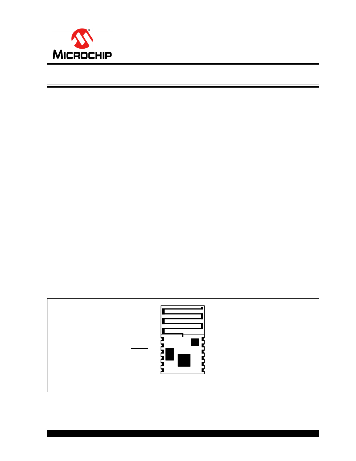
Pin diagram
2
3
4
5
6
1
7
V
IN
GND
8
9
10
RESET
CSCON
SDO
SDI
SCK
CSDATA
IRQ1
GND
IRQ0
12
11
GND
868 MHz Ultra-Low Power Sub-GHz Transceiver Module

MRF89XAM8A
DS70651A-page 2
Preliminary
© 2010 Microchip Technology Inc.
Table of Contents
.0
Device Overview .......................................................................................................................................................................... 3
2.0
Circuit Description ........................................................................................................................................................................ 9
3.0
Regulatory Approval................................................................................................................................................................... 19
4.0
Electrical Characteristics ............................................................................................................................................................ 21
Appendix A: Revision History............................................................................................................................................................... 27
The Microchip Web Site ....................................................................................................................................................................... 29
Customer Change Notification Service ................................................................................................................................................ 29
Customer Support ................................................................................................................................................................................ 29
Reader Response ................................................................................................................................................................................ 30
Product Identification System............................................................................................................................................................... 31
TO OUR VALUED CUSTOMERS
It is our intention to provide our valued customers with the best documentation possible to ensure successful use of your Microchip
products. To this end, we will continue to improve our publications to better suit your needs. Our publications will be refined and
enhanced as new volumes and updates are introduced.
If you have any questions or comments regarding this publication, please contact the Marketing Communications Department via
E-mail at docerrors@microchip.com or fax the Reader Response Form in the back of this data sheet to (480) 792-4150. We
welcome your feedback.
Most Current Data Sheet
To obtain the most up-to-date version of this data sheet, please register at our Worldwide Web site at:
http://www.microchip.com
You can determine the version of a data sheet by examining its literature number found on the bottom outside corner of any page.
The last character of the literature number is the version number, (e.g., DS30000A is version A of document DS30000).
Errata
An errata sheet, describing minor operational differences from the data sheet and recommended workarounds, may exist for current
devices. As device/documentation issues become known to us, we will publish an errata sheet. The errata will specify the revision
of silicon and revision of document to which it applies.
To determine if an errata sheet exists for a particular device, please check with one of the following:
• Microchip’s Worldwide Web site; http://www.microchip.com
• Your local Microchip sales office (see last page)
When contacting a sales office, please specify which device, revision of silicon and data sheet (include literature number) you are
using.
Customer Notification System
Register on our web site at www.microchip.com to receive the most current information on all of our products.
© 2010 Microchip Technology Inc.
Preliminary
DS70651A-page 3
MRF89XAM8A
1.0
DEVICE OVERVIEW
The MRF89XAM8A is an ultra-low power sub-GHz
surface mount transceiver module with integrated
crystal, internal voltage regulator, matching circuitry
and PCB antenna. The MRF89XAM8A module
operates in the European 863–870 MHz frequency
band and is ETSI compliant. The integrated module
design frees the integrator from the extensive RF and
antenna design, and regulatory compliance testing,
allowing quicker time to market.
The MRF89XAM8A module is compatible with
Microchip’s MiWi™ Development Environment
software stacks. The software stacks are available as a
free download, including source code, from the
Microchip’s web site
http://www.microchip.com/wireless
.
The MRF89XAM8A module has been tested and
conforms to EN 300 220-2 V2.3.1 (2001–02) and EN
301 489-3 V1.4.1 (2002–08) European Standards. The
module tests can be applied toward final product
certification and Declaration of Conformity (DoC). To
maintain conformance, refer to module settings in
Section 1.3, Operation
. Additional testing may be
required depending on the end application.
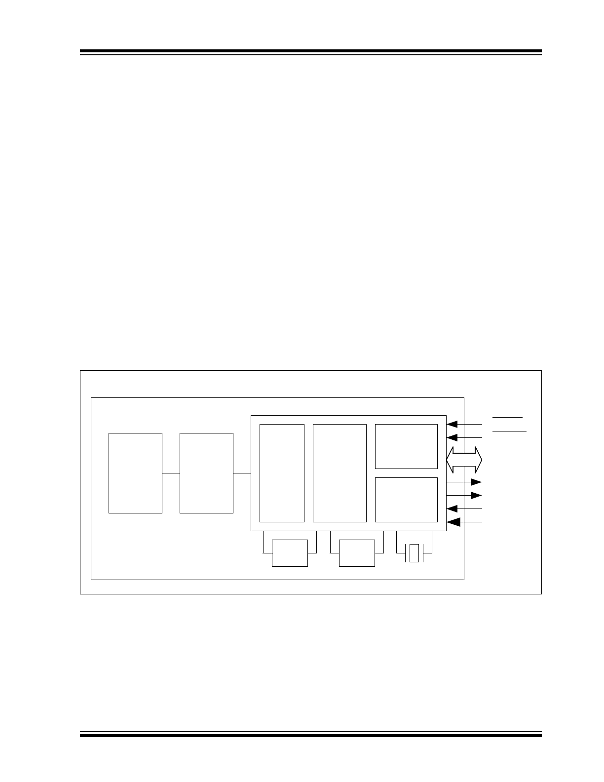
1.1
Interface description
The simplified block diagram of the MRF89XAM8A
module is illustrated in
Figure 1-1
. The module is based
on the Microchip Technology MRF89XA ultra-low
power sub-GHz transceiver Integrated Circuit (IC). The
module interfaces to many popular Microchip PIC
®
microcontrollers through a 3-wire serial SPI interface,
two chip selects (configuration and data), two interrupts
Interrupt Request 0 (IRQ0) and Interrupt Request 1
(IRQ1), Reset, power and ground as illustrated in
Figure 1-2
.
Table 1-1
provides the related pin
descriptions.
Serial communication and module configuration are
documented in the “MRF89XA Ultra-Low Power,
Integrated Sub-GHz Transceiver” (DS70622) Data
Sheet. Refer to the “MRF89XA Data Sheet” for specific
serial interface protocol and general register
definitions. Also, see
Section 1.3, Operation
for
specific register settings that are unique to the
MRF89XAM8A module operation to maintain
regulatory compliance.
FIGURE 1-1:
MRF89XAM8A BLOCK DIAGRAM
MRF89XA
Control
Interface
Power
Management
Baseband
RF
MRF89XAM8A Module
SPI
Digital I/O
IRQ0
Power
12.8 MHz Crystal
Matching
Circuitry
and
SAW Filter
PCB
Antenna
Loop
Filter
VCO
Tank
IRQ1
CSDATA
CSCON
RESET
MRF89XAM8A
DS70651A-page 4
Preliminary
© 2010 Microchip Technology Inc.
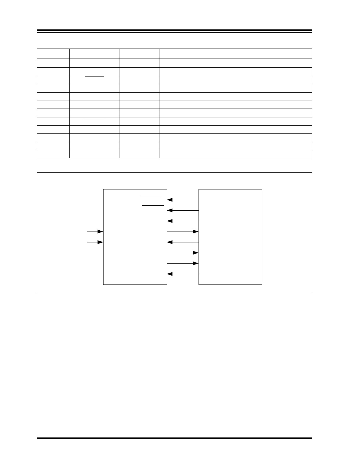
TABLE 1-1:
PIN DESCRIPTION
FIGURE 1-2:
MICROCONTROLLER TO MRF89XAM8A INTERFACE
Pin
Symbol
Type
Description
1
GND
Power
Ground
2
RESET
DI
Reset Pin
3
CSCON
DI
Serial Interface Configure Chip Select
4
IRQ0
DO
Interrupt Request Output
5
SDI
DI
Serial Interface Data Input
6
SCK
DI
Serial Interface Clock
7
SDO
DO
Serial Interface Data Output
8
CSDATA
DI
Serial Interface Data Chip Select
9
IRQ1
DO
Interrupt Request Output
10
Vin
Power
Power Supply
11
GND
Power
Ground
12
GND
Power
Ground
PIC
®
Microcontroller
I/O
I/O
SDO
SDI
SCK
INTx
INTx
I/O
MRF89XAM8A
CSCON
CSDATA
SDI
SDO
SCK
IRQ0
IRQ1
RESET
Vin
GND
© 2010 Microchip Technology Inc.
Preliminary
DS70651A-page 5
MRF89XAM8A
1.2
Mounting Details
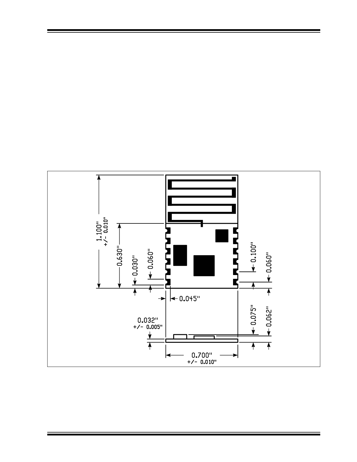
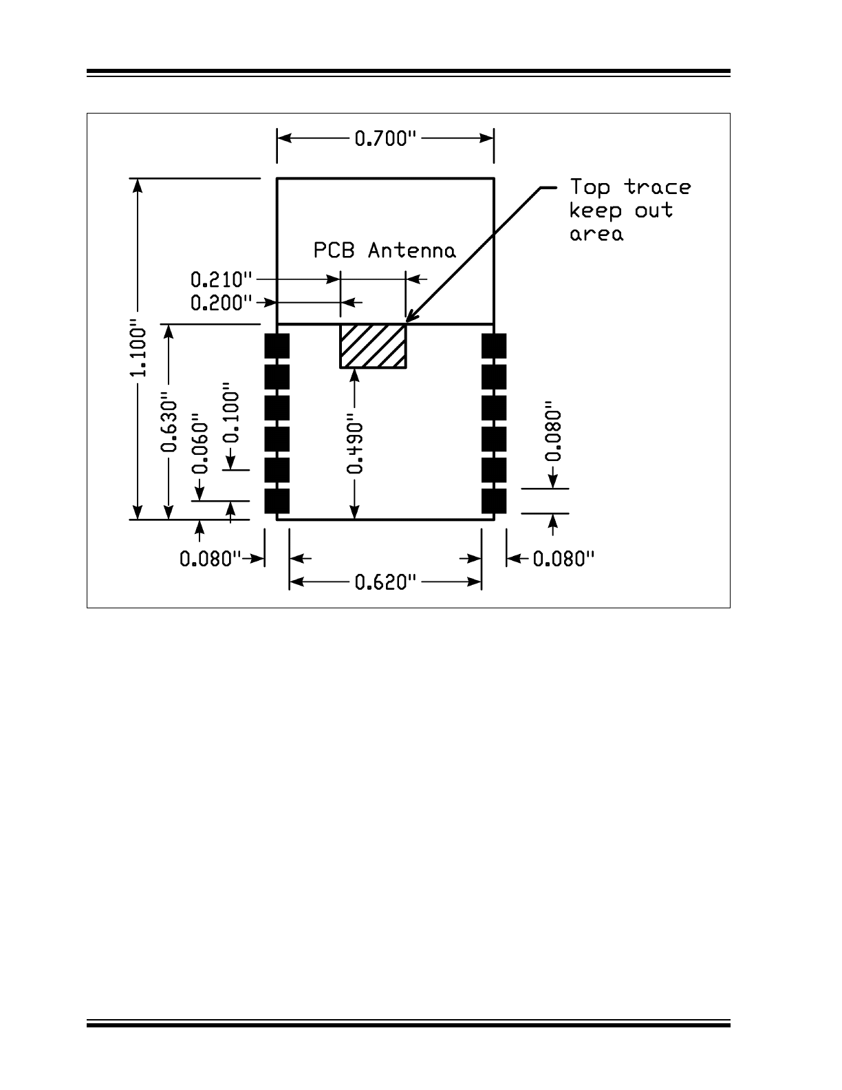
The MRF89XAM8A is a surface mountable module, the
module dimensions are illustrated in
Figure 1-3
. The
module PCB is 0.032" thick with castellated mounting
holes on the edge.
Figure 1-4
is the recommended host
PCB footprint for the MRF89XAM8A.
The MRF89XAM8A has an integrated PCB antenna.
For the best performance, follow the mounting details
as illustrated in
Figure 1-5
. It is recommended that the
module be mounted on the edge of the host PCB and
an area around the antenna, approximately 3.4" (8.6
cm), be kept clear of metal objects for best
performance. A host PCB ground plane around the
MRF89XAM8A acts as a counterpoise to the PCB
antenna. Extend the host PCB top copper ground plane
under and to the left and right side of the module at
least 0.4 inches (1 cm) for best antenna performance.
FIGURE 1-3:
MODULE DETAILS
MRF89XAM8A
DS70651A-page 6
Preliminary
© 2010 Microchip Technology Inc.
FIGURE 1-4:
RECOMMENDED PCB FOOTPRINT
© 2010 Microchip Technology Inc.
Preliminary
DS70651A-page 7
MRF89XAM8A
FIGURE 1-5:
MOUNTING DETAILS
3.4”
3.4”
0.4”
0.4”
Edge of PCB
0.470”
Keep area around antenna
(approximately 3.4 inches (8.6
cm)) clear of metallic structures
for best performance.
Host PCB Top Copper Ground
Plane (Antenna Counterpoise):
Extend the host PCB top copper
ground plane under and to the left
and right side of the module at
least 0.4 inches (1 cm) for best
antenna performance.

MRF89XAM8A
DS70651A-page 8
Preliminary
© 2010 Microchip Technology Inc.
1.3
Operation
The MRF89XAM8A module is based on the Microchip
Technology MRF89XA ultra-low power, integrated ISM
band sub-GHz transceiver IC. Serial communication
and module configuration are documented in the
“MRF89XA Ultra-Low Power, Integrated ISM Band
Sub-GHz Transceiver Data Sheet” (DS70622).
This section emphasizes operational settings that are
unique to the MRF89XAM8A module design that must
be followed in order for the module to conform to the
tested European standards summarized in
Section 3.0,
Regulatory Approval
.
1.3.1
RESET
Pin 2 of the module, RESET, enables an external reset
of the MRF89XA IC. RESET is connected to the TEST8
pin of the MRF89XA IC. During normal operations of
the MRF89XAM8A, the RESET pin should be held in a
high impedance state. For more information on
assertion of the RESET pin, refer to “Section 3.1.2
Manual Reset” of “MRF89XA Data Sheet” (DS70622).
1.3.2
CRYSTAL FREQUENCY
When calculating frequency deviation, bit rate, receiver
bandwidth, and PLL R, P and S values, use crystal
frequency f
xtal
= 12.8 MHz.
1.3.3
CLOCK OUTPUT (CLKOUT)
The CLKOUT pin 19 of the MRF89XA IC is not used on
the module. Ensure that the CLKOUT signal is disabled
to minimize current consumption.
1.3.4
FREQUENCY SHIFT KEYING
MODULATION (FSK)
The following settings must be followed for FSK
modulation mode to conform to the European
standards summarized in
Section 3.0, Regulatory
Approval
.
• Bit Rate Maximum Setting: 40 kbps
• Frequency Deviation Maximum Setting: 40 kHz
• Transmit Bandwidth Maximum Setting: 125 kHz
• Lower Frequency Setting: 863.5 MHz
• Upper Frequency Setting: 869.5 MHz
1.3.5
ON-OFF KEYING MODULATION
(OOK)
The following settings must be followed for OOK
modulation mode to conform to the European
standards summarized in
Section 3.0, Regulatory
Approval
.
• Bit Rate Maximum Setting: 16 kbps
• Frequency Deviation Maximum Setting: 80 kHz
• Transmit Bandwidth Maximum Setting: 125 kHz
• Lower Frequency Setting: 863.5 MHz
• Upper Frequency Setting: 869.5 MHz
Note:
To maintain conformance to tested ETSI
standards, the module shall not be
modified and settings in
Section 1.3,
Operation
must be observed.