
© 2009-2011 Microchip Technology Inc.
Preliminary
DS70590C
MRF49XA
Data Sheet
ISM Band Sub-GHz
RF Transceiver
DS70590C-page 2
Preliminary
© 2009-2011 Microchip Technology Inc.
Information contained in this publication regarding device
applications and the like is provided only for your convenience
and may be superseded by updates. It is your responsibility to
ensure that your application meets with your specifications.
MICROCHIP MAKES NO REPRESENTATIONS OR
WARRANTIES OF ANY KIND WHETHER EXPRESS OR
IMPLIED, WRITTEN OR ORAL, STATUTORY OR
OTHERWISE, RELATED TO THE INFORMATION,
INCLUDING BUT NOT LIMITED TO ITS CONDITION,
QUALITY, PERFORMANCE, MERCHANTABILITY OR
FITNESS FOR PURPOSE. Microchip disclaims all liability
arising from this information and its use. Use of Microchip
devices in life support and/or safety applications is entirely at
the buyer’s risk, and the buyer agrees to defend, indemnify and
hold harmless Microchip from any and all damages, claims,
suits, or expenses resulting from such use. No licenses are
conveyed, implicitly or otherwise, under any Microchip
intellectual property rights.
Trademarks
The Microchip name and logo, the Microchip logo, dsPIC,
K
EE
L
OQ
, K
EE
L
OQ
logo, MPLAB, PIC, PICmicro, PICSTART,
PIC
32
logo, rfPIC and UNI/O are registered trademarks of
Microchip Technology Incorporated in the U.S.A. and other
countries.
FilterLab, Hampshire, HI-TECH C, Linear Active Thermistor,
MXDEV, MXLAB, SEEVAL and The Embedded Control
Solutions Company are registered trademarks of Microchip
Technology Incorporated in the U.S.A.
Analog-for-the-Digital Age, Application Maestro, chipKIT,
chipKIT logo, CodeGuard, dsPICDEM, dsPICDEM.net,
dsPICworks, dsSPEAK, ECAN, ECONOMONITOR,
FanSense, HI-TIDE, In-Circuit Serial Programming, ICSP,
Mindi, MiWi, MPASM, MPLAB Certified logo, MPLIB,
MPLINK, mTouch, Omniscient Code Generation, PICC,
PICC-18, PICDEM, PICDEM.net, PICkit, PICtail, REAL ICE,
rfLAB, Select Mode, Total Endurance, TSHARC,
UniWinDriver, WiperLock and ZENA are trademarks of
Microchip Technology Incorporated in the U.S.A. and other
countries.
SQTP is a service mark of Microchip Technology Incorporated
in the U.S.A.
All other trademarks mentioned herein are property of their
respective companies.
© 2009-2011, Microchip Technology Incorporated, Printed in
the U.S.A., All Rights Reserved.
Printed on recycled paper.
ISBN: 978-1-61341-846-8
Note the following details of the code protection feature on Microchip devices:
•
Microchip products meet the specification contained in their particular Microchip Data Sheet.
•
Microchip believes that its family of products is one of the most secure families of its kind on the market today, when used in the
intended manner and under normal conditions.
•
There are dishonest and possibly illegal methods used to breach the code protection feature. All of these methods, to our
knowledge, require using the Microchip products in a manner outside the operating specifications contained in Microchip’s Data
Sheets. Most likely, the person doing so is engaged in theft of intellectual property.
•
Microchip is willing to work with the customer who is concerned about the integrity of their code.
•
Neither Microchip nor any other semiconductor manufacturer can guarantee the security of their code. Code protection does not
mean that we are guaranteeing the product as “unbreakable.”
Code protection is constantly evolving. We at Microchip are committed to continuously improving the code protection features of our
products. Attempts to break Microchip’s code protection feature may be a violation of the Digital Millennium Copyright Act. If such acts
allow unauthorized access to your software or other copyrighted work, you may have a right to sue for relief under that Act.
Microchip received ISO/TS-16949:2009 certification for its worldwide
headquarters, design and wafer fabrication facilities in Chandler and
Tempe, Arizona; Gresham, Oregon and design centers in California
and India. The Company’s quality system processes and procedures
are for its PIC
®
MCUs and dsPIC
®
DSCs, K
EE
L
OQ
®
code hopping
devices, Serial EEPROMs, microperipherals, nonvolatile memory and
analog products. In addition, Microchip’s quality system for the design
and manufacture of development systems is ISO 9001:2000 certified.

© 2009-2011 Microchip Technology Inc.
Preliminary
DS70590C-page 3
MRF49XA
Features
• Fully Integrated Sub-GHz Transceiver
• Supports Proprietary Sub-GHz Wireless Protocols
• 4-Wire Serial Peripheral Interface (SPI)
Compatible Interface
• CMOS/TTL Compatible I/Os
• Clock and Reset Signals for Microcontroller
• Integrated 10 MHz Oscillator Circuitry
• Integrated Low Battery Voltage Detector
• Supports Power-Saving modes
• Operating Voltage: 2.2V–3.8V
• Low-Current Consumption, Typically:
- 11 mA in RX mode
- 15 mA in TX mode
- 0.3
μA in Sleep mode
• Industrial Temperature Range
• 16-Pin TSSOP Package
RF/Analog Features
• Supports ISM Band Sub-GHz Frequency Ranges
(433 MHz, 868 MHz and 915 MHz)
• Modulation Technique: FSK with Frequency
Hopping Spread Spectrum (FHSS) Capability
• Supports High Data Rates:
- Digital mode 115.2 kbps, max.
- Analog mode 256 kbps, max.
• Differential RF Input/Output:
- -110 dBm Typical Sensitivity with 0 dBm
Maximum Input Level
- +7 dBm Typical Transmit Output Power
• High-Resolution Programmable Phase-Locked
Loop (PLL) Synthesizer
• Integrated Power Amplifier
• Integrated Low Phase Noise Voltage Controlled
Oscillator (VCO) Frequency
• Synthesizer and PLL Loop Filter
• Automatic Frequency Control (AFC)
Baseband Features
• Supports Programmable TX Frequency Deviation
and RX Baseband Bandwidth (BBBW)
• Analog and Digital RSSI Outputs with Dynamic
Range
• RX Synchronous Pattern Recognition
• 16-Bit RX Data FIFO
• Two 8-Bit TX Data Registers
• Low-Power Duty Cycle mode
• Advanced Adjacent Channel Rejection/Blocking
Capability
• Internal Data and Clock Recovery
• Supports Data Filtering
• Data Quality Indicator (DQI)
Typical Applications
• Home/Industrial Automation
• Remote Control
• Wireless PC Peripherals
• Remote Keyless Entry
• Vehicle Sensor Monitoring
• Telemetry
• Data Logging Systems
• Remote Automatic Meter Reading
• Security Systems for Home/Industrial
Environment
• Automobile Immobilizers
• Sports and Performance Monitoring
• Wireless Toy Controls
• Medical Applications
ISM Band Sub-GHz RF Transceiver
MRF49XA
DS70590C-page 4
Preliminary
© 2009-2011 Microchip Technology Inc.
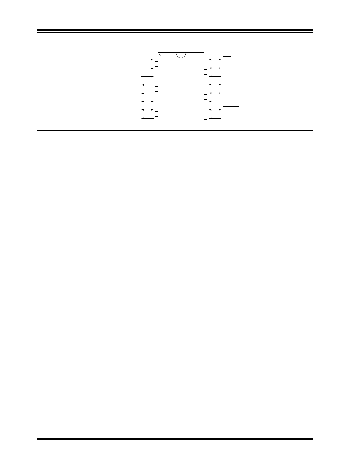
Pin Diagram: 16-Pin TSSOP
INT/DIO
RSSIO
V
DD
RFN
RFP
V
SS
RESET
RFXTL/EXTREF
SDI
SCK
CS
SDO
IRQ
FSK/DATA/FSEL
RCLKOUT/FCAP/FINT
CLKOUT
1
2
3
4
5
6
7
8
16
15
14
13
12
11
10
9
MRF49XA

© 2009-2011 Microchip Technology Inc.
Preliminary
DS70590C-page 5
MRF49XA
Table of Contents
1.0
Introduction................................................................................................................................................................................... 7
2.0
Hardware Description................................................................................................................................................................... 9
3.0
Functional Description................................................................................................................................................................ 43
4.0
Application Details...................................................................................................................................................................... 73
5.0
Electrical Characteristics ............................................................................................................................................................ 79
6.0
Packaging Information................................................................................................................................................................ 89
Appendix A: Read Sequence and Packet Structures .......................................................................................................................... 93
Appendix B: Revision History............................................................................................................................................................... 95
The Microchip Web Site....................................................................................................................................................................... 99
Customer Change Notification Service ................................................................................................................................................ 99
Customer Support................................................................................................................................................................................ 99
Reader Response .............................................................................................................................................................................. 100
Product Identification System ............................................................................................................................................................ 101
TO OUR VALUED CUSTOMERS
It is our intention to provide our valued customers with the best documentation possible to ensure successful use of your Microchip
products. To this end, we will continue to improve our publications to better suit your needs. Our publications will be refined and
enhanced as new volumes and updates are introduced.
If you have any questions or comments regarding this publication, please contact the Marketing Communications Department via
E-mail at
docerrors@microchip.com
or fax the Reader Response Form in the back of this data sheet to (480) 792-4150. We
welcome your feedback.
Most Current Data Sheet
To obtain the most up-to-date version of this data sheet, please register at our Worldwide Web site at:
http://www.microchip.com
You can determine the version of a data sheet by examining its literature number found on the bottom outside corner of any page.
The last character of the literature number is the version number, (e.g., DS30000A is version A of document DS30000).
Errata
An errata sheet, describing minor operational differences from the data sheet and recommended workarounds, may exist for current
devices. As device/documentation issues become known to us, we will publish an errata sheet. The errata will specify the revision
of silicon and revision of document to which it applies.
To determine if an errata sheet exists for a particular device, please check with one of the following:
• Microchip’s Worldwide Web site;
http://www.microchip.com
• Your local Microchip sales office (see last page)
When contacting a sales office, please specify which device, revision of silicon and data sheet (include literature number) you are
using.
Customer Notification System
Register on our web site at
www.microchip.com
to receive the most current information on all of our products.

MRF49XA
DS70590C-page 6
Preliminary
© 2009-2011 Microchip Technology Inc.
NOTES:

© 2009-2011 Microchip Technology Inc.
Preliminary
DS70590C-page 7
MRF49XA
1.0
INTRODUCTION
Microchip’s MRF49XA is a fully integrated Sub-GHz
RF transceiver. This low-power single chip Frequency
Shift Keying (FSK) baseband transceiver supports:
• Zero-IF architecture
• Multi-channel and multi-band
• Synthesizer with PLL
• Power Amplifier (PA)
• Low Noise Amplifier (LNA)
• I/Q down converter mixers
• I/Q demodulator
• Baseband filters (BBFs) and amplifiers
The simplified functional block diagram of MRF49XA is
shown in
Figure 1-1
. The MRF49XA is an ideal choice
for low-cost, high-volume, low data rate (<256 kbps),
two-way and short range wireless applications. This
transceiver can be used in the unlicensed 433 MHz,
868 MHz and 915 MHz frequency bands, and for
applications looking for FCC, IC or ETSI certification in
the ISM band.
The MRF49XA has a low phase noise and provides an
excellent adjacent channel interference, Bit Error Rate
(BER) and larger communication coverage along with
higher output power. The MRF49XA device’s AFC
feature allows for the use of a low-accuracy, low-cost
crystal. In order to minimize the total system cost, a
communication link in most of the applications can be
created using a low-cost, generic 10 MHz crystal, a
bypass filter and an affordable microcontroller. The
MRF49XA provides a clock signal for the
microcontroller and avoids the need for a second
crystal on the circuit board. The transceiver can be
interfaced with many popular Microchip PIC
®
microcontrollers through a 4-wire SPI, interrupt (IRO)
and Reset. The interface between the microcontroller
and MRF49XA is shown in
Figure 1-2
.
The MRF49XA supports the following digital data
processing features:
• PLL and I/Q VCO with Calibration
• Receiver Signal Strength Indicator
• Data Quality Indicator
• AFC
• Baseband Power Amplifier
• TX and RX Buffers
The receiver’s Baseband Bandwidth (BBBW) can be
programmed to accommodate various deviations, data
rates and crystal tolerance requirements.
The high-resolution PLL allows:
• The usage of multiple channels in any of the
bands
• The rapid settling time allows for faster frequency
hopping, bypassing multipath fading and
interference to achieve robust wireless links
The transceiver is integrated with different Sleep modes
and an internal wake-up timer to reduce the overall
current consumption, and to extend the battery life. The
device’s small size with low-power consumption makes
it ideal for various short range radio applications.
MRF49XA
DS70590C-page 8
Preliminary
© 2009-2011 Microchip Technology Inc.
FIGURE 1-1:
FUNCTIONAL NODE BLOCK DIAGRAM
FIGURE 1-2:
MICROCONTROLLER TO MRF49XA INTERFACE
Matching
Circuitry
Antenna
10 MHz
MCU
Interface
RFP
RFN
MRF49XA
Power
Management
Memory
PA/LNA
and
PLL/CLK
Block
RF Block
Baseband
Amplifier/
Filter/
Limiter
Data
Processing
Unit
SPI
Signals
Other
Handshaking
Signals
SDO
SDI
SCK
I/O
I/O
PIC® MCU
SDI
SDO
SCK
I/O
CLKOUT*
OSC1
IRO
RCLKOUT/FCAP/FINT*
I/O
MRF49XA
* Implies optional signals.
CS
__
INT
I/O/SS
RESET*
INT/DIO*
FSK/DATA/FSEL*

© 2009-2011 Microchip Technology Inc.
Preliminary
DS70590C-page 9
MRF49XA
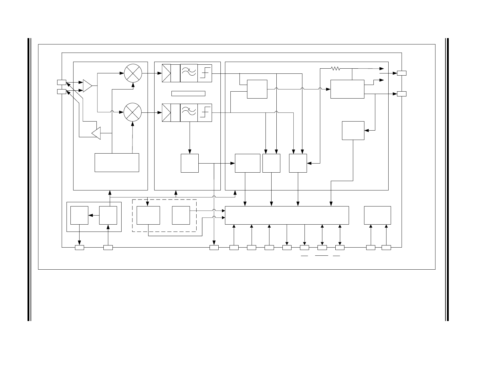
2.0
HARDWARE DESCRIPTION
The MRF49XA is an integrated, single chip ISM Band
Sub-GHz Transceiver. A simplified architectural block
diagram of the MRF49XA is shown in
Figure 2-1
.
The frequency synthesizer is clocked by an external
10 MHz crystal and generates the 433, 868 and 915
MHz radio frequency. The receiver with a Zero-IF
architecture consists of the following components:
• LNA
• Down Conversion Mixers
• Channel Filters
• Baseband Limiting Amplifiers
• Receiver Signal Strength Indicator
The transmitter with a direct conversion architecture
has a typical output power of +7 dBm. An internal
transmit/receive switch combines the transmitter and
receiver circuits into differential RFP and RFN pins.
These pins are connected to the impedance matching
circuitry (Balun) and to the external antenna connected
to the device.
The device operates in the low-voltage range of 2.2V–
3.8V, and in Sleep mode, it operates at a very low-current
state, typically 0.3 μA.
The quality of the data is checked or validated using the
RSSI and DQI blocks built into the transceiver. Data is
buffered in transmitter registers and receiver FIFOs.
The AFC feature allows the use of a low-accuracy and
low-cost crystal. The CLKOUT is used to clock the
external controller. The transceiver is controlled through
a 4-wire SPI, interrupt (INT/DIO and IRO),
FSK/DATA/FSEL, RCLKOUT/FCAP/FINT and RESET
pins. See
Table 2-1
for pin details.
The MRF49XA supports the following feature blocks:
• Clock Generation
• Data Filtering and Amplification
• Data Pattern Recognition and Timing
• Data Processing and Storage
• Independent Transmit and Receiver FIFO Buffers
• Registers
These features reduce the processing load, and hence,
allows the use of low-cost 8-bit microcontrollers for data
processing.
MRF49XA
DS70590C
-page 10
Prelimina
ry
©
2009-
2011 Microchip T
echnolo
gy Inc.
FIGURE 2-1:
MRF49XA ARCHITECTURAL BLOCK DIAGRAM
8
PA/LNA and PLL/CLK
Block
Baseband Amplifier/Filter/Limiter
Block
Low-Power Block
Microcontroller Interface Block
Power
Supply Block
Data Processing Block
AFC
DQI
Comparator
FIFO
Data Filtering
and Clock
Recovery Unit
I/Q
DEMOD
LBDB
WUTM
with
calibration
OSC
CLK
RSSI
1
3
2
4
10
5
16
14
11
9
15
Self Calibration
PLL and I/Q VCO with
Calibration
MIX
MIX
12
13
6
7
CLK
DATA
SDI
SCK
SDO
FSK/DATA/
FSEL
RCLKOUT/
FCAP/FINT
CLKOUT
RSSIO
V
DD
V
SS
RFP
RFN
RFXTL/
EXTREF
I
Q
____
Clock Block
LNA
PA
AMP
Cal
Ckt
AMP
Cal
Ckt
IRO
CS
__
INT/DIO
RESET