

© 2011 Microchip Technology Inc.
Preliminary
DS75002A
MRF24J40MC
Data Sheet
2.4 GHz IEEE Std. 802.15.4™ RF
Transceiver Module with PA/LNA and
External Antenna Connector
DS75002A-page ii
Preliminary
© 2011 Microchip Technology Inc.
Information contained in this publication regarding device
applications and the like is provided only for your convenience
and may be superseded by updates. It is your responsibility to
ensure that your application meets with your specifications.
MICROCHIP MAKES NO REPRESENTATIONS OR
WARRANTIES OF ANY KIND WHETHER EXPRESS OR
IMPLIED, WRITTEN OR ORAL, STATUTORY OR
OTHERWISE, RELATED TO THE INFORMATION,
INCLUDING BUT NOT LIMITED TO ITS CONDITION,
QUALITY, PERFORMANCE, MERCHANTABILITY OR
FITNESS FOR PURPOSE. Microchip disclaims all liability
arising from this information and its use. Use of Microchip
devices in life support and/or safety applications is entirely at
the buyer’s risk, and the buyer agrees to defend, indemnify and
hold harmless Microchip from any and all damages, claims,
suits, or expenses resulting from such use. No licenses are
conveyed, implicitly or otherwise, under any Microchip
intellectual property rights.
Trademarks
The Microchip name and logo, the Microchip logo, dsPIC,
K
EE
L
OQ
, K
EE
L
OQ
logo, MPLAB, PIC, PICmicro, PICSTART,
PIC
32
logo, rfPIC and UNI/O are registered trademarks of
Microchip Technology Incorporated in the U.S.A. and other
countries.
FilterLab, Hampshire, HI-TECH C, Linear Active Thermistor,
MXDEV, MXLAB, SEEVAL and The Embedded Control
Solutions Company are registered trademarks of Microchip
Technology Incorporated in the U.S.A.
Analog-for-the-Digital Age, Application Maestro, CodeGuard,
dsPICDEM, dsPICDEM.net, dsPICworks, dsSPEAK, ECAN,
ECONOMONITOR, FanSense, HI-TIDE, In-Circuit Serial
Programming, ICSP, Mindi, MiWi, MPASM, MPLAB Certified
logo, MPLIB, MPLINK, mTouch, Octopus, Omniscient Code
Generation, PICC, PICC-18, PICDEM, PICDEM.net, PICkit,
PICtail, REAL ICE, rfLAB, Select Mode, Total Endurance,
TSHARC, UniWinDriver, WiperLock and ZENA are
trademarks of Microchip Technology Incorporated in the
U.S.A. and other countries.
SQTP is a service mark of Microchip Technology Incorporated
in the U.S.A.
All other trademarks mentioned herein are property of their
respective companies.
© 2011, Microchip Technology Incorporated, Printed in the
U.S.A., All Rights Reserved.
Printed on recycled paper.
ISBN: 978-1-61341-006-6
Note the following details of the code protection feature on Microchip devices:
•
Microchip products meet the specification contained in their particular Microchip Data Sheet.
•
Microchip believes that its family of products is one of the most secure families of its kind on the market today, when used in the
intended manner and under normal conditions.
•
There are dishonest and possibly illegal methods used to breach the code protection feature. All of these methods, to our
knowledge, require using the Microchip products in a manner outside the operating specifications contained in Microchip’s Data
Sheets. Most likely, the person doing so is engaged in theft of intellectual property.
•
Microchip is willing to work with the customer who is concerned about the integrity of their code.
•
Neither Microchip nor any other semiconductor manufacturer can guarantee the security of their code. Code protection does not
mean that we are guaranteeing the product as “unbreakable.”
Code protection is constantly evolving. We at Microchip are committed to continuously improving the code protection features of our
products. Attempts to break Microchip’s code protection feature may be a violation of the Digital Millennium Copyright Act. If such acts
allow unauthorized access to your software or other copyrighted work, you may have a right to sue for relief under that Act.
Microchip received ISO/TS-16949:2002 certification for its worldwide
headquarters, design and wafer fabrication facilities in Chandler and
Tempe, Arizona; Gresham, Oregon and design centers in California
and India. The Company’s quality system processes and procedures
are for its PIC
®
MCUs and dsPIC
®
DSCs, K
EE
L
OQ
®
code hopping
devices, Serial EEPROMs, microperipherals, nonvolatile memory and
analog products. In addition, Microchip’s quality system for the design
and manufacture of development systems is ISO 9001:2000 certified.
© 2011 Microchip Technology Inc.
Preliminary
DS75002A-page 3
MRF24J40MC
Features:
• IEEE Std. 802.15.4™ Compliant RF Transceiver
• Supports ZigBee
®
, MiWi™ Development
Environment Proprietary Wireless Networking
Protocols
• 4-Wire Serial Peripheral Interface (SPI) with
Interrupt
• Small size: 0.9" x 1.3" (22.9 mm x 33.0 mm),
Surface Mountable : Pin Compatible with
MRF24J40MB
• Integrated Crystal, Internal Voltage Regulator,
Matching Circuitry, Power Amplifier, Low Noise
Amplifier
• External Antenna Connector : Ultra Miniature
Coaxial (U.FL), 50Ω
• Easy Integration into Final Product : Minimize
Product Development, Quicker Time to Market
• Radio Regulation Certified for United States
(FCC), Canada (IC), Europe (ETSI) and
Australia/New Zealand (C-TICK)
• Compatible with Microchip microcontroller
families (PIC16, PIC18, PIC24, dsPIC33 and
PIC32)
• Range up to 4000 ft
Operational:
• Operating Voltage: 2.7V – 3.6V (3.3V typical)
• Temperature Range: -40°C to +85°C Industrial
• Low-Current Consumption:
- Rx Mode: 25 mA (typical)
- Tx Mode: 120 mA (typical)
- Sleep: 12
μA (typical)
RF/Analog Features:
• ISM Band 2.405 GHz – 2.475 GHz Operation
• Data Rate: 250 kbps
• -108 dBm Typical Sensitivity with -23 dBm
Maximum Input Level
• +19 dBm Typical Output Power with 45 dB Tx
Power Control Range
• Integrated Low Phase Noise VCO, Frequency
Synthesizer and PLL Loop Filter
• Digital VCO and Filter Calibration
• Integrated RSSI ADC and I/Q DACs
• Integrated LDO
• High Receiver RSSI Dynamic Range
MAC/Baseband Features:
• Hardware CSMA-CA Mechanism, Automatic ACK
Response and FCS Check
• Independent Beacon, Transmit and GTS FIFO
• Supports all CCA modes and RSS/LQI
• Automatic Packet Retransmit Capable
• Hardware Security Engine (AES-128) with CTR,
CCM and CBC-MAC modes
• Supports Encryption and Decryption for MAC Sub
layer and Upper Layer
Pin Diagram:
2
3
4
5
6
1
7
V
IN
GND
8
9
10
RESET
WAKE
SDO
SDI
SCK
CS
NC
GND
INT
12
11
GND
2.4 GHz IEEE Std. 802.15.4™ RF Transceiver Module with
PA/LNA and External Antenna Connector

MRF24J40MC
DS75002A-page 4
Preliminary
© 2011 Microchip Technology Inc.
Table of Contents
1.0
Device Overview .......................................................................................................................................................................... 5
2.0
Circuit Description ...................................................................................................................................................................... 11
3.0
Regulatory Approval................................................................................................................................................................... 17
4.0
Electrical Characteristics ........................................................................................................................................................... 23
Appendix A: Revision History............................................................................................................................................................... 25
The Microchip Web Site ....................................................................................................................................................................... 27
Customer Change Notification Service ................................................................................................................................................ 27
Customer Support ................................................................................................................................................................................ 27
Reader Response ................................................................................................................................................................................ 28
Product Identification System............................................................................................................................................................... 29
TO OUR VALUED CUSTOMERS
It is our intention to provide our valued customers with the best documentation possible to ensure successful use of your Microchip
products. To this end, we will continue to improve our publications to better suit your needs. Our publications will be refined and
enhanced as new volumes and updates are introduced.
If you have any questions or comments regarding this publication, please contact the Marketing Communications Department via
E-mail at
docerrors@microchip.com
or fax the Reader Response Form in the back of this data sheet to (480) 792-4150. We
welcome your feedback.
Most Current Data Sheet
To obtain the most up-to-date version of this data sheet, please register at our Worldwide Web site at:
http://www.microchip.com
You can determine the version of a data sheet by examining its literature number found on the bottom outside corner of any page.
The last character of the literature number is the version number, (e.g., DS30000A is version A of document DS30000).
Errata
An errata sheet, describing minor operational differences from the data sheet and recommended workarounds, may exist for current
devices. As device/documentation issues become known to us, we will publish an errata sheet. The errata will specify the revision
of silicon and revision of document to which it applies.
To determine if an errata sheet exists for a particular device, please check with one of the following:
• Microchip’s Worldwide Web site;
http://www.microchip.com
• Your local Microchip sales office (see last page)
When contacting a sales office, please specify which device, revision of silicon and data sheet (include literature number) you are
using.
Customer Notification System
Register on our web site at
www.microchip.com
to receive the most current information on all of our products.
© 2011 Microchip Technology Inc.
Preliminary
DS75002A-page 5
MRF24J40MC
1.0
DEVICE OVERVIEW
The MRF24J40MC is a 2.4 GHz IEEE Std. 802.15.4™
compliant, surface mount module with integrated
crystal, internal voltage regulator, matching circuitry,
Power Amplifier (PA), Low Noise Amplifier (LNA) with
50Ω external antenna connector. The MRF24J40MC
module operates in the non-licensed 2.4 GHz
frequency band. The integrated module design frees
the integrator from extensive RF and antenna design,
and regulatory compliance testing allowing quicker
time to market.
The MRF24J40MC module is compatible with
Microchip’s ZigBee
®
, and MiWi™ Development
Environment software stacks. The MiWi Development
Environment software stack including the source code
is available as a free download, from the Microchip web
site:
http://www.microchip.com/wireless
.
The MRF24J40MC module has received regulatory
approvals for modular devices in the United States
(FCC) and Canada (IC). Modular approval removes the
need for expensive RF and antenna design, and allows
the end user to place the MRF24J40MC module inside
a finished product and does not require regulatory
testing for an intentional radiator (RF transmitter). To
maintain conformance, refer to module settings in
Section 3.1.1 “MRF24J40MC Settings”
for the
United States and
Section 3.2.1 “MRF24J40MC
Settings”
for Canada.
The MRF24J40MC module has been tested and
conforms to ETS EN 300 328 V1.7.1 (2006-10)
European Standards. The module tests can be applied
toward final product certification and Declaration of
Conformity (DoC). To maintain conformance for
Europe, refer to module settings in
Section 3.3.1
“MRF24J40MC Settings”
. Additional testing may be
required depending on the end application.
1.1
Interface Description
Figure 1-1
shows a simplified block diagram of the
MRF24J40MC module. The module is based on the
Microchip Technology MRF24J40 IEEE 802.15.4™
2.4 GHz RF Transceiver IC. The module interfaces to
many popular Microchip PIC
®
microcontrollers
through a 4-wire SPI interface, interrupt, wake, reset,
power and ground, as shown in
Figure 1-2
.
Table 1-1
provides the pin descriptions.
Serial communication and module configuration for the
MRF24J40MC module are documented in the
“MRF24J40 Data Sheet” (DS39776). Refer to the
datasheet for specific serial interface protocol and
register definitions.
Also, see
Section 1.3 “Operation”
for specific register
settings that are unique to the MRF24J40MC module.
FIGURE 1-1:
PIC18FXXXX BLOCK DIAGRAM
Antenna
U.FL
PA
Physical
MAC
Interface
Power
Management
SPI
20 MHz
Crystal
Digital
I/O
Power
PIC18FXXXX IEEE Std. 802.15.4™ Module
MRF24J40
LNA
Connector
MRF24J40MC
DS75002A-page 6
Preliminary
© 2011 Microchip Technology Inc.
FIGURE 1-2:
MICROCONTROLLER TO MRF24J40MC INTERFACE
TABLE 1-1:
PIN DESCRIPTION
Pin
Symbol
Type
Description
1
GND
Ground
Ground
2
RESET
DI
Global hardware Reset pin
3
WAKE
DI
External wake-up trigger
4
INT
DO
Interrupt pin to microcontroller
5
SDI
DI
Serial interface data input
6
SCK
DI
Serial interface clock
7
SDO
DO
Serial interface data output from MRF24J40
8
CS
DI
Serial interface enable
9
NC
—
No connection
10
V
IN
Power
Power supply
11
GND
Ground
Ground
12
GND
Ground
Ground
Legend: Pin type abbreviation: D = Digital, I = Input, O = Output
SDO
I/O
SDI
SCK
INTX
MRF24J40MC
CS
SDI
SDO
SCK
INT
I/O
WAKE
V
IN
GND
PIC
®
MCU
I/O
RESET
© 2011 Microchip Technology Inc.
Preliminary
DS75002A-page 7
MRF24J40MC
1.2
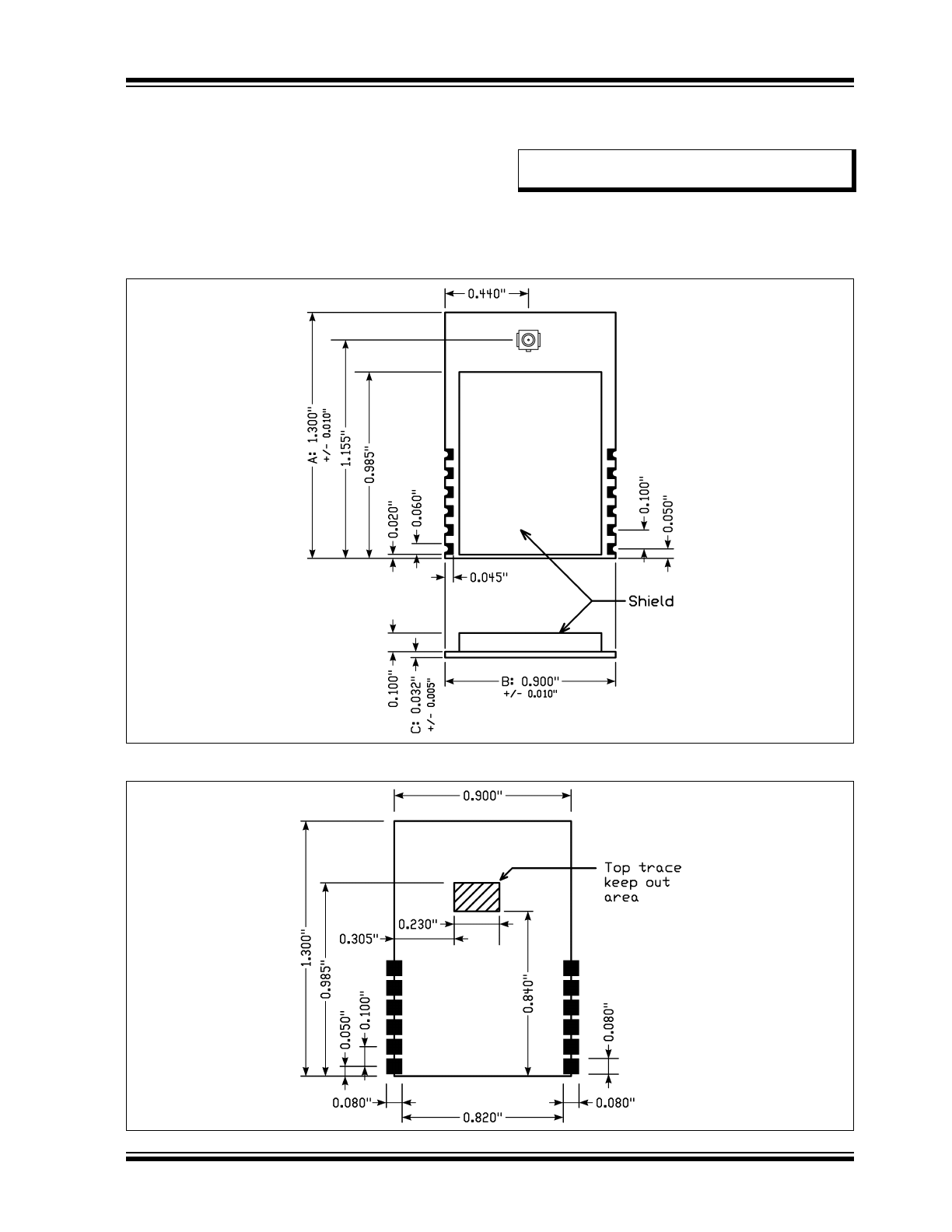
Mounting Details
The MRF24J40MC is a surface mountable module.
Module dimensions are shown in
Figure 1-3
. The
module Printed Circuit Board (PCB) is 0.032" thick
with castellated mounting points on the edge.
Figure 1-4
is a recommended host PCB footprint for
the MRF24J40MC .
The MRF24J40MC has 50Ω ultra miniature coaxial
(U.FL) connector.
FIGURE 1-3:
MODULE DETAILS
FIGURE 1-4:
RECOMMENDED PCB FOOTPRINT
Caution: The U.FL connector is fragile and can only
tolerate very limited number of insertions.
MRF24J40MC
DS75002A-page 8
Preliminary
© 2011 Microchip Technology Inc.
1.3
Operation
The MRF24J40MC module is based on the Microchip
Technology MRF24J40 2.4 GHz IEEE 802.15.4 RF
Transceiver IC. Serial communication and
configuration are documented in the “MRF24J40 Data
Sheet” (DS39776).
This section emphasizes operational settings that are
unique to the MRF24J40MC module design that must
be followed for proper operation.
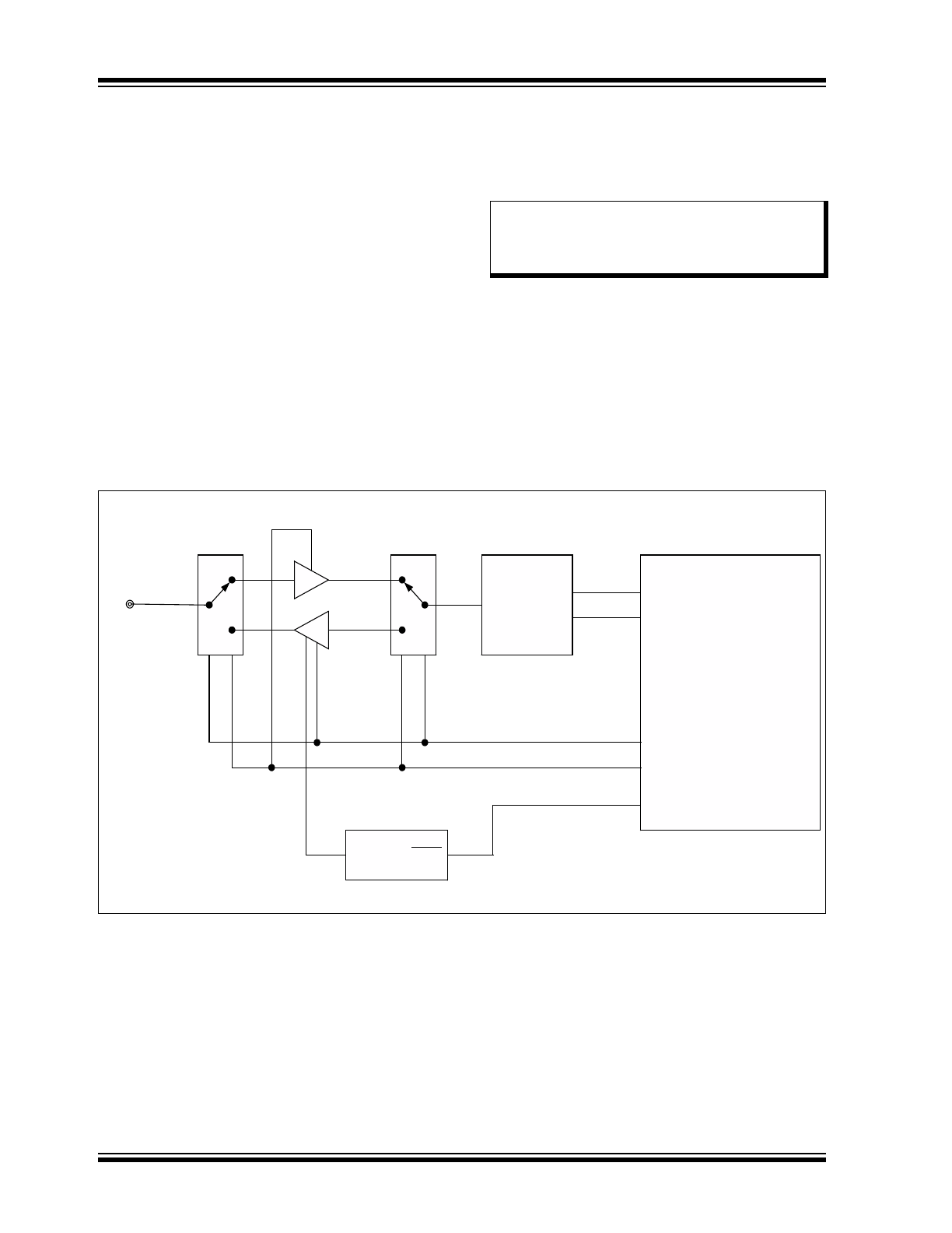
1.3.1
PA/LNA CONTROL
Operation of the PA U3 and LNA U2 is controlled by the
MRF24J40 internal RF state machine through RF
switches, U1 and U4, and the GPIO1 and GPIO2 pins on
the MRF24J40.
Figure 1-5
shows the PA/LNA block
diagram.
Figure 2-2
is the schematic diagram for the
module.
The internal RF state machine is configured for the PA/
LNA Mode by setting TESTMODE (0x22<2:0>) = 111.
Pins GPIO1 and GPIO2 control the RF switches, PA
and LNA automatically when the MRF24J40 receives
and transmits data.
Voltage regulator U5 supplies a regulated 2.2V to the
PA. This provides a stable voltage to the PA over the V
IN
voltage range of the module. U5 is enabled or shutdown
from GPIO3. Ensure that the GPIO3 direction has been
set to output (TRISGP3 (0x34<3>) = 1). Setting a logic
high (GPIO3(0x33<3>) = 1) enables the voltage
regulator and supplies voltage to the PA. Setting a logic
low (GPIO3 (0x33<3>) = 0) will shutdown the voltage
regulator, disabling the PA, and provides the lowest
shutdown current.
FIGURE 1-5:
PA/LNA BLOCK DIAGRAM
Note:
A complete explanation of the operation of
the PA/LNA control is documented in the
“MRF24J40 Data Sheet” (DS39776),
Section 4.2 “External PA/LNA Control”.
MRF24J40
GPIO1
GPIO2
U.FL
Connector
Balun
RFP
RFN
PA
uPG2250T5N
LNA
PA
RF Switch
UPG2179TB
RF Switch
UPG2179TB
LNA
uPC8233TK
V2 V1
V2 V1
GPIO3
Voltage Regulator
TC1187VCT713
V
OUT
SHDN
50
ohm

© 2011 Microchip Technology Inc.
Preliminary
DS75002A-page 9
MRF24J40MC
1.3.2
ENERGY DETECTION (ED)
Before performing an energy detection (see Section
3.6.1 “RSSI Firmware Request (RSSI Mode 1)” in the
“MRF24J40 Data Sheet” (DS39776)), perform the
following steps:
1.
Configure the internal RF state machine to normal
operation (TESTMODE (0x22F<2:0>) = 000).
2.
Configure GPIO2 and GPIO1 direction for
output (TRISGP2 (0x34<2>) = 1 and TRISGP1
(0x34<1>) = 1).
3.
Set GPIO2 (0x33<2>) = 1 and GPIO1
(0x32<1>) = 0. This enables the LNA and
disables the PA.
4.
Perform the energy detection following the steps
in Section 3.6.1 “RSSI Firmware Request (RSSI
Mode 1)” in the “MRF24J40 Data Sheet”
(DS39776).
1.3.3
SLEEP
To get the lowest power consumption from the
MRF24J40MC module during Sleep, it is necessary to
disable the PA, PA voltage regulator and LNA. To do
this, perform the following steps:
1.
Configure the internal RF state machine to normal
operation (TESTMODE (0x22F<2:0>) = 000).
2.
Configure the GPIO3, GPIO2 and GPIO1
direction for output (TRISGP3 (0x34<3>) = 1,
TRISGP2 (0x34<2>) = 1 and TRISGP1
(0x34<1>) = 1).
3.
Set GPIO2 (0x33<2>) = 0 and GPIO1 (0x32<1>)
= 0. This disables the LNA and the PA.
4.
Set GPIO3 (0x33<3>) = 0. This shuts down the
voltage regulator U5 that supplies 2.2 volts to
the PA.
5.
Put the MRF24J40 to Sleep following the steps
in the “MRF24J40 Data Sheet” (DS39776).
When waking the module, re-enable the PA/LNA Mode.
Note:
The LNA will amplify the received signal.
The RSSI value will include the receive
signal strength plus the LNA amplification.
MRF24J40MC
DS75002A-page 10
Preliminary
© 2011 Microchip Technology Inc.
1.3.4
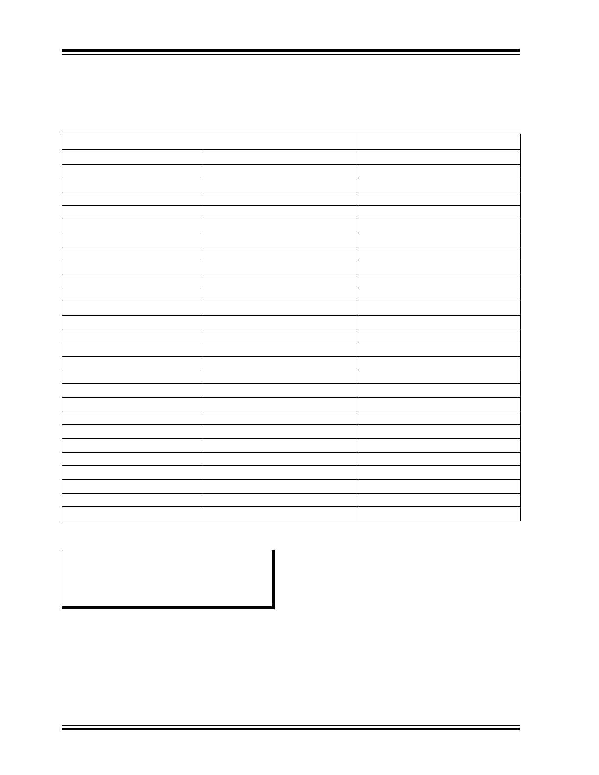
TRANSMIT POWER SETTINGS
Table 1-2
lists the power settings in register RFCON3
(0x203<7:3>) and the output power at antenna
connector J1.
Note 1: Typical output power at antenna connector J1, Channel 11, 50Ω impedance.
TABLE 1-2:
TRANSMIT POWER SETTINGS
RFCON3 (0x203<7:3>)
MRF24J40 Power Setting
Output Power
(1)
(dBm)
11111
–36.3
–26.4
11110
–34.9
–25.2
11101
–33.7
–24.1
11100
–32.8
–23.4
11011
–31.9
–22.7
11010
–31.2
–22.4
11001
–30.5
–21.9
11000
–30.0
–21.6
10111
–26.3
–15.7
10110
–24.9
–14.5
10101
–23.7
–13.7
10100
–22.8
–12.9
10011
–21.9
–12.3
10010
–21.2
–11.8
10001
–20.5
–11.5
10000
–20.0
–11.1
01111
–16.3
–6.6
01110
–14.9
–5.5
01101
–13.7
–4.7
01100
–12.8
–4.0
01011
–11.9
–3.4
01010
–11.2
–2.9
01001
–10.5
–2.5
01000
–10.0
–2.0
00111
–6.3
10.7
00110
–4.9
18.0
00101
–3.7
18.5
Note:
Refer to
Section 3.0 “Regulatory
Approval”
for the required maximum
power setting necessary to maintain
certification requirements for each country
the module will be used.