

2017 Microchip Technology Inc.
DS20005829A-page 1
MIC8115
Features
• Precision Voltage Monitor for 3.3V Power
Supplies
• Specifically Tailored to the AMD Elan SC500
Series
• /RESET Remains Valid with V
CC
as Low as 1.4V
• <15 µA Supply Current
• 1100 ms Minimum Reset Pulse Width
• Manual Reset Input
• Available in 4-Pin SOT-143 Package
Applications
• Portable Equipment
• Intelligent Instruments
• Critical Microprocessor Power Monitoring
• Printers/Computers
• Embedded Controllers
General Description
The MIC8115 is an inexpensive microprocessor
supervisory circuit that monitors power supplies in
microprocessor-based systems.
The function of the MIC8115 is to assert a reset if the
power supply drops below a designated reset threshold
level or if /MR is forced low.
The MIC8115 has an active-low /RESET output. The
reset output is guaranteed to remain asserted for a
minimum of 1100 ms after V
CC
has risen above the
designated reset threshold level. The MIC8115 comes
in a 4-pin SOT-143 package.
Package Type
MIC8115
4-Lead SOT-143 (TU)
GND
/RESET
VCC
/MR
MIC8115
1
2
4
3
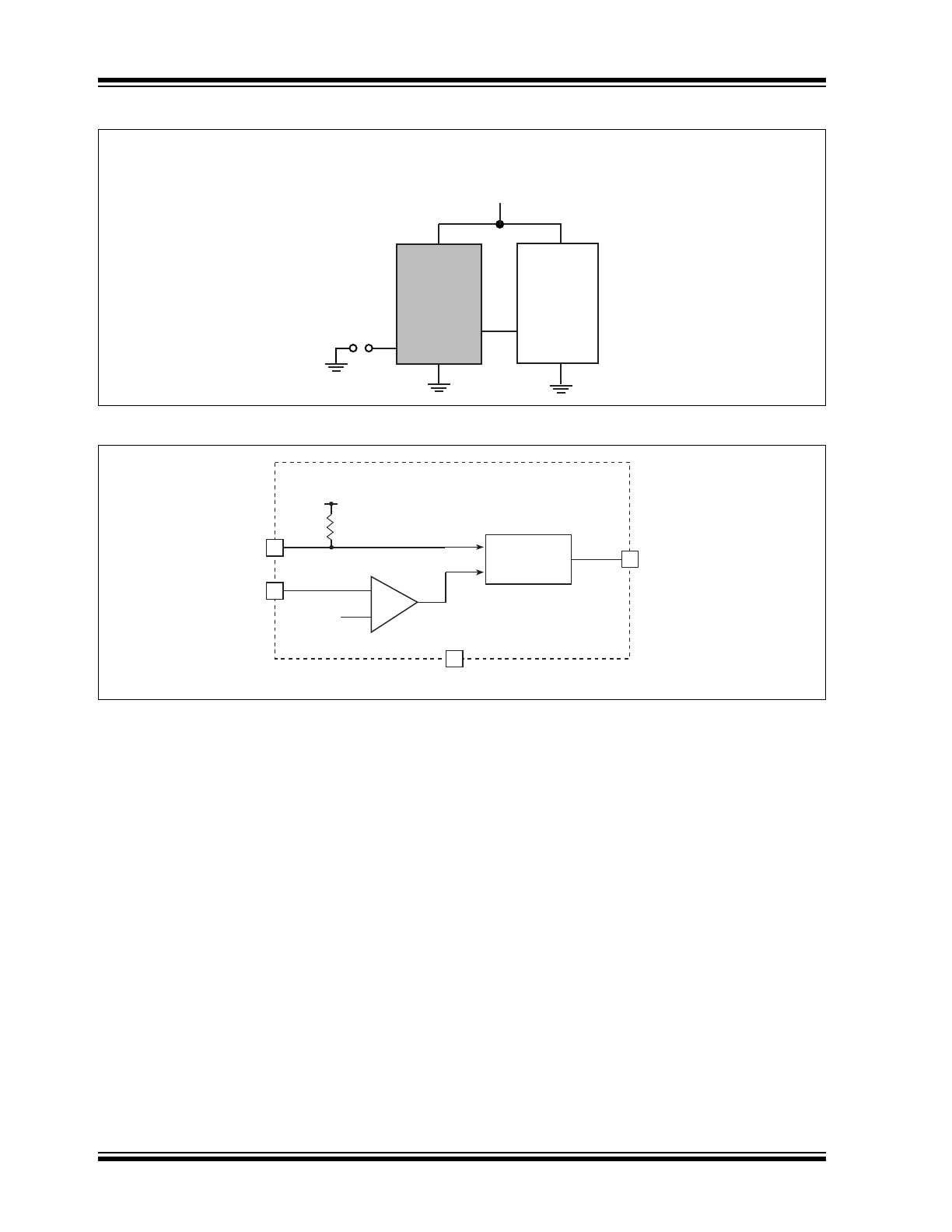
Microprocessor Reset Circuit
MIC8115
DS20005829A-page 2
2017 Microchip Technology Inc.
Typical Application Circuit
Functional Block Diagram
MIC8115
SOT-143
V
CC
MIC8115
μP
/MR
/RESET
V
CC
GND
V
CC
/RESET
+
-
RESET
THRESHOLD (V)
V
CC
(4)
/RESET (2)
GND (1)
RESET
GENERATOR
/MR (3)
V
CC
2017 Microchip Technology Inc.
DS20005829A-page 3
MIC8115
1.0
ELECTRICAL CHARACTERISTICS
Absolute Maximum Ratings †
Terminal Voltage
(V
CC
) ......................................................................................................................................................... –0.3V to +6.0V
(/MR) ...................................................................................................................................................–0.3V to V
CC
+0.3V
Input Current (V
CC
, /MR).........................................................................................................................................20 mA
Output Current (/RESET) ........................................................................................................................................20 mA
Rate of Rise (V
CC
) .............................................................................................................................................. 100 V/µs
ESD Rating,
Note 1
.................................................................................................................................................... 3 kV
Operating Ratings ‡
Power Dissipation (T
A
= +70°C)...........................................................................................................................320 mW
†
Notice: Stresses above those listed under “Absolute Maximum Ratings” may cause permanent damage to the device.
This is a stress rating only and functional operation of the device at those or any other conditions above those indicated
in the operational sections of this specification is not intended. Exposure to maximum rating conditions for extended
periods may affect device reliability.
‡ Notice:
The device is not guaranteed to function outside its operating ratings.
Note 1:
Devices are ESD sensitive. Handling precautions are recommended. Human body model, 1.5 kΩ in series
with 100 pF.
TABLE 1-1:
ELECTRICAL CHARACTERISTICS
Electrical Characteristics:
For typical values, V
CC
= 3.3V; T
A
= +25°C, bold values indicate –40°C ≤ T
A
≤ +85°C,
unless noted.
Parameter
Symbol
Min.
Typ.
Max.
Units
Conditions
Operating Voltage Range
V
CC
1
—
5.5
V
T
A
= –40°C to +85°C
Supply Current
I
CC
—
5
15
µA
—
Reset Voltage Threshold
V
TH
3.00
3.08
3.15
V
—
Reset Timeout Period
t
RST
1100
1700
2500
ms
—
/RESET Output Voltage
V
OH
0.8 x
V
CC
—
—
V
I
SOURCE
= 500 µA
/RESET Output Voltage
V
OL
—
—
0.3
V
V
CC
= V
TH(MIN)
, I
SINK
= 1.2 mA
—
—
0.3
V
CC
= 1V, I
SINK
= 50 µA,
T
A
= –40°C to +85°C
/MR Minimum Pulse Width
—
10
—
—
µs
—
/MR to Reset Delay
—
—
0.5
—
µs
—
/MR Input Threshold
V
IH
0.7 x
V
CC
—
—
V
—
V
IL
—
—
0.25 x
V
CC
—
/MR Pull-Up Resistance
—
10
20
30
kΩ
—
/MR Glitch Immunity
—
—
100
—
ns
—
MIC8115
DS20005829A-page 4
2017 Microchip Technology Inc.
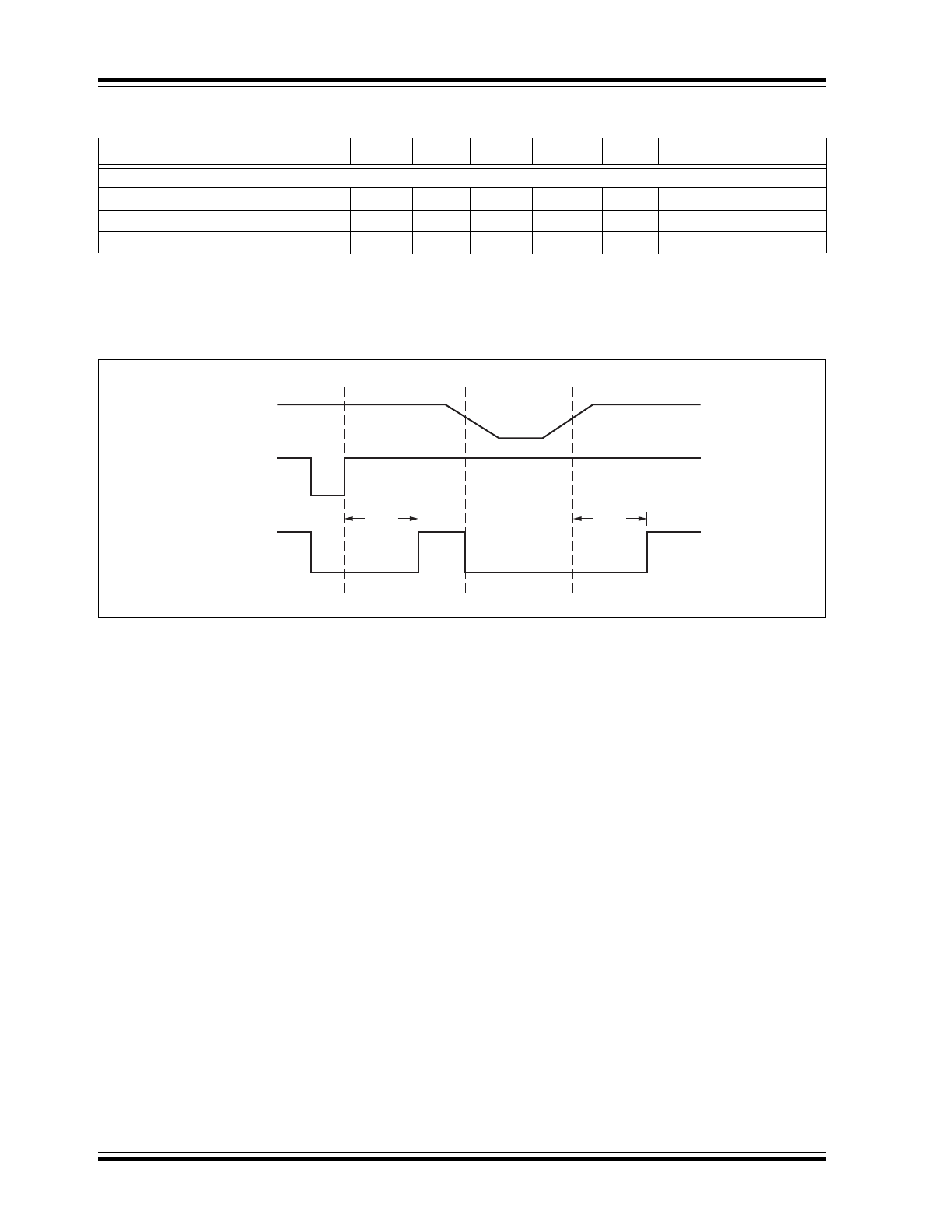
FIGURE 1-1:
Timing Diagram.
TEMPERATURE SPECIFICATIONS (
Note 1
)
Parameters
Sym.
Min.
Typ.
Max.
Units
Conditions
Temperature Ranges
Operating Temperature Range
—
–40
—
+85
°C
—
Storage Temperature Range
T
S
–65
—
+150
°C
—
Lead Temperature
—
—
—
+300
°C
Soldering, 10s
Note 1:
The maximum allowable power dissipation is a function of ambient temperature, the maximum allowable
junction temperature and the thermal resistance from junction to air (i.e., T
A
, T
J
,
JA
). Exceeding the
maximum allowable power dissipation will cause the device operating junction temperature to exceed the
maximum +85°C rating. Sustained junction temperatures above +85°C can impact the device reliability.
V
CC
/MR
/RESET
t
RST
t
RST
V
TH

2017 Microchip Technology Inc.
DS20005829A-page 5
MIC8115
2.0
PIN DESCRIPTIONS
The descriptions of the pins are listed in
Table 2-1
.
TABLE 2-1:
PIN FUNCTION TABLE
Pin Number
Pin Name
Description
1
GND
IC Ground Pin.
2
/RESET
/RESET goes low if either V
CC
falls below the supply reset threshold voltage or if /MR
is asserted. /RESET remains asserted for one reset timeout period 1100 ms
(minimum) after both V
CC
exceeds the supply reset threshold voltage and /MR is
de-asserted.
3
/MR
Manual Reset Input. A logic-low on /MR forces a reset. The reset will remain asserted
as long as /MR is held low and for one reset timeout period (1100 ms, minimum) after
/MR goes high. This input can be shorted to ground via a switch or driven from CMOS
or TTL logic. Pulled high internally through a 20 kΩ resistor. Float if unused.
4
VCC
Power Supply Input.
MIC8115
DS20005829A-page 6
2017 Microchip Technology Inc.
3.0
APPLICATION INFORMATION
3.1
Microprocessor Reset
The /RESET pin is asserted whenever V
CC
falls below
the reset threshold voltage. The reset pin remains
asserted for a period of 1100 ms after V
CC
has risen
above the reset threshold voltage. The reset function
ensures the microprocessor is properly reset and
powers up into a known condition after a power failure.
/RESET will remain valid with V
CC
as low as 1.4V.
3.2
VCC Transients
The MIC8115 is relatively immune to the
negative-going V
CC
glitches below the reset threshold.
Typically, a negative-going transient 125 mV belt the
reset threshold with duration of 20 µs or less will not
cause a reset.
3.3
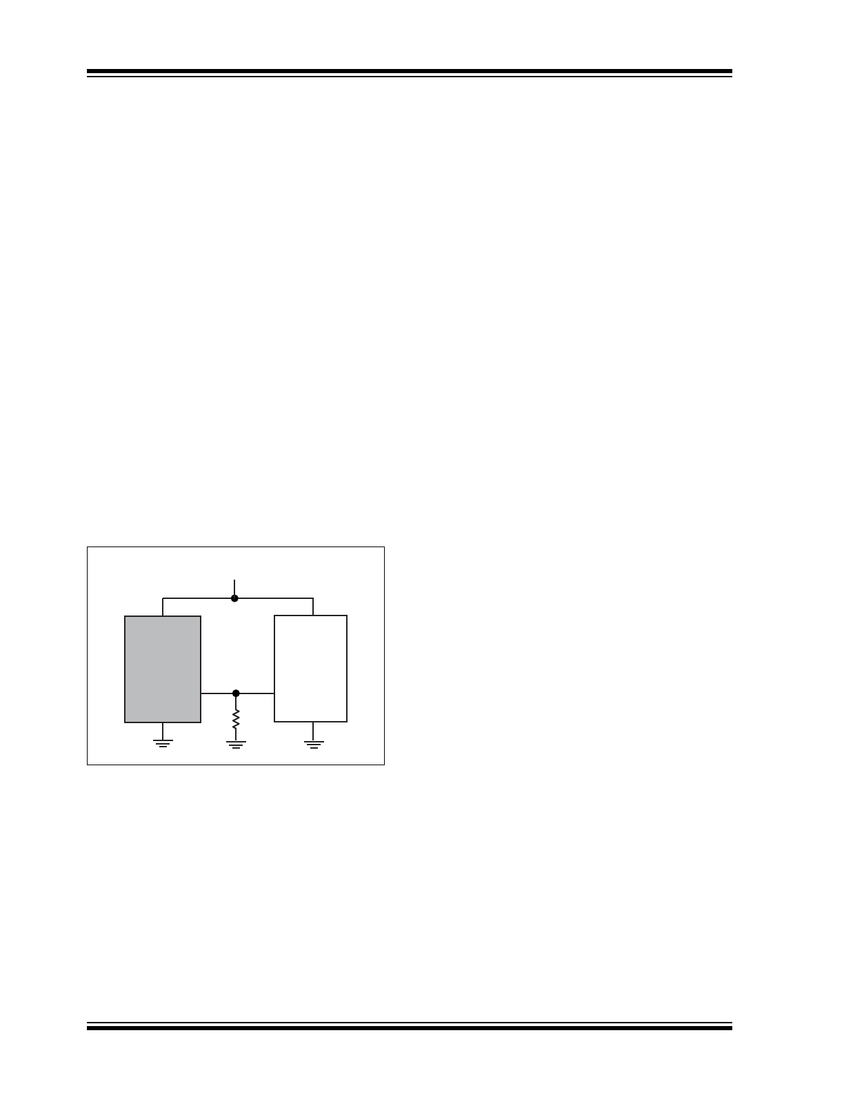
/RESET Valid at Low Voltage
A resistor can be added from the /RESET pin to the
ground to ensure the /RESET output remains low with
V
CC
down to 0V. A 100 kΩ resistor connected from
/RESET to ground is recommended. The resistor
should be large enough not to load the /RESET output
and small enough to pull-down any stray leakage
currents.
FIGURE 3-1:
/RESET Valid to V
CC
= 0V.
V
CC
MIC8115
μP
/RESET
V
CC
GND
V
CC
/RESET
100k
2017 Microchip Technology Inc.
DS20005829A-page 7
MIC8115
4.0
PACKAGING INFORMATION
4.1
Package Marking Information
Example
MNNN
XX
4-Pin SOT-143*
6102
NT
Legend:
XX...X
Product code or customer-specific information
Y
Year code (last digit of calendar year)
YY
Year code (last 2 digits of calendar year)
WW
Week code (week of January 1 is week ‘01’)
NNN
Alphanumeric traceability code
Pb-free JEDEC
®
designator for Matte Tin (Sn)
*
This package is Pb-free. The Pb-free JEDEC designator ( )
can be found on the outer packaging for this package.
●, ▲, ▼ Pin one index is identified by a dot, delta up, or delta down (triangle
mark).
Note
:
In the event the full Microchip part number cannot be marked on one line, it will
be carried over to the next line, thus limiting the number of available
characters for customer-specific information. Package may or may not include
the corporate logo.
Underbar (_) and/or Overbar (⎯) symbol may not be to scale.
3
e
3
e
MIC8115
DS20005829A-page 8
2017 Microchip Technology Inc.
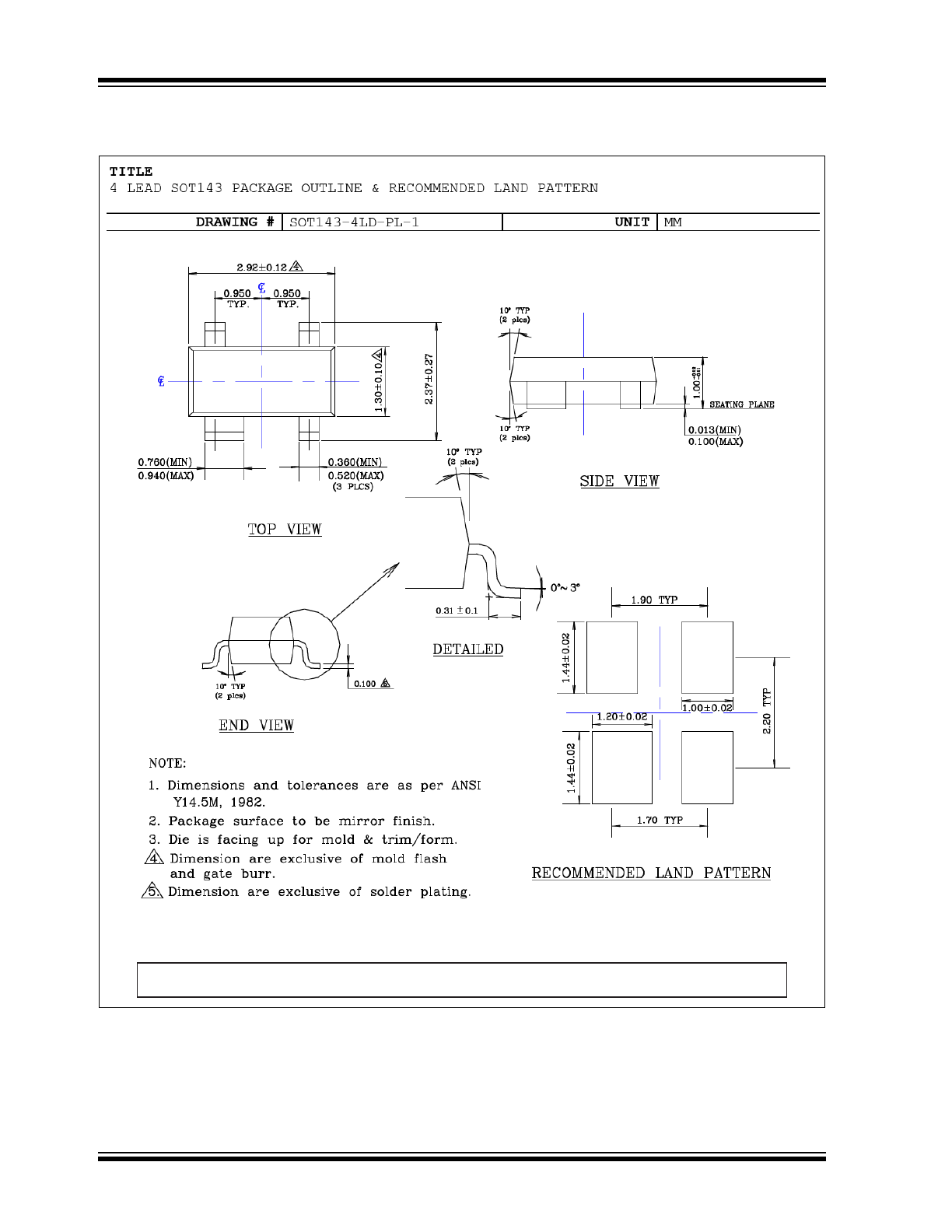
4-Lead SOT-143 Package Outline and Recommended Land Pattern
Note: For the most current package drawings, please see the Microchip Packaging Specification located at
http://www.microchip.com/packaging.

2017 Microchip Technology Inc.
DS20005829A-page 15
MIC8115
APPENDIX A:
REVISION HISTORY
Revision A (August 2017)
• Converted Micrel document MIC8115 to Microchip
data sheet DS20005829A.
• Minor text changes throughout.
• Corrected a pin numbering error in the
Package
Type
image.

MIC8115
DS20005829A-page 16
2017 Microchip Technology Inc.