
2001 Microchip Technology Inc.
DS11184D-page 1
MCP120/130
FEATURES
• Holds microcontroller in reset until supply voltage
reaches stable operating level
• Resets microcontroller during power loss
• Precision monitoring of 3V, 3.3V and 5V systems
• 7 voltage trip points available
• Active low RESET pin
• Open drain output
• Internal pull-up resistor (5 k
Ω
) for MCP130
• Holds RESET for 350 ms (typical)
• RESET to V
CC
= 1.0V
• Accuracy of ±125 mV for 5V systems and ±75 mV
for 3V systems over temperature
• 45
µ
A typical operating current
• Temperature range:
- Industrial (I): -40
°
C to +85
°
C
DESCRIPTION
The Microchip Technology Inc. MCP120/130 is a volt-
age supervisory device designed to keep a microcon-
troller in reset until the system voltage has reached the
proper level and stabilized. It also operates as protec-
tion from brown-out conditions when the supply voltage
drops below a safe operating level. Both devices are
available with a choice of seven different trip voltages
and both have open drain outputs. The MCP130 has an
internal 5 k
Ω
pullup resistor. Both devices have active
low RESET pins. The MCP120/130 will assert the
RESET signal whenever the voltage on the V
DD
pin is
below the trip-point voltage.
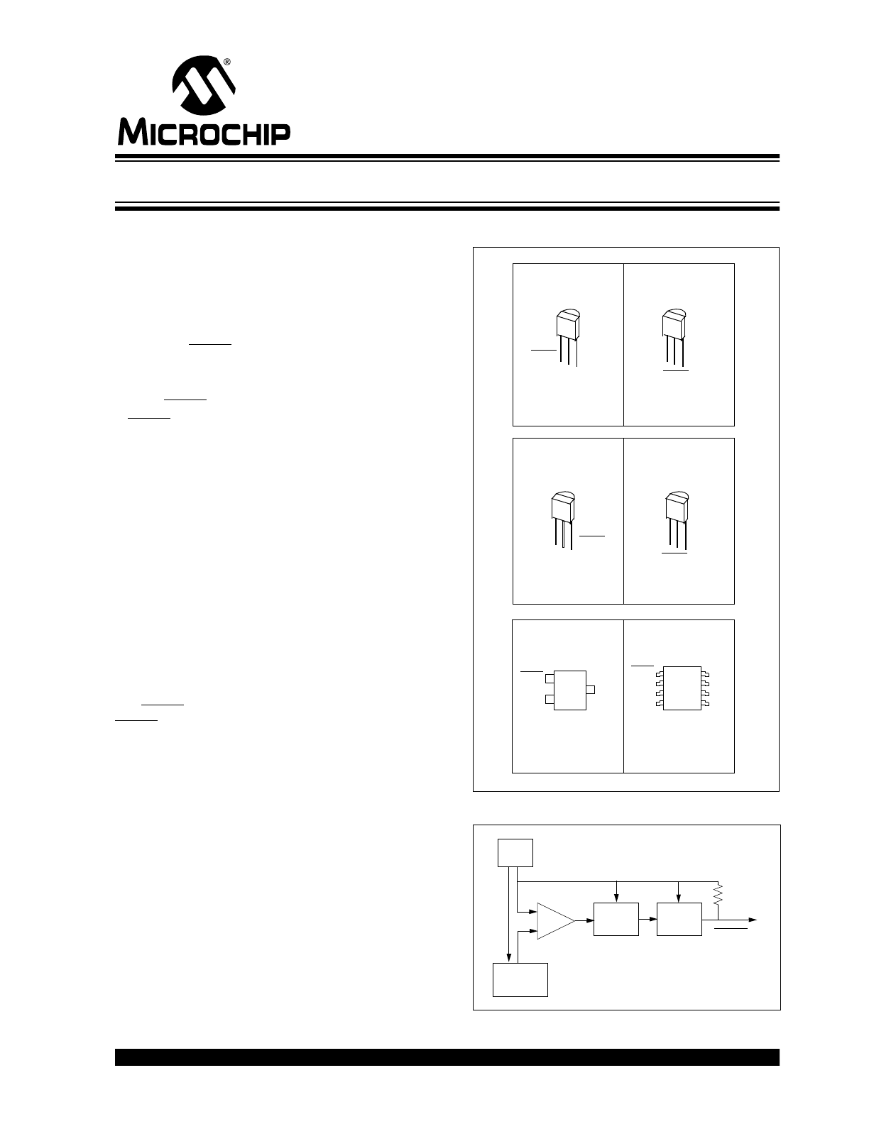
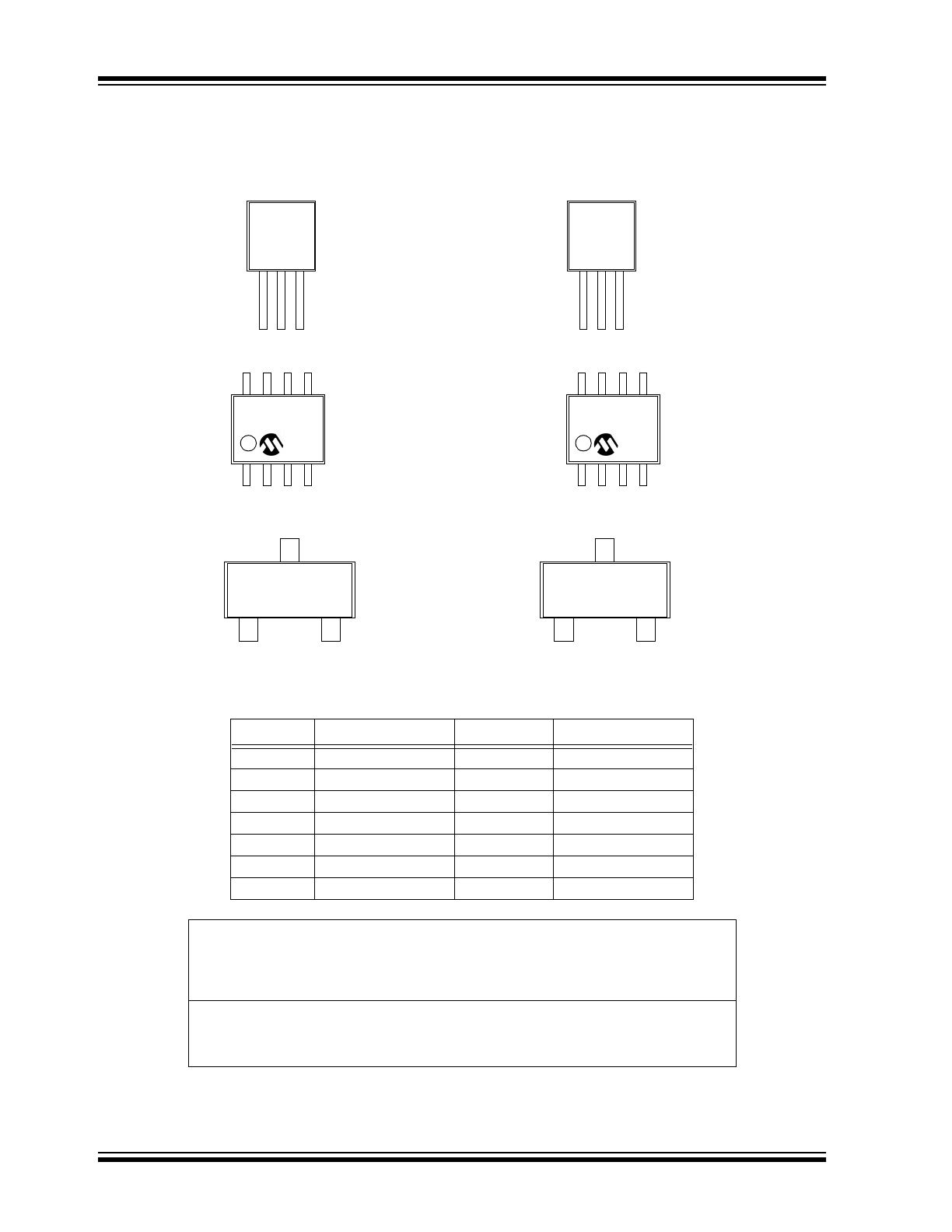
PACKAGES
BLOCK DIAGRAM
V
SS
V
DD
RST
V
SS
V
DD
V
SS
V
DD
RST
V
SS
V
DD
RST
V
SS
RST
V
DD
TO-92 with
‘D’ Bondout
TO-92 WITH
‘F’ BONDOUT
TO-92 with
‘G’ Bondout
TO-92 with
‘H’ Bondout
SOT-23-3
MCP120
MCP130
MCP130
MCP120
MCP130
MCP120
MCP120
MCP130
RST
V
DD
NC
V
SS
1
2
3
4
8
7
6
5
NC
NC
NC
NC
150mil SOIC
MCP120
MCP130
RST
Delay
Circuit
Output
Driver
RESET
V
DD
+
-
Comparator
pull-up on
MCP130
5k
Ω
internal
Bandgap
Reference
only
Microcontroller Supervisory Circuit with Open Drain Output
2001 Microchip Technology Inc.
DS11184D-page 2
MCP120/130
1.0
ELECTRICAL CHARACTERISTICS
1.1
Maximum Ratings*
V
DD
........................................................................ 7.0V
All inputs and outputs w.r.t. V
SS
.....-0.6V to V
DD
+1.0V
Storage temperature .......................... -65°C to +150°C
Ambient temp. with power applied ..... -65°C to +125°C
ESD protection on all pins
..................................... ≥
2 kV
*Notice: Stresses above those listed under “Maximum
Ratings” may cause permanent damage to the device.
This is a stress rating only and functional operation of
the device at those or any other conditions above those
indicated in the operational listings of this specification
is not implied. Exposure to maximum rating conditions
for extended periods may affect device reliability.
DC AND AC CHARACTERISTICS
All parameters apply at the
specified temp and voltage
ranges unless otherwise noted.
V
DD
= 1.0 - 5.5V
Industrial (I): -40°C to +85°C
Parameter
Symbol
Min.
Typ.
Max.
Units
Test Conditions
Operating Voltage Range
V
DD
1.0
—
5.5
V
V
DD
Value to RESET
V
DD
MIN
1.0
—
—
V
Operating Current
I
DD
—
45
60
µ
A
V
DD
= 5.5V (no load)
V
DD
Trip Point
MCP1X0-270
MCP1X0-300
MCP1X0-315
MCP1X0-450
MCP1X0-460
MCP1X0-475
MCP1X0-485
V
TRIP
2.55
2.85
3.0
4.25
4.35
4.50
4.60
2.625
2.925
3.075
4.375
4.475
4.625
4.725
2.7
3.0
3.15
4.50
4.60
4.75
4.85
V
RESET Low
Level Output
Voltage
MCP1X0-270
MCP1X0-300
MCP1X0-315
V
OL
—
—
0.4
V
I
OL
= 3.2 mA,
V
DD
= V
TRIP
MIN
MCP1X0-450
MCP1X0-460
MCP1X0-475
MCP1X0-485
—
—
0.6
I
OL
= 8.5 mA,
V
DD
= V
TRIP
MIN
RESET High
Level Output
Voltage
(MCP130 Only)
MCP130-xxx
(All V
TRIP
Points)
V
OH
V
DD
-0.7
—
—
V
I
OH
= 50
µ
A,V
DD
> V
TRIP
MAX
Pull-up Resistor (MCP130 Only)
—
5
—
k
Ω
Output Leakage (MCP120 Only)
—
1
—
µ
A
Threshold Hysteresis
V
HYS
—
50
—
mV
V
DD
Detect to RESET Inactive
t
RPU
150
350
700
ms
V
DD
Detect to RESET
t
RPD
—
10
—
µ
s
V
DD
ramped from V
TRIP
MAX
+
250 mV
down to V
TRIP
MIN
-
250 mV
Note:
Typical values are for 25°C and V
DD
= 5.0V
2001 Microchip Technology Inc.
DS11184D-page 3
MCP120/130
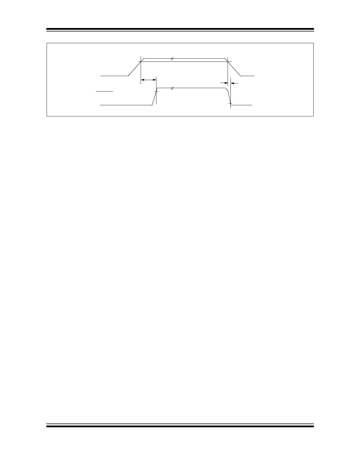
Figure 1-1:
MCP120/130 Timing Diagram
V
DD
RESET
V
OH
t
RPU
V
TRIP
t
RPD
V
OH
MCP120/130
DS11184D-page 4
2001 Microchip Technology Inc.
2.0
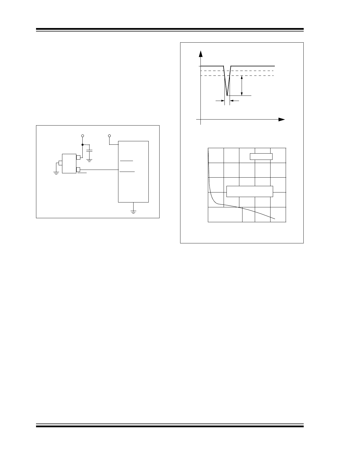
APPLICATIONS INFORMATION
2.1
The Need for Supervisory Circuits
For many of today’s microcontroller applications, care
must be taken to prevent low power conditions that can
cause many different system problems. The most com-
mon causes are brown-out conditions where the sys-
tem supply drops below the operating level momentar-
ily, and the second, is when a slowly decaying power
supply causes the microcontroller to begin executing
instructions without enough voltage to sustain SRAM
and producing indeterminate results.
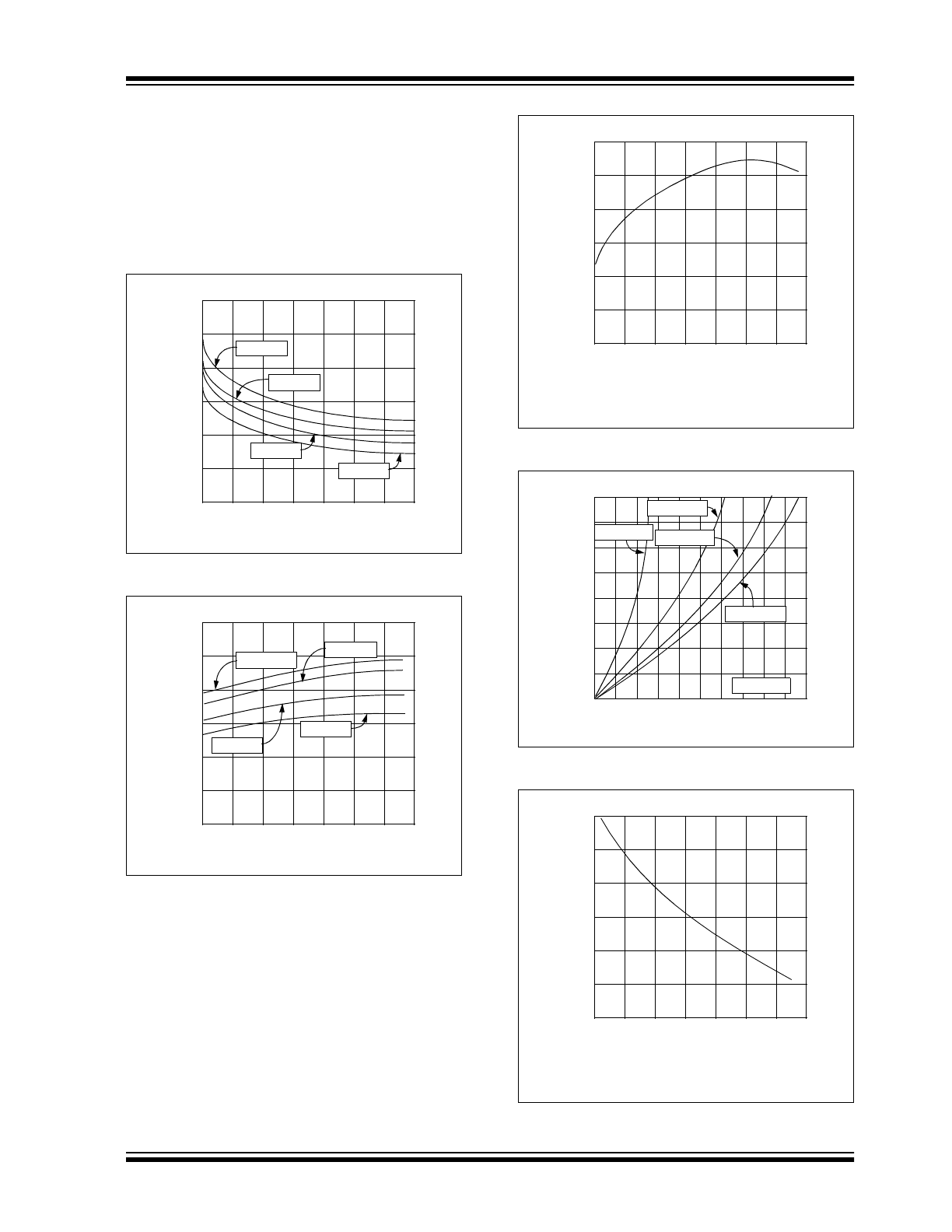
Figure 2-1:
Typical Application
2.2
Negative Going V
DD
Transients
Many system designers implementing POR circuits are
concerned about the minimum pulse width required to
cause a reset. Figure 2-2 shows typical transient
voltage below the trip point (V
TRIP
- V
DD
) vs. transient
duration. It shows that the farther below the trip point
the transient pulse goes, the duration of the pulse
required to cause a reset gets shorter. A 0.1
µ
F bypass
cap mounted as close as possible to the V
DD
pin pro-
vides additional transient immunity.
Figure 2-2:
Typical Transient Response
Microcontroller
MCLR
V
SS
RST
MCP120
or
RESET
V
SS
V
DD
V
DD
Bypass
Capacitor
V
DD
TIME
SUP
P
L
Y
VO
L
T
AG
E
0
0
5V
V
TRIP
MAX
V
TRIP
MIN
Transient
Duration
(V
TRIP
MIN
-
V
DD
)
0
1
2
3
V
TRIP
- V
DD
(V)
10
8
6
4
2
0
T
R
ANS
IENT
DURA
T
ION (
µ
S
)
4
5
T
A
= +25°C
Transients above the
curve will cause a reset
Transients below
the curve will NOT
cause a reset
2001 Microchip Technology Inc.
DS11184D-page 5
MCP120/130
2.3
Effect of Temperature on Timeout
Period (t
RPU
)
The timeout period (t
RPU
) determines how long the
device remains in the reset condition. This is controlled
by an internal RC timer and is effected by both V
DD
and temperature. The graph shown in Figure 2-3
shows typical response for different V
DD
values and
temperatures.
Figure 2-3:
t
RPU
vs. Temperature
Figure 2-4:
I
DD
vs. Temperature
Figure 2-5:
Normalized V
TRIP
vs. Temperature
Figure 2-6:
V
OL
vs. I
OL
Figure 2-7:
Normalized I
OL
vs. Temperature
-40
-20
20
60
TEMPERATURE (°C)
600
500
400
300
200
100
T
IME
OUT
P
E
R
IOD
(t
RP
U
) (
m
s
)
80
100
0
40
700
V
DD
= 5V
V
DD
= 4V
V
DD
= 3V
V
DD
= 6V
-40
-20
20
60
TEMPERATURE (°C)
50
40
30
20
10
0
OPERA
T
IN
G CURRENT
(
µ
A)
80
100
0
40
60
V
DD
= 5V
V
DD
= 3V
V
DD
= 5.5V
V
DD
= 4V
-40
-20
20
60
TEMPERATURE (°C)
1.000
0.998
0.996
0.994
0.992
0.997
NORM
AL
IZ
ED T
HRESHOL
D*
(
V
TR
IP
)
80
100
0
40
1.002
* Multiply value at 25°C by this
factor to determine the value at
temperature
0
2
6
10
500
400
300
200
100
0
V
OL
(m
V
)
12
4
8
600
700
800
14 16 18 20
V
DD
= 3.5V
V
DD
= 1.5V
V
DD
= 4.5V
V
DD
= 2.5V
T
A
= +25°C
I
OL
(mA)
-40
-20
20
60
TEMPERATURE (°C)
1.2
1.1
1.00
0.9
0.8
0.7
NORM
AL
IZ
ED I
OL
*
80
100
0
40
1.3
* Multiply value at 25°C by this
factor to determine the value at
temperature
MCP120/130
DS11184D-page 6
2001 Microchip Technology Inc.
3.0
PACKAGING INFORMATION
3.1
Package Marking Information
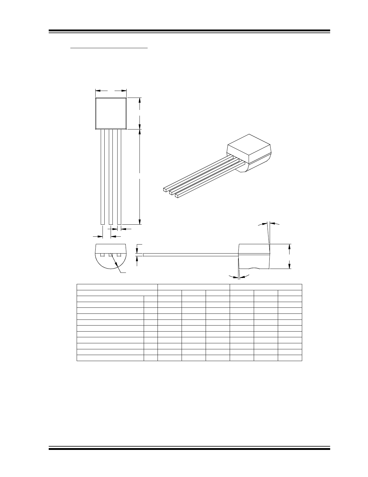
3-Lead Plastic Transistor Outline (TO-92)
Example:
3-Lead Plastic Small Outline Transistor (SOT23)
Example:
Legend: XX...X
Customer specific information*
YY
Year code (last 2 digits of calendar year)
WW
Week code (week of January 1 is week ‘01’)
NNN
Alphanumeric traceability code
Note:
In the event the full Microchip part number cannot be marked on one line, it will
be carried over to the next line thus limiting the number of available characters
for customer specific information.
*
Standard OTP marking consists of Microchip part number, year code, week code, and traceability code.
For OTP marking beyond this, certain price adders apply. Please check with your Microchip Sales Office.
For QTP devices, any special marking adders are included in QTP price.
XXXXXX
XXXXXX
XXXXXX
YWWNNN
MCP120
XXXXXX
XXXXXX
YWWNNN
XXNN
PKNN
SOT23 PARTS LABELING:
The table below identifies the first 2 characters (XX) in the 4-character field
(XXNN) for marking of the 3-Lead SOT23 package.
Mark
Part Number
Mark
Part Number
SJ
MCP120T-270I/TT
PJ
MCP130T-270I/TT
SK
MCP120T-300I/TT
PK
MCP130T-300I/TT
SL
MCP120T-315I/TT
PL
MCP130T-315I/TT
SM
MCP120T-450I/TT
PM
MCP130T-450I/TT
SN
MCP120T-460I/TT
PN
MCP130T-460I/TT
SO
MCP120T-475I/TT
PO
MCP130T-475I/TT
SP
MCP120T-485I/TT
PP
MCP130T-485I/TT
8-Lead Plastic Small Outline (SOIC)
Example:
XXXXYYWW
NNN
XXXXXXXX
XXXXYYWW
NNN
MCP120
2001 Microchip Technology Inc.
DS11184D-page 7
MCP120/130
3.2
Package Detail Information
3-Lead Plastic Transistor Outline (TO) (TO-92)
4
3
2
4
3
2
β
Mold Draft Angle Bottom
6
5
4
6
5
4
α
0.56
0.48
0.41
.022
.019
.016
B
Lead Width
0.51
0.43
0.36
.020
.017
.014
c
Lead Thickness
2.41
2.29
2.16
.095
.090
.085
R
Molded Package Radius
4.95
4.64
4.32
.195
.183
.170
D
Overall Length
4.95
4.71
4.45
.195
.186
.175
E1
Overall Width
3.94
3.62
3.30
.155
.143
.130
A
Bottom to Package Flat
1.27
.050
p
Pitch
3
3
n
Number of Pins
MAX
NOM
MIN
MAX
NOM
MIN
Dimension Limits
MILLIMETERS
INCHES*
Units
R
n
1
3
α
p
L
B
A
c
β
1
D
2
E1
Tip to Seating Plane
L
.500
.555
.610
12.70
14.10
15.49
*Controlling Parameter
Mold Draft Angle Top
Notes:
Dimensions D and E1 do not include mold flash or protrusions. Mold flash or protrusions shall not exceed
.010” (0.254mm) per side.
JEDEC Equivalent: TO-92
Drawing No. C04-101
MCP120/130
DS11184D-page 8
2001 Microchip Technology Inc.
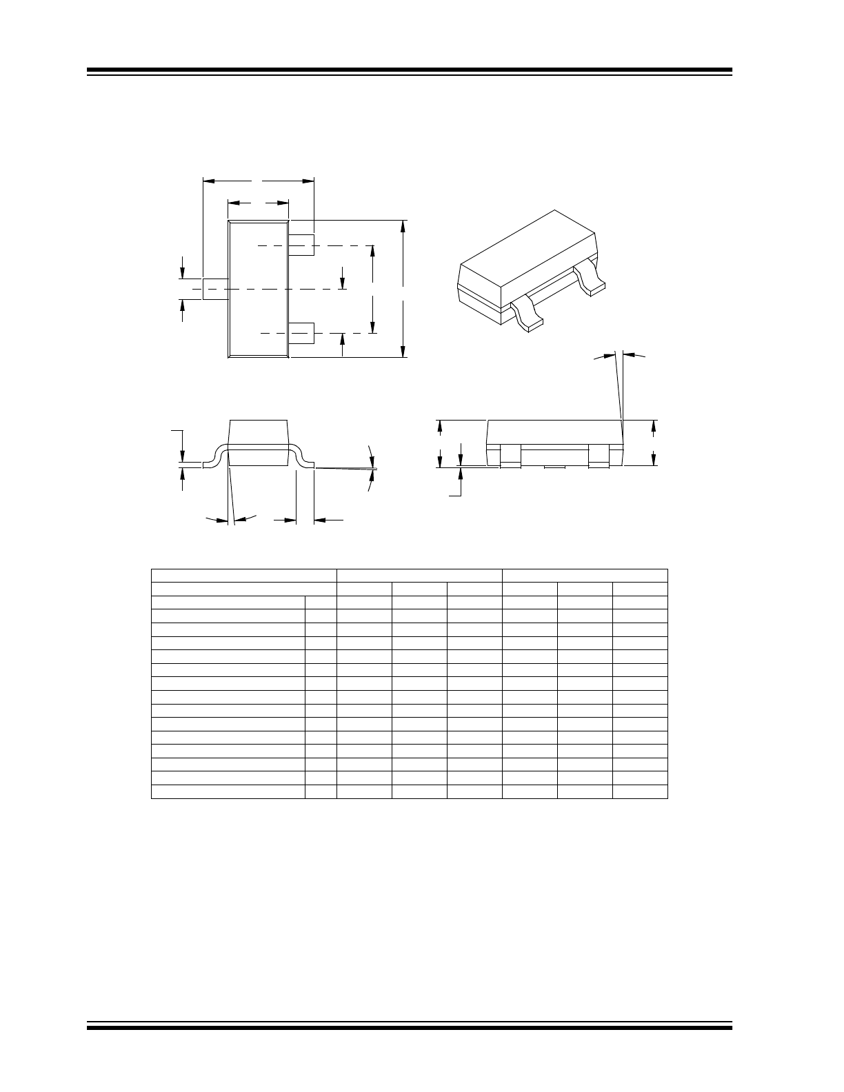
3-Lead Plastic Small Outline Transistor (TT) (SOT23)
10
5
0
10
5
0
β
Mold Draft Angle Bottom
10
5
0
10
5
0
α
Mold Draft Angle Top
0.51
0.44
0.37
.020
.017
.015
B
Lead Width
0.18
0.14
0.09
.007
.006
.004
c
Lead Thickness
10
5
0
10
5
0
φ
Foot Angle
0.55
0.45
0.35
.022
.018
.014
L
Foot Length
3.04
2.92
2.80
.120
.115
.110
D
Overall Length
1.40
1.30
1.20
.055
.051
.047
E1
Molded Package Width
2.64
2.37
2.10
.104
.093
.083
E
Overall Width
0.10
0.06
0.01
.004
.002
.000
A1
Standoff
§
1.02
0.95
0.88
.040
.037
.035
A2
Molded Package Thickness
1.12
1.01
0.89
.044
.040
.035
A
Overall Height
1.92
.076
p1
Outside lead pitch (basic)
0.96
.038
p
Pitch
3
3
n
Number of Pins
MAX
NOM
MIN
MAX
NOM
MIN
Dimension Limits
MILLIMETERS
INCHES*
Units
2
1
p
D
B
n
E
E1
L
c
β
φ
α
A2
A
A1
p1
* Controlling Parameter
Notes:
Dimensions D and E1 do not include mold flash or protrusions. Mold flash or protrusions shall not exceed
.010” (0.254mm) per side.
JEDEC Equivalent: TO-236
Drawing No. C04-104
§ Significant Characteristic
2001 Microchip Technology Inc.
DS11184D-page 9
MCP120/130
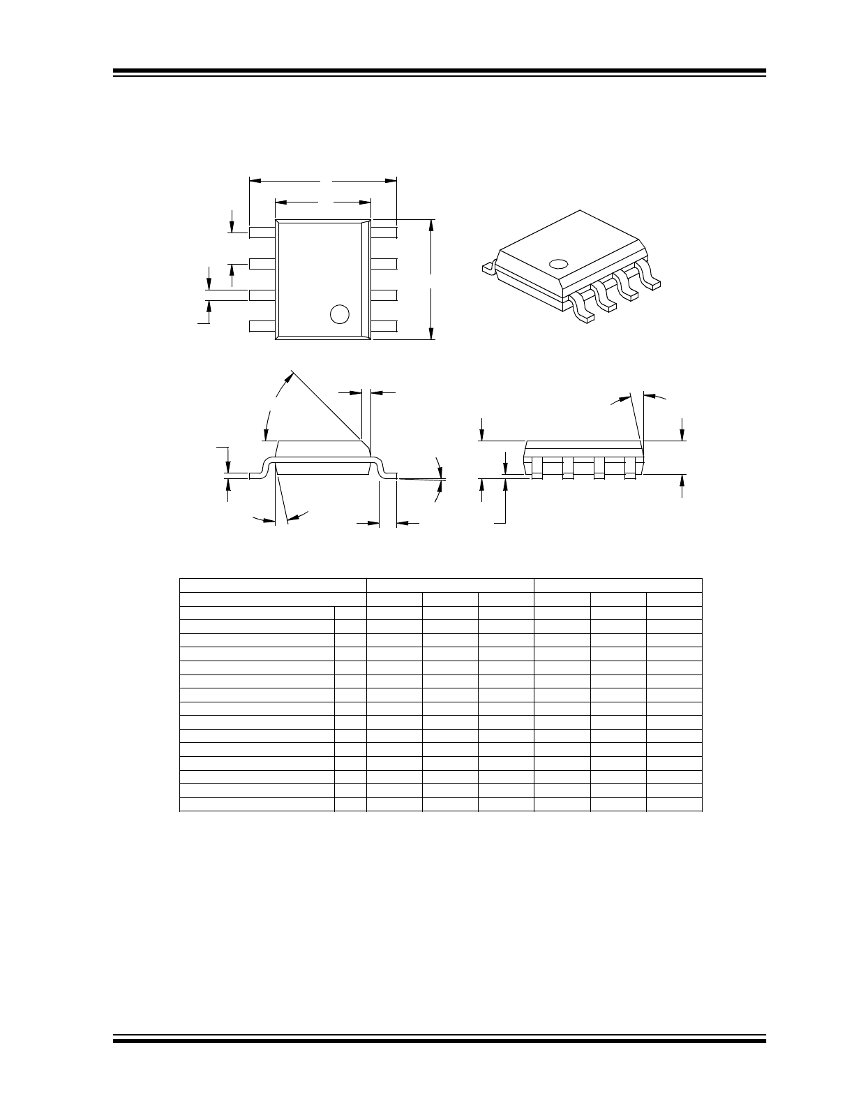
8-Lead Plastic Small Outline (SN) – Narrow, 150 mil (SOIC
Foot Angle
φ
0
4
8
0
4
8
15
12
0
15
12
0
β
Mold Draft Angle Bottom
15
12
0
15
12
0
α
Mold Draft Angle Top
0.51
0.42
0.33
.020
.017
.013
B
Lead Width
0.25
0.23
0.20
.010
.009
.008
c
Lead Thickness
0.76
0.62
0.48
.030
.025
.019
L
Foot Length
0.51
0.38
0.25
.020
.015
.010
h
Chamfer Distance
5.00
4.90
4.80
.197
.193
.189
D
Overall Length
3.99
3.91
3.71
.157
.154
.146
E1
Molded Package Width
6.20
6.02
5.79
.244
.237
.228
E
Overall Width
0.25
0.18
0.10
.010
.007
.004
A1
Standoff
§
1.55
1.42
1.32
.061
.056
.052
A2
Molded Package Thickness
1.75
1.55
1.35
.069
.061
.053
A
Overall Height
1.27
.050
p
Pitch
8
8
n
Number of Pins
MAX
NOM
MIN
MAX
NOM
MIN
Dimension Limits
MILLIMETERS
INCHES*
Units
2
1
D
n
p
B
E
E1
h
L
β
c
45
°
φ
A2
α
A
A1
* Controlling Parameter
Notes:
Dimensions D and E1 do not include mold flash or protrusions. Mold flash or protrusions shall not exceed
.010” (0.254mm) per side.
JEDEC Equivalent: MS-012
Drawing No. C04-057
§ Significant Characteristic

MCP120/130
DS11184D-page 10
2001 Microchip Technology Inc.
ON-LINE SUPPORT
Microchip provides on-line support on the Microchip
World Wide Web (WWW) site.
The web site is used by Microchip as a means to make
files and information easily available to customers. To
view the site, the user must have access to the Internet
and a web browser, such as Netscape or Microsoft
Explorer. Files are also available for FTP download
from our FTP site.
Connecting to the Microchip Internet Web Site
The Microchip web site is available by using your
favorite Internet browser to attach to:
www.microchip.com
The file transfer site is available by using an FTP ser-
vice to connect to:
ftp://ftp.microchip.com
The web site and file transfer site provide a variety of
services. Users may download files for the latest
Development Tools, Data Sheets, Application Notes,
User’s Guides, Articles and Sample Programs. A vari-
ety of Microchip specific business information is also
available, including listings of Microchip sales offices,
distributors and factory representatives. Other data
available for consideration is:
• Latest Microchip Press Releases
• Technical Support Section with Frequently Asked
Questions
• Design Tips
• Device Errata
• Job Postings
• Microchip Consultant Program Member Listing
• Links to other useful web sites related to
Microchip Products
• Conferences for products, Development Systems,
technical information and more
• Listing of seminars and events
Systems Information and Upgrade Hot Line
The Systems Information and Upgrade Line provides
system users a listing of the latest versions of all of
Microchip's development systems software products.
Plus, this line provides information on how customers
can receive any currently available upgrade kits.The
Hot Line Numbers are:
1-800-755-2345 for U.S. and most of Canada, and
1-480-792-7302 for the rest of the world.
2001 Microchip Technology Inc.
DS11184D-page 1
MCP120/130
FEATURES
• Holds microcontroller in reset until supply voltage
reaches stable operating level
• Resets microcontroller during power loss
• Precision monitoring of 3V, 3.3V and 5V systems
• 7 voltage trip points available
• Active low RESET pin
• Open drain output
• Internal pull-up resistor (5 k
Ω
) for MCP130
• Holds RESET for 350 ms (typical)
• RESET to V
CC
= 1.0V
• Accuracy of ±125 mV for 5V systems and ±75 mV
for 3V systems over temperature
• 45
µ
A typical operating current
• Temperature range:
- Industrial (I): -40
°
C to +85
°
C
DESCRIPTION
The Microchip Technology Inc. MCP120/130 is a volt-
age supervisory device designed to keep a microcon-
troller in reset until the system voltage has reached the
proper level and stabilized. It also operates as protec-
tion from brown-out conditions when the supply voltage
drops below a safe operating level. Both devices are
available with a choice of seven different trip voltages
and both have open drain outputs. The MCP130 has an
internal 5 k
Ω
pullup resistor. Both devices have active
low RESET pins. The MCP120/130 will assert the
RESET signal whenever the voltage on the V
DD
pin is
below the trip-point voltage.
PACKAGES
BLOCK DIAGRAM
V
SS
V
DD
RST
V
SS
V
DD
V
SS
V
DD
RST
V
SS
V
DD
RST
V
SS
RST
V
DD
TO-92 with
‘D’ Bondout
TO-92 WITH
‘F’ BONDOUT
TO-92 with
‘G’ Bondout
TO-92 with
‘H’ Bondout
SOT-23-3
MCP120
MCP130
MCP130
MCP120
MCP130
MCP120
MCP120
MCP130
RST
V
DD
NC
V
SS
1
2
3
4
8
7
6
5
NC
NC
NC
NC
150mil SOIC
MCP120
MCP130
RST
Delay
Circuit
Output
Driver
RESET
V
DD
+
-
Comparator
pull-up on
MCP130
5k
Ω
internal
Bandgap
Reference
only
Microcontroller Supervisory Circuit with Open Drain Output
2001 Microchip Technology Inc.
DS11184D-page 2
MCP120/130
1.0
ELECTRICAL CHARACTERISTICS
1.1
Maximum Ratings*
V
DD
........................................................................ 7.0V
All inputs and outputs w.r.t. V
SS
.....-0.6V to V
DD
+1.0V
Storage temperature .......................... -65°C to +150°C
Ambient temp. with power applied ..... -65°C to +125°C
ESD protection on all pins
..................................... ≥
2 kV
*Notice: Stresses above those listed under “Maximum
Ratings” may cause permanent damage to the device.
This is a stress rating only and functional operation of
the device at those or any other conditions above those
indicated in the operational listings of this specification
is not implied. Exposure to maximum rating conditions
for extended periods may affect device reliability.
DC AND AC CHARACTERISTICS
All parameters apply at the
specified temp and voltage
ranges unless otherwise noted.
V
DD
= 1.0 - 5.5V
Industrial (I): -40°C to +85°C
Parameter
Symbol
Min.
Typ.
Max.
Units
Test Conditions
Operating Voltage Range
V
DD
1.0
—
5.5
V
V
DD
Value to RESET
V
DD
MIN
1.0
—
—
V
Operating Current
I
DD
—
45
60
µ
A
V
DD
= 5.5V (no load)
V
DD
Trip Point
MCP1X0-270
MCP1X0-300
MCP1X0-315
MCP1X0-450
MCP1X0-460
MCP1X0-475
MCP1X0-485
V
TRIP
2.55
2.85
3.0
4.25
4.35
4.50
4.60
2.625
2.925
3.075
4.375
4.475
4.625
4.725
2.7
3.0
3.15
4.50
4.60
4.75
4.85
V
RESET Low
Level Output
Voltage
MCP1X0-270
MCP1X0-300
MCP1X0-315
V
OL
—
—
0.4
V
I
OL
= 3.2 mA,
V
DD
= V
TRIP
MIN
MCP1X0-450
MCP1X0-460
MCP1X0-475
MCP1X0-485
—
—
0.6
I
OL
= 8.5 mA,
V
DD
= V
TRIP
MIN
RESET High
Level Output
Voltage
(MCP130 Only)
MCP130-xxx
(All V
TRIP
Points)
V
OH
V
DD
-0.7
—
—
V
I
OH
= 50
µ
A,V
DD
> V
TRIP
MAX
Pull-up Resistor (MCP130 Only)
—
5
—
k
Ω
Output Leakage (MCP120 Only)
—
1
—
µ
A
Threshold Hysteresis
V
HYS
—
50
—
mV
V
DD
Detect to RESET Inactive
t
RPU
150
350
700
ms
V
DD
Detect to RESET
t
RPD
—
10
—
µ
s
V
DD
ramped from V
TRIP
MAX
+
250 mV
down to V
TRIP
MIN
-
250 mV
Note:
Typical values are for 25°C and V
DD
= 5.0V
2001 Microchip Technology Inc.
DS11184D-page 3
MCP120/130
Figure 1-1:
MCP120/130 Timing Diagram
V
DD
RESET
V
OH
t
RPU
V
TRIP
t
RPD
V
OH
MCP120/130
DS11184D-page 4
2001 Microchip Technology Inc.
2.0
APPLICATIONS INFORMATION
2.1
The Need for Supervisory Circuits
For many of today’s microcontroller applications, care
must be taken to prevent low power conditions that can
cause many different system problems. The most com-
mon causes are brown-out conditions where the sys-
tem supply drops below the operating level momentar-
ily, and the second, is when a slowly decaying power
supply causes the microcontroller to begin executing
instructions without enough voltage to sustain SRAM
and producing indeterminate results.
Figure 2-1:
Typical Application
2.2
Negative Going V
DD
Transients
Many system designers implementing POR circuits are
concerned about the minimum pulse width required to
cause a reset. Figure 2-2 shows typical transient
voltage below the trip point (V
TRIP
- V
DD
) vs. transient
duration. It shows that the farther below the trip point
the transient pulse goes, the duration of the pulse
required to cause a reset gets shorter. A 0.1
µ
F bypass
cap mounted as close as possible to the V
DD
pin pro-
vides additional transient immunity.
Figure 2-2:
Typical Transient Response
Microcontroller
MCLR
V
SS
RST
MCP120
or
RESET
V
SS
V
DD
V
DD
Bypass
Capacitor
V
DD
TIME
SUP
P
L
Y
VO
L
T
AG
E
0
0
5V
V
TRIP
MAX
V
TRIP
MIN
Transient
Duration
(V
TRIP
MIN
-
V
DD
)
0
1
2
3
V
TRIP
- V
DD
(V)
10
8
6
4
2
0
T
R
ANS
IENT
DURA
T
ION (
µ
S
)
4
5
T
A
= +25°C
Transients above the
curve will cause a reset
Transients below
the curve will NOT
cause a reset
2001 Microchip Technology Inc.
DS11184D-page 5
MCP120/130
2.3
Effect of Temperature on Timeout
Period (t
RPU
)
The timeout period (t
RPU
) determines how long the
device remains in the reset condition. This is controlled
by an internal RC timer and is effected by both V
DD
and temperature. The graph shown in Figure 2-3
shows typical response for different V
DD
values and
temperatures.
Figure 2-3:
t
RPU
vs. Temperature
Figure 2-4:
I
DD
vs. Temperature
Figure 2-5:
Normalized V
TRIP
vs. Temperature
Figure 2-6:
V
OL
vs. I
OL
Figure 2-7:
Normalized I
OL
vs. Temperature
-40
-20
20
60
TEMPERATURE (°C)
600
500
400
300
200
100
T
IME
OUT
P
E
R
IOD
(t
RP
U
) (
m
s
)
80
100
0
40
700
V
DD
= 5V
V
DD
= 4V
V
DD
= 3V
V
DD
= 6V
-40
-20
20
60
TEMPERATURE (°C)
50
40
30
20
10
0
OPERA
T
IN
G CURRENT
(
µ
A)
80
100
0
40
60
V
DD
= 5V
V
DD
= 3V
V
DD
= 5.5V
V
DD
= 4V
-40
-20
20
60
TEMPERATURE (°C)
1.000
0.998
0.996
0.994
0.992
0.997
NORM
AL
IZ
ED T
HRESHOL
D*
(
V
TR
IP
)
80
100
0
40
1.002
* Multiply value at 25°C by this
factor to determine the value at
temperature
0
2
6
10
500
400
300
200
100
0
V
OL
(m
V
)
12
4
8
600
700
800
14 16 18 20
V
DD
= 3.5V
V
DD
= 1.5V
V
DD
= 4.5V
V
DD
= 2.5V
T
A
= +25°C
I
OL
(mA)
-40
-20
20
60
TEMPERATURE (°C)
1.2
1.1
1.00
0.9
0.8
0.7
NORM
AL
IZ
ED I
OL
*
80
100
0
40
1.3
* Multiply value at 25°C by this
factor to determine the value at
temperature
MCP120/130
DS11184D-page 6
2001 Microchip Technology Inc.
3.0
PACKAGING INFORMATION
3.1
Package Marking Information
3-Lead Plastic Transistor Outline (TO-92)
Example:
3-Lead Plastic Small Outline Transistor (SOT23)
Example:
Legend: XX...X
Customer specific information*
YY
Year code (last 2 digits of calendar year)
WW
Week code (week of January 1 is week ‘01’)
NNN
Alphanumeric traceability code
Note:
In the event the full Microchip part number cannot be marked on one line, it will
be carried over to the next line thus limiting the number of available characters
for customer specific information.
*
Standard OTP marking consists of Microchip part number, year code, week code, and traceability code.
For OTP marking beyond this, certain price adders apply. Please check with your Microchip Sales Office.
For QTP devices, any special marking adders are included in QTP price.
XXXXXX
XXXXXX
XXXXXX
YWWNNN
MCP120
XXXXXX
XXXXXX
YWWNNN
XXNN
PKNN
SOT23 PARTS LABELING:
The table below identifies the first 2 characters (XX) in the 4-character field
(XXNN) for marking of the 3-Lead SOT23 package.
Mark
Part Number
Mark
Part Number
SJ
MCP120T-270I/TT
PJ
MCP130T-270I/TT
SK
MCP120T-300I/TT
PK
MCP130T-300I/TT
SL
MCP120T-315I/TT
PL
MCP130T-315I/TT
SM
MCP120T-450I/TT
PM
MCP130T-450I/TT
SN
MCP120T-460I/TT
PN
MCP130T-460I/TT
SO
MCP120T-475I/TT
PO
MCP130T-475I/TT
SP
MCP120T-485I/TT
PP
MCP130T-485I/TT
8-Lead Plastic Small Outline (SOIC)
Example:
XXXXYYWW
NNN
XXXXXXXX
XXXXYYWW
NNN
MCP120
2001 Microchip Technology Inc.
DS11184D-page 7
MCP120/130
3.2
Package Detail Information
3-Lead Plastic Transistor Outline (TO) (TO-92)
4
3
2
4
3
2
β
Mold Draft Angle Bottom
6
5
4
6
5
4
α
0.56
0.48
0.41
.022
.019
.016
B
Lead Width
0.51
0.43
0.36
.020
.017
.014
c
Lead Thickness
2.41
2.29
2.16
.095
.090
.085
R
Molded Package Radius
4.95
4.64
4.32
.195
.183
.170
D
Overall Length
4.95
4.71
4.45
.195
.186
.175
E1
Overall Width
3.94
3.62
3.30
.155
.143
.130
A
Bottom to Package Flat
1.27
.050
p
Pitch
3
3
n
Number of Pins
MAX
NOM
MIN
MAX
NOM
MIN
Dimension Limits
MILLIMETERS
INCHES*
Units
R
n
1
3
α
p
L
B
A
c
β
1
D
2
E1
Tip to Seating Plane
L
.500
.555
.610
12.70
14.10
15.49
*Controlling Parameter
Mold Draft Angle Top
Notes:
Dimensions D and E1 do not include mold flash or protrusions. Mold flash or protrusions shall not exceed
.010” (0.254mm) per side.
JEDEC Equivalent: TO-92
Drawing No. C04-101
MCP120/130
DS11184D-page 8
2001 Microchip Technology Inc.
3-Lead Plastic Small Outline Transistor (TT) (SOT23)
10
5
0
10
5
0
β
Mold Draft Angle Bottom
10
5
0
10
5
0
α
Mold Draft Angle Top
0.51
0.44
0.37
.020
.017
.015
B
Lead Width
0.18
0.14
0.09
.007
.006
.004
c
Lead Thickness
10
5
0
10
5
0
φ
Foot Angle
0.55
0.45
0.35
.022
.018
.014
L
Foot Length
3.04
2.92
2.80
.120
.115
.110
D
Overall Length
1.40
1.30
1.20
.055
.051
.047
E1
Molded Package Width
2.64
2.37
2.10
.104
.093
.083
E
Overall Width
0.10
0.06
0.01
.004
.002
.000
A1
Standoff
§
1.02
0.95
0.88
.040
.037
.035
A2
Molded Package Thickness
1.12
1.01
0.89
.044
.040
.035
A
Overall Height
1.92
.076
p1
Outside lead pitch (basic)
0.96
.038
p
Pitch
3
3
n
Number of Pins
MAX
NOM
MIN
MAX
NOM
MIN
Dimension Limits
MILLIMETERS
INCHES*
Units
2
1
p
D
B
n
E
E1
L
c
β
φ
α
A2
A
A1
p1
* Controlling Parameter
Notes:
Dimensions D and E1 do not include mold flash or protrusions. Mold flash or protrusions shall not exceed
.010” (0.254mm) per side.
JEDEC Equivalent: TO-236
Drawing No. C04-104
§ Significant Characteristic
2001 Microchip Technology Inc.
DS11184D-page 9
MCP120/130
8-Lead Plastic Small Outline (SN) – Narrow, 150 mil (SOIC
Foot Angle
φ
0
4
8
0
4
8
15
12
0
15
12
0
β
Mold Draft Angle Bottom
15
12
0
15
12
0
α
Mold Draft Angle Top
0.51
0.42
0.33
.020
.017
.013
B
Lead Width
0.25
0.23
0.20
.010
.009
.008
c
Lead Thickness
0.76
0.62
0.48
.030
.025
.019
L
Foot Length
0.51
0.38
0.25
.020
.015
.010
h
Chamfer Distance
5.00
4.90
4.80
.197
.193
.189
D
Overall Length
3.99
3.91
3.71
.157
.154
.146
E1
Molded Package Width
6.20
6.02
5.79
.244
.237
.228
E
Overall Width
0.25
0.18
0.10
.010
.007
.004
A1
Standoff
§
1.55
1.42
1.32
.061
.056
.052
A2
Molded Package Thickness
1.75
1.55
1.35
.069
.061
.053
A
Overall Height
1.27
.050
p
Pitch
8
8
n
Number of Pins
MAX
NOM
MIN
MAX
NOM
MIN
Dimension Limits
MILLIMETERS
INCHES*
Units
2
1
D
n
p
B
E
E1
h
L
β
c
45
°
φ
A2
α
A
A1
* Controlling Parameter
Notes:
Dimensions D and E1 do not include mold flash or protrusions. Mold flash or protrusions shall not exceed
.010” (0.254mm) per side.
JEDEC Equivalent: MS-012
Drawing No. C04-057
§ Significant Characteristic
MCP120/130
DS11184D-page 10
2001 Microchip Technology Inc.
ON-LINE SUPPORT
Microchip provides on-line support on the Microchip
World Wide Web (WWW) site.
The web site is used by Microchip as a means to make
files and information easily available to customers. To
view the site, the user must have access to the Internet
and a web browser, such as Netscape or Microsoft
Explorer. Files are also available for FTP download
from our FTP site.
Connecting to the Microchip Internet Web Site
The Microchip web site is available by using your
favorite Internet browser to attach to:
www.microchip.com
The file transfer site is available by using an FTP ser-
vice to connect to:
ftp://ftp.microchip.com
The web site and file transfer site provide a variety of
services. Users may download files for the latest
Development Tools, Data Sheets, Application Notes,
User’s Guides, Articles and Sample Programs. A vari-
ety of Microchip specific business information is also
available, including listings of Microchip sales offices,
distributors and factory representatives. Other data
available for consideration is:
• Latest Microchip Press Releases
• Technical Support Section with Frequently Asked
Questions
• Design Tips
• Device Errata
• Job Postings
• Microchip Consultant Program Member Listing
• Links to other useful web sites related to
Microchip Products
• Conferences for products, Development Systems,
technical information and more
• Listing of seminars and events
Systems Information and Upgrade Hot Line
The Systems Information and Upgrade Line provides
system users a listing of the latest versions of all of
Microchip's development systems software products.
Plus, this line provides information on how customers
can receive any currently available upgrade kits.The
Hot Line Numbers are:
1-800-755-2345 for U.S. and most of Canada, and
1-480-792-7302 for the rest of the world.