
2017 Microchip Technology Inc.
DS20005874A-page 1
MIC5331
Features
• 2.3V to 5.5V Input Voltage Range
• 300 mA Output Current per LDO
• Low Quiescent Current: 25 µA per LDO
• High PSRR: >65 dB on Each LDO
• Stable with 1 µF Ceramic Output Capacitors
• Tiny 8-pin 2 mm x 2 mm Thin DFN Package
• Ultra-Low Dropout Voltage: 120 mV @ 300 mA
• Low Output Voltage Noise: 50 µV
RMS
• Thermal Shutdown Protection
• Current-Limit Protection
Applications
• Camera Phones
• Mobile Phones
• PDAs
• GPS Receivers
• Portable Devices
General Description
The MIC5331 is a tiny dual low quiescent current LDO
ideal for applications that are power sensitive. The
MIC5331 integrates two high performance, 300 mA
LDOs into a tiny 2 mm x 2 mm Thin DFN package,
which occupies less PC board area than a single
SOT-23 package.
The MIC5331 is designed to reject input noise and
provide low output noise with fast transient response to
any load change quickly even though it is a low
quiescent current part. This combination of PSRR, low
noise and transient response along with low power
consumption makes for a very high performance, yet
general purpose product.
The MIC5331 is a µCap design, operating with very
small ceramic output capacitors, which reduces
required board space and component cost; and it is
available in fixed output voltages in the tiny 8-pin 2 mm
x 2 mm Thin DFN lead-less package.
Package Type
MIC5331
8-Lead TDFN (MT)
1
VIN
GND
NC
EN2
8
VOUT1
VOUT2
NC
EN1
7
6
5
2
3
4
Micro-Power High Performance Dual 300 mA ULDO
MIC5331
DS20005874A-page 2
2017 Microchip Technology Inc.
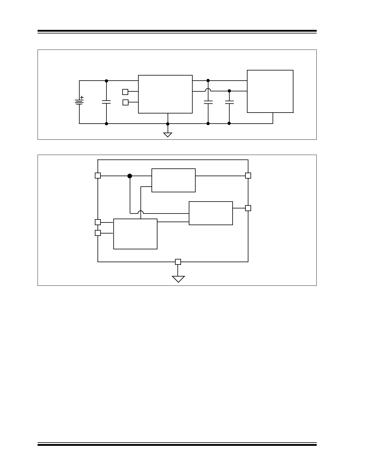
Typical Application Circuit
Functional Block Diagram
MIC5331
TDFN-8
MIC5331-xxYMT
I/O
CORE
Camera DSP
VIN
EN2
VOUT1
VOUT2
GND
EN1
1μF
VBAT
1μF
1μF
EN1
Reference
Enable
Thermal
Shutdown
LDO1
EN2
LDO2
VIN
VOUT1
VOUT2
GND
2017 Microchip Technology Inc.
DS20005874A-page 3
MIC5331
1.0
ELECTRICAL CHARACTERISTICS
Absolute Maximum Ratings †
Supply Voltage (V
IN
) ......................................................................................................................................... 0V to +6V
Enable Input Voltage (V
EN1
, V
EN2
) .....................................................................................................................0V to V
IN
Power Dissipation (P
D
,
Note 1
).............................................................................................................. Internally Limited
ESD Rating .............................................................................................................................................................
Note 2
Operating Ratings ‡
Supply Voltage (V
IN
) ................................................................................................................................. +2.3V to +5.5V
Enable Input Voltage (V
EN1
, V
EN2
) .....................................................................................................................0V to V
IN
†
Notice: Stresses above those listed under “Absolute Maximum Ratings” may cause permanent damage to the device.
This is a stress rating only and functional operation of the device at those or any other conditions above those indicated
in the operational sections of this specification is not intended. Exposure to maximum rating conditions for extended
periods may affect device reliability.
‡ Notice:
The device is not guaranteed to function outside its operating ratings.
Note 1:
The maximum allowable power dissipation of any T
A
(ambient temperature) is P
D(max)
= (T
J(max)
– T
A
)/θ
JA
.
Exceeding the maximum allowable power dissipation will result in excessive die temperature, and the reg-
ulator will go into thermal shutdown.
2:
Devices are ESD sensitive. Handling precautions recommended.
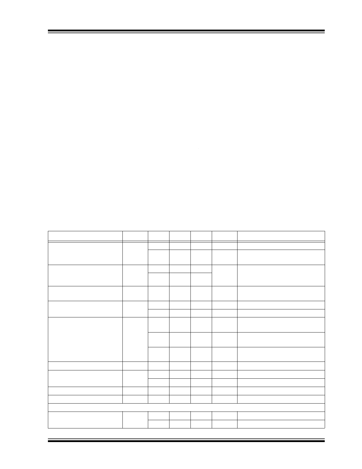
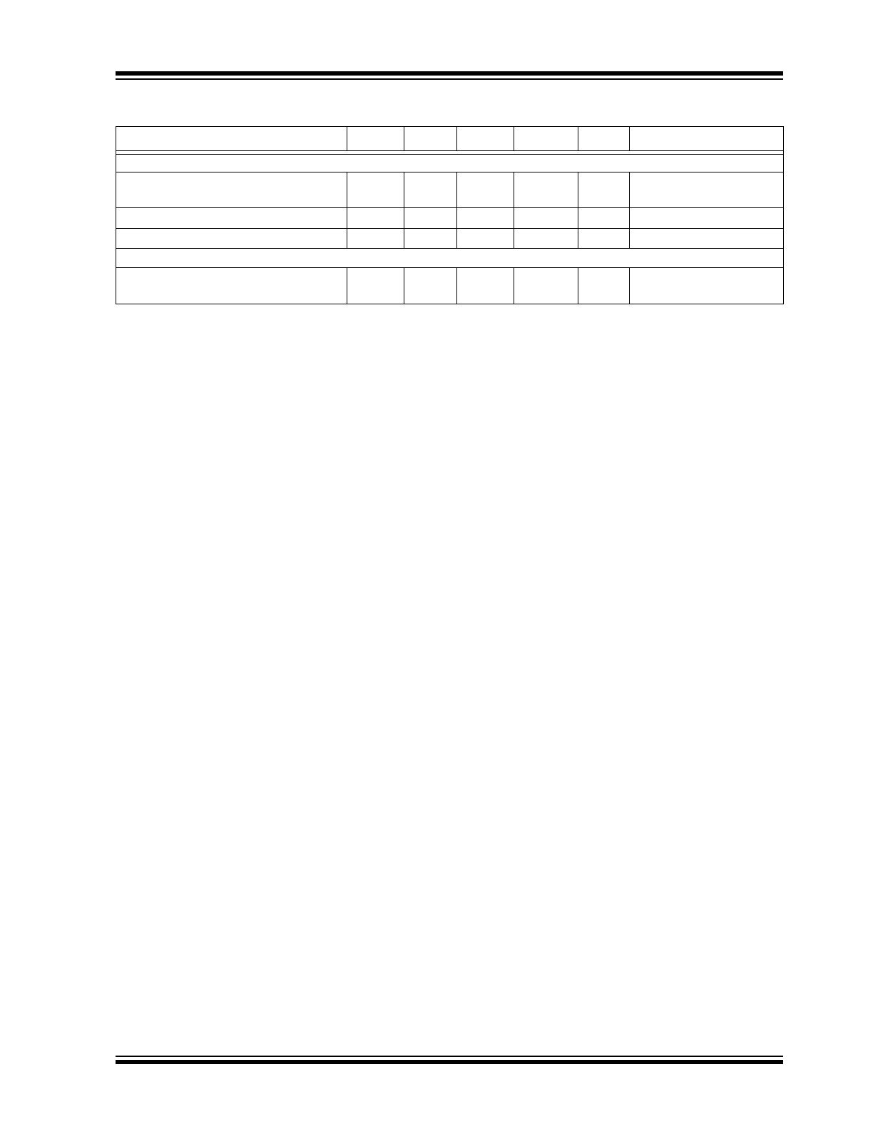
TABLE 1-1:
ELECTRICAL CHARACTERISTICS
Electrical Characteristics:
V
IN
= V
EN1
= V
EN2
= V
OUT
+ 1.0V, higher of the two regulator outputs; I
OUT1
= I
OUT2
=
100 µA; C
OUT1
= C
OUT2
= 1 µF; T
J
= +25°C, bold values indicate –40°C ≤ T
J
≤ +125°C; unless noted.
Note 1
Parameter
Symbol
Min.
Typ.
Max.
Units
Conditions
Output Voltage Accuracy
∆V
OUT
–1.0
—
1.0
%
Variation from nominal V
OUT
–2.0
—
2.0
%
Variation from nominal V
OUT
;
–40°C to +125°C
Line Regulation
∆V
OUT
/
(V
OUT
x
∆V
IN
)
—
0.02
0.3
%/V
V
IN
= V
OUT
+1V to 5.5V;
I
OUT
= 100 µA
—
—
0.6
Load Regulation
∆V
OUT
/
V
OUT
—
0.2
0.5
%
I
OUT
= 100 µA to 300 mA
Dropout Voltage
V
DO
—
20
40
mV
I
OUT
= 50 mA
—
120
240
mV
I
OUT
= 300 mA
Ground Current
I
GND
—
25
50
µA
V
EN1
= High; V
EN2
= Low;
I
OUT
= 100 µA to 300 mA
—
25
50
µA
V
EN1
= Low; V
EN2
= High;
I
OUT
= 100 µA to 300 mA
—
40
75
µA
V
EN1
= V
EN2
= High;
I
OUT1
= 300 mA, I
OUT2
= 300 mA
Ground Current in Shutdown
I
SHDN
—
0.01
1.0
µA
V
EN1
= V
EN2
< 0.2V
Ripple Rejection
PSRR
—
65
—
dB
f = 1 kHz; C
OUT
= 2.2 µF
—
45
—
dB
f = 20 kHz; C
OUT
= 2.2 µF
Current Limit
I
LIMIT
350
550
800
mA
V
OUT
= 0V
Output Voltage Noise
e
N
—
50
—
µV
RMS
C
OUT
= 1 µF; 10 Hz to 100 kHz
Enable Inputs (EN1/EN2)
Enable Input Voltage
V
ENABLE
—
—
0.2
V
Logic Low
1.2
—
—
V
Logic High
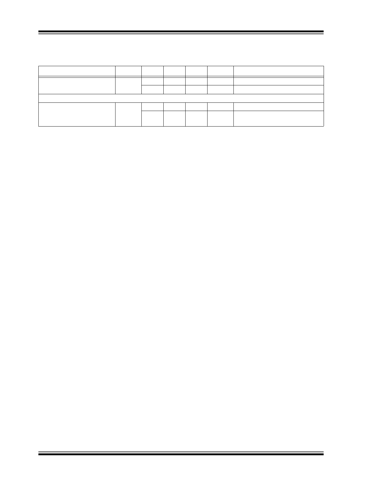
MIC5331
DS20005874A-page 4
2017 Microchip Technology Inc.
Enable Input Current
I
ENABLE
—
0.01
1.0
µA
V
IL
≤ 0.2V
—
0.01
1.0
µA
V
IH
≥ 1.2V
Turn-On Time
Turn-On Time (LDO1 and 2)
t
ON
—
140
500
µs
C
OUT
= 1 µF (Enable of First LDO)
—
110
500
µs
C
OUT
= 1 µF (Enable of Second
LDO after First Enabled)
Note 1:
Specification for packaged product only.
TABLE 1-1:
ELECTRICAL CHARACTERISTICS (CONTINUED)
Electrical Characteristics:
V
IN
= V
EN1
= V
EN2
= V
OUT
+ 1.0V, higher of the two regulator outputs; I
OUT1
= I
OUT2
=
100 µA; C
OUT1
= C
OUT2
= 1 µF; T
J
= +25°C, bold values indicate –40°C ≤ T
J
≤ +125°C; unless noted.
Note 1
Parameter
Symbol
Min.
Typ.
Max.
Units
Conditions
2017 Microchip Technology Inc.
DS20005874A-page 5
MIC5331
TEMPERATURE SPECIFICATIONS (
Note 1
)
Parameters
Sym.
Min.
Typ.
Max.
Units
Conditions
Temperature Ranges
Junction Operating Temperature
Range
T
J
–40
—
+125
°C
—
Storage Temperature Range
T
S
–65
—
+150
°C
—
Lead Temperature
—
—
—
+260
°C
Soldering, 3s
Package Thermal Resistances
Thermal Resistance 2 mm x 2 mm
TDFN 8-Ld
JA
—
90
—
°C/W
—
Note 1:
The maximum allowable power dissipation is a function of ambient temperature, the maximum allowable
junction temperature and the thermal resistance from junction to air (i.e., T
A
, T
J
,
JA
). Exceeding the
maximum allowable power dissipation will cause the device operating junction temperature to exceed the
maximum +125°C rating. Sustained junction temperatures above +125°C can impact the device reliability.
MIC5331
DS20005874A-page 6
2017 Microchip Technology Inc.
2.0
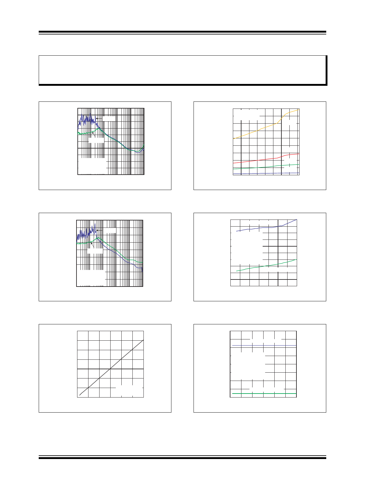
TYPICAL PERFORMANCE CURVES
FIGURE 2-1:
Power Supply Rejection
Ratio.
FIGURE 2-2:
Power Supply Rejection
Ratio.
FIGURE 2-3:
Dropout Voltage vs. Load
Current.
FIGURE 2-4:
Dropout Voltage vs.
Temperature.
FIGURE 2-5:
Ground Current vs. Supply
Voltage.
FIGURE 2-6:
Ground Current vs. Load
Current.
Note:
The graphs and tables provided following this note are a statistical summary based on a limited number of
samples and are provided for informational purposes only. The performance characteristics listed herein
are not tested or guaranteed. In some graphs or tables, the data presented may be outside the specified
operating range (e.g., outside specified power supply range) and therefore outside the warranted range.
0
-10
-20
-30
-40
-50
-60
-70
-80
-90
-100
dB
100
1K
10K
100K
1M
FREQUENCY (Hz)
50mA
300mA
V
IN
= 2.3V
V
OUT
= 1.2V
C
OUT
= 2.2μF
10
0
-10
-20
-30
-40
-50
-60
-70
-80
-90
dB
100
1K
10K
100K
1M
FREQUENCY (Hz)
50mA
300mA
V
IN
= 2.3V
V
OUT
= 1.2V
C
OUT
= 1μF
10
0
0.02
0.04
0.06
0.08
0.10
0.12
0.14
0
50
100 150 200 250 300
DROPOUT VOLTAGE (V)
LOAD CURRENT (mA)
V
OUT
= 2.8V
C
OUT
= 1μF
0
0.02
0.04
0.06
0.08
0.10
0.12
0.14
0.16
0.18
DROPOUT VOLTAGE (V)
TEMPERATURE (°C)
V
OUT
= 2.8V
C
OUT
= 1μF
-40 -20 0
20 40 60 80 100 120
100mA
10mA
50mA
300mA
20
22
24
26
28
30
32
34
36
38
40
2
2.5
3
3.5
4
4.5
5
5.5
SUPPLY VOLTAGE (V)
GROUND CURRENT (μA)
V
OUT1
= 2.5V
V
OUT2
= 1.2V
C
OUT1
= 1μF
C
OUT2
= 1μF
I
OUT1
= 300mA
I
OUT2
= 300mA
Dual LDO Enabled
Single LDO Enabled
25
27
29
31
33
35
37
39
41
0
50
100 150 200 250 300
LOAD CURRENT (mA)
GROUND CURRENT (μA)
V
IN
= V
OUT
+ 1V
V
OUT1
= 2.5V
V
OUT2
= 1.2V
C
OUT1
= 1μF
C
OUT2
= 1μF
Dual LDO Enabled
Single LDO Enabled
2017 Microchip Technology Inc.
DS20005874A-page 7
MIC5331
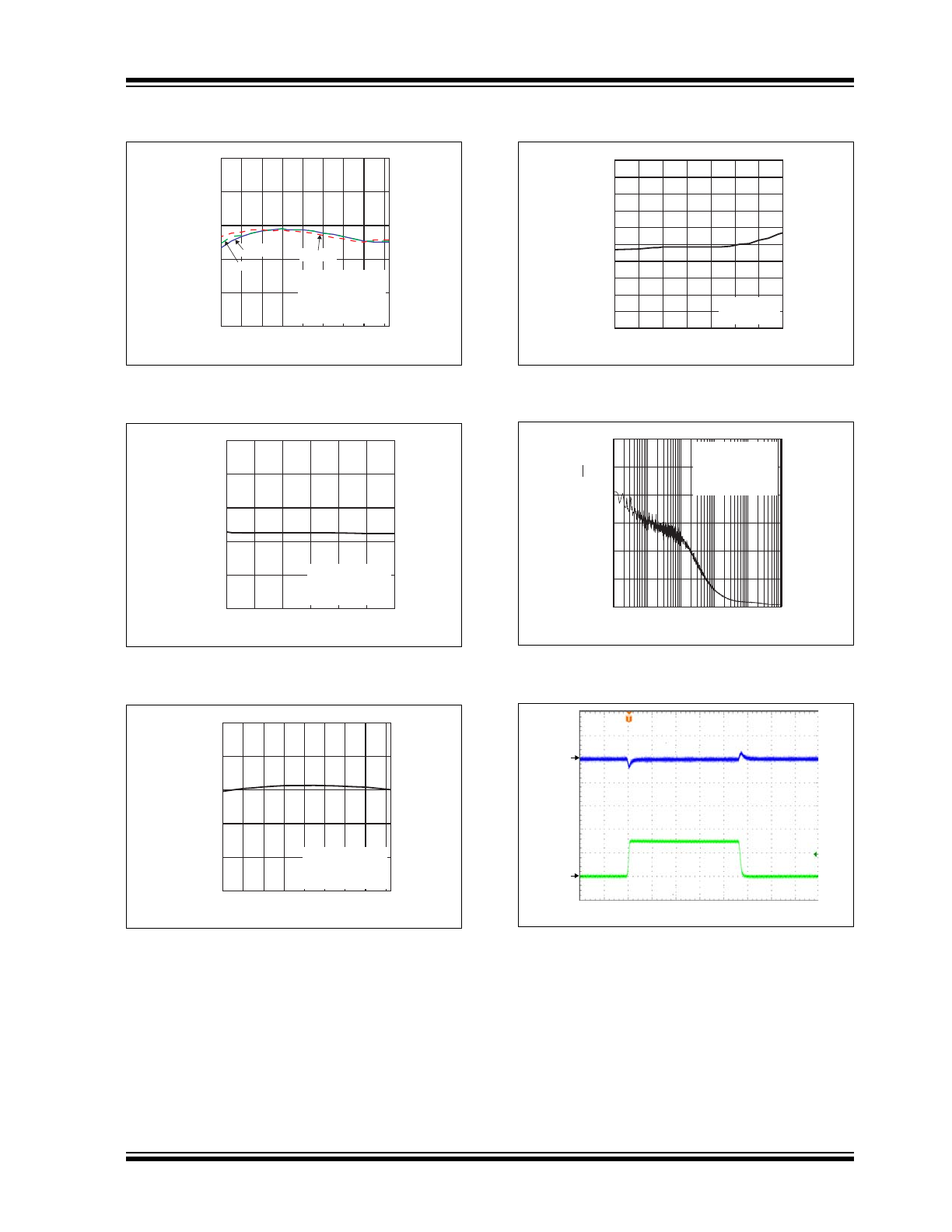
FIGURE 2-7:
Ground Current vs.
Temperature.
FIGURE 2-8:
Output Voltage vs. Load
Current.
FIGURE 2-9:
Output Voltage vs.
Temperature.
FIGURE 2-10:
Current Limit vs. Supply
Voltage.
FIGURE 2-11:
Output Noise Spectral
Density.
FIGURE 2-12:
Load Transient (0 mA –
150 mA).
30
33
36
39
42
45
GROUND CURRENT (μA)
EN1 = EN2 = V
IN
V
IN
= V
OUT
+ 1V
V
OUT
= 2.8V
C
OUT
= 1μF
100mA
300mA
10mA
TEMPERATURE (°C)
-40 -20 0
20 40 60 80 100 120
2.800
2.804
2.808
2.812
2.816
2.820
0
50
100 150 200 250 300
OUTPUT VOLTAGE (V)
LOAD CURRENT (mA)
V
IN
= V
OUT +
1V
V
OUT
= 2.8V
C
OUT
= 1μF
2.5
2.6
2.7
2.8
2.9
3.0
OUTPUT VOLTAGE (V)
V
IN
= V
OUT
+ 1V
V
OUT
= 2.8V
C
OUT
= 1μF
TEMPERATURE (°C)
-40 -20 0
20 40 60 80 100 120
350
400
450
500
550
600
650
700
750
800
850
2
2.5
3
3.5
4
4.5
5
5.5
CURRENT LIMIT (mA)
SUPPLY VOLTAGE (V)
C
IN
= 1μF
C
OUT
= 1μF
0
0.2
0.4
0.6
0.8
1.2
1.0
10
1K
10K 100K
FREQUENCY (Hz)
100
1M
V
IN
= V
OUT
+ 1V
V
OUT
= 2.8V
C
OUT
= 1μF
Load = 50mA
28738712,6(9¥+]
OUTPUT
CURRENT
(100mA/div)
LDO VOL
T
AGE
(50mV/div)
Time (100μs/div)
2.5V
0mA
150mA
MIC5331
DS20005874A-page 8
2017 Microchip Technology Inc.
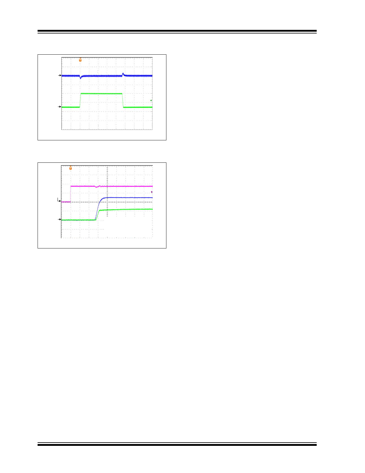
FIGURE 2-13:
Load Transient (150 mA –
300 mA)
.
FIGURE 2-14:
Enable Turn-On
.
OUTPUT
CURRENT
(100mA/div)
LDO VOL
T
AGE
(50mV/div)
Time (100μs/div)
2.5V
300mA
150mA
ENABLE
(2V/div)
LDO1/LDO2 VOL
T
AGE
(1V/div)
Time (40μs/div)
V
IN
= V
EN1
= V
EN2
= V
OUT1
+ 1V
V
OUT1
= 2.5V
V
OUT2
= 1.2V
C
IN
= 1μF
C
OUT1
= C
OUT2
= 1μF
LDO1
LDO2
2017 Microchip Technology Inc.
DS20005874A-page 9
MIC5331
3.0
PIN DESCRIPTIONS
The descriptions of the pins are listed in
Table 3-1
.
TABLE 3-1:
PIN FUNCTION TABLE
Pin Number
Pin Name
Description
1
VIN
Supply Input.
2
GND
Ground.
3
NC
Not Internally Connected.
4
EN2
Enable Input (Regulator 2): Active-High Input. Logic-High = On; Logic-Low = Off. Do
not leave floating.
5
EN1
Enable Input (Regulator 1): Active-High Input. Logic-High = On; Logic-Low = Off. Do
not leave floating.
6
NC
Not Internally Connected.
7
VOUT2
Regulator Output: LDO2.
8
VOUT1
Regulator Output: LDO1.
MIC5331
DS20005874A-page 10
2017 Microchip Technology Inc.
4.0
APPLICATION INFORMATION
MIC5331 is a tiny, dual, low quiescent current, 300 mA
LDO. The MIC5331 regulator is fully protected from
damage due to fault conditions, offering linear current
limiting and thermal shutdown.
4.1
Input Capacitor
The MIC5331 is a high-performance, high bandwidth
device. Therefore, it requires a well-bypassed input
supply for optimal performance. A 1 µF capacitor is
required from the input to ground to provide stability.
Low-ESR ceramic capacitors provide optimal
performance at a minimum of space. Additional
high-frequency capacitors, such as small-valued NPO
dielectric-type capacitors, help filter out high-frequency
noise and are good practice in any RF-based circuit.
X5R or X7R dielectrics are recommended for the input
capacitor. Y5V dielectrics lose most of their
capacitance over temperature and are therefore, not
recommended.
4.2
Output Capacitor
The MIC5331 requires an output capacitor of 1 µF or
greater to maintain stability. The design is optimized for
use with low-ESR ceramic chip capacitors. High ESR
capacitors may cause high frequency oscillation. The
output capacitor can be increased, but performance
has been optimized for a 1 µF ceramic output capacitor
and does not improve significantly with larger
capacitance.
X7R/X5R dielectric-type ceramic capacitors are
recommended because of their temperature
performance. X7R-type capacitors change capacitance
by 15% over their operating temperature range and are
the most stable type of ceramic capacitors. Z5U and
Y5V dielectric capacitors change value by as much as
50% and 60%, respectively, over their operating
temperature ranges. To use a ceramic chip capacitor
with Y5V dielectric, the value must be much higher than
an X7R ceramic capacitor to ensure the same
minimum capacitance over the equivalent operating
temperature range.
4.3
No-Load Stability
Unlike many other voltage regulators, the MIC5331 will
remain stable and in regulation with no load. This is
especially important in CMOS RAM keep-alive
applications.
4.4
Enable/Shutdown
The MIC5331 comes with dual active-high enable pins
that allow each regulator to be disabled independently.
Forcing the enable pin low disables the regulator and
sends it into a “zero” off-mode-current state. In this
state, current consumed by the regulator goes nearly to
zero. Forcing the enable pin high enables the output
voltage. The active-high enable pin uses CMOS
technology and the enable pin cannot be left floating; a
floating enable pin may cause an indeterminate state
on the output.
4.5
Thermal Considerations
The MIC5331 is designed to provide 300 mA of
continuous current for both outputs in a very small
package. Maximum ambient operating temperature
can be calculated based on the output current and the
voltage drop across the part. For example, if the input
voltage is 3.6V, the output voltage is 3.0V for V
OUT1
,
2.8V for V
OUT2
and the output current equals 300 mA
for each output. The actual power dissipation of the
regulator circuit can be determined using
Equation 4-1
:
EQUATION 4-1:
Because this device is CMOS and the ground current
is typically <100 µA over the load range, the power
dissipation contributed by the ground current is <1%
and can be ignored for this calculation.
EQUATION 4-2:
To determine the maximum ambient operating
temperature of the package, use the
junction-to-ambient thermal resistance of the device
and the following basic equation:
EQUATION 4-3:
P
D
V
IN
V
OUT1
–
I
OUT1
V
IN
V
OUT2
–
I
OUT2
V
IN
I
GND
+
+
=
P
D
3.6V
3.0V
–
300mA
3.6V
2.8V
–
300mA
+
0.42W
=
=
P
D MAX
T
J MAX
T
A
–
JA
--------------------------------
=
Where:
T
J(MAX)
= 125°C
θ
JA
= 90°C/W