
2016 Microchip Technology Inc.
DS20005677A-page 1
MIC5021
Features
• 12V to 36V Operation
• 550 ns Rise/Fall Time Driving 2000 pF
• TTL-Compatible Input with Internal Pull-Down
Resistor
• Overcurrent Limit
• Gate-to-Source Protection
• Internal Charge Pump
• 100 kHz Operation Guaranteed Over Full Tem-
perature and Operating Voltage Range
• Compatible with Current-Sensing MOSFETs
• Current-Source Drive Reduces EMI
Applications
• Lamp Control
• Heater Control
• Motor Control
• Solenoid Switching
• Switch-Mode Power Supplies
• Circuit Breaker
General Description
The MIC5021 high-side MOSFET driver is designed to
operate at frequencies up to 100 kHz (5 kHz PWM for
2% to 100% duty cycle) and is an ideal choice for high
speed applications such as motor control, SMPS
(switch mode power supplies), and applications using
IGBTs. The MIC5021 can also operate as a circuit
breaker with or without automatic retry.
A rising or falling edge on the input results in a current
source pulse or sink pulse on the gate output. This out-
put current pulse can turn on a 2000 pF MOSFET in
approximately 550 ns. The MIC5021 then supplies a
limited current (<2 mA), if necessary, to maintain the
output state.
An overcurrent comparator with a trip voltage of 50 mV
makes the MIC5021 ideal for use with a current-sens-
ing MOSFET. An external low value resistor may be
used instead of a sensing MOSFET for more precise
overcurrent control. An optional external capacitor
placed from the C
T
pin to ground may be used to con-
trol the current shutdown duty cycle (dead time) from
20% to <1%. A duty cycle from 20% to about 75% is
possible with an optional pull-up resistor from C
T
to
V
DD
. Additional parts of the MIC502x family include the
MIC5020 low-side driver and the MIC5022 half-bridge
driver with a cross-conduction interlock. The MIC5021
is available in 8-pin SOIC and plastic DIP packages.
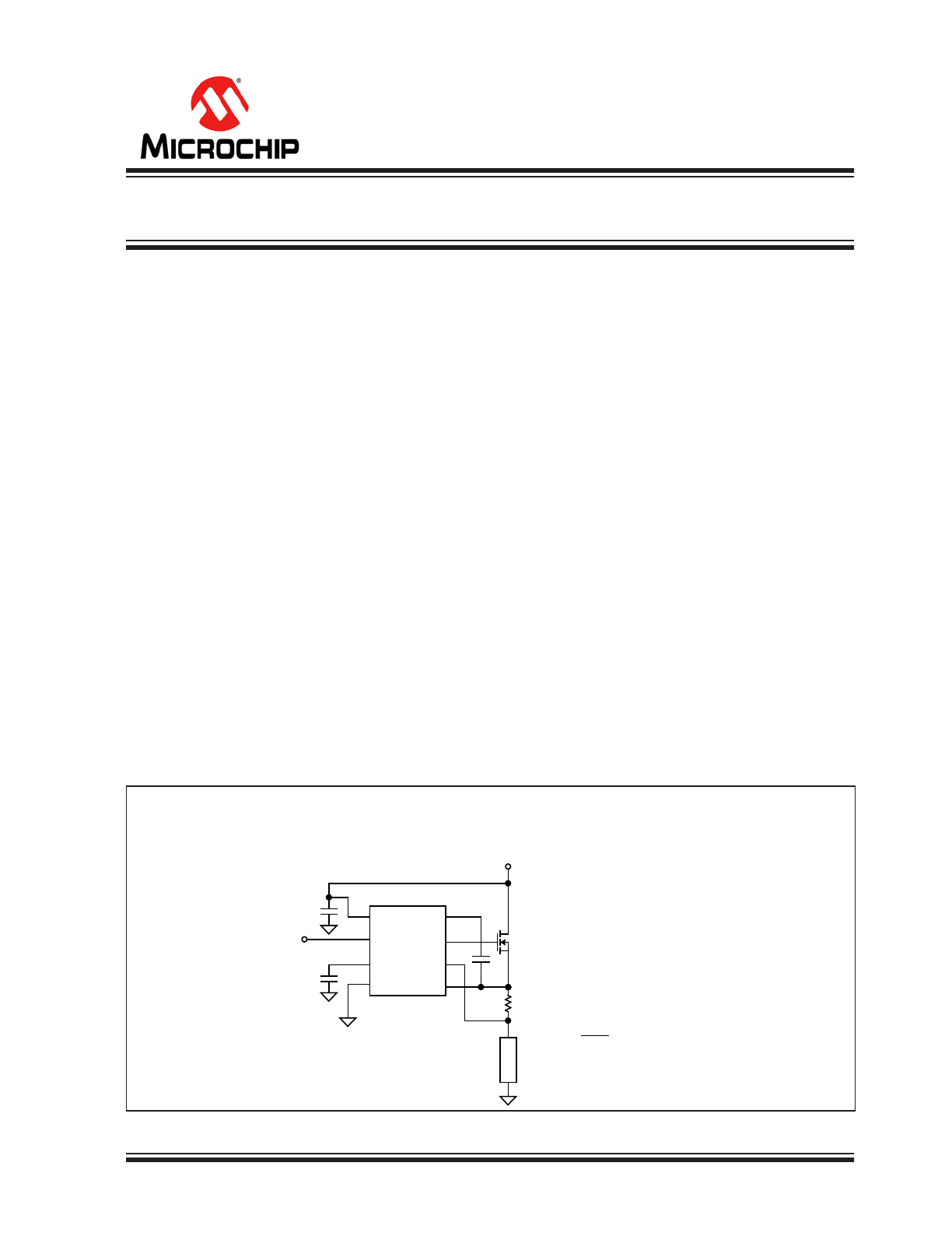
Typical Application Circuit
MIC5021
PDIP & SOIC
High-Side Driver with Overcurrent Trip and Retry
V
DD
INPUT
C
T
GND
V
B OOS T
GATE
SENSE-
SENSE+
TTL INPUT
R
S E N S E
N-CHANNEL
POWER MOSFET
+12V to +36V
MIC5021
1
2
3
4
8
7
6
5
10μF
2.7
nF
LOAD
R
S E N S E =
50mV
I
TR IP
* INCREASES TIME BEFORE RETRY
OPTIONAL*
High-Speed, High-Side MOSFET Driver with Charge Pump
and Overcurrent Limit
MIC5021
DS20005677A-page 2
2016 Microchip Technology Inc.
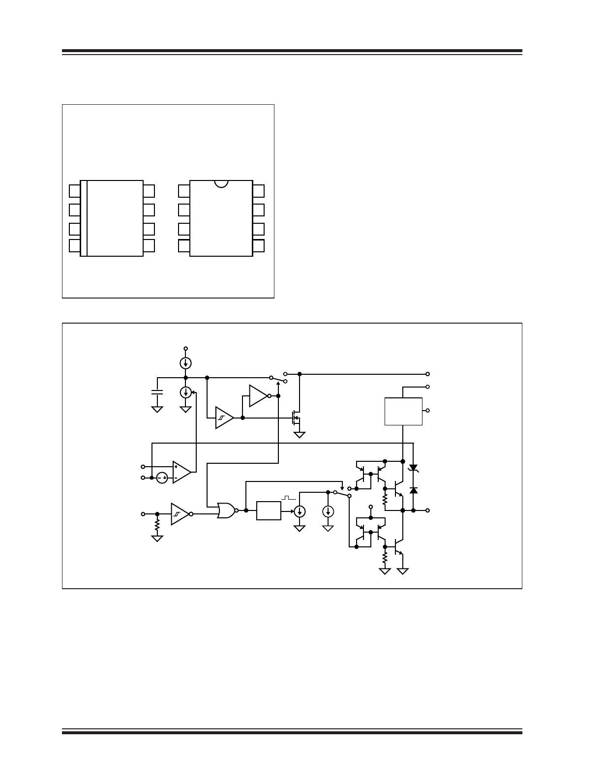
Package Types
Functional Block Diagram
MIC5021
SOIC
Top View
MIC5021
PDIP
Top View
1
2
3
4
8
7
6
5
V
B OOS T
GATE
SENSE-
SENSE+
V
DD
INPUT
C
T
GND
1
2
3
4
8
7
6
5
V
DD
INPUT
C
T
GND
V
B OOS T
GATE
SENSE-
SENSE+
SENSE-
SENSE+
6V INTERNAL REGULATOR
C
INT
I
1
2I
1
50mV
INPUT
ONE-
SHOT
GATE
C
T
6V
OFF
ON
FAULT
NORMAL
I
2
10I
2
15V
Q1
C H A R G E
PUMP
V
DD
V
B OOS T
↓
↑
TRANSISTOR: 106

2016 Microchip Technology Inc.
DS20005677A-page 3
MIC5021
1.0
ELECTRICAL CHARACTERISTICS
Absolute Maximum Ratings †
Supply Voltage, V
DD
................................................................................................................................................. +40V
Input Voltage, V
IN
....................................................................................................................................... –0.5V to +15V
Sense Differential Voltage........................................................................................................................................±6.5V
SENSE+ or SENSE– to GND .................................................................................................................... –0.5V to +36V
Timer Voltage .......................................................................................................................................................... +5.5V
V
BOOST
Capacitor ................................................................................................................................................ 0.01 μF
Operating Ratings
Supply Voltage, V
DD
.................................................................................................................................... +12V to +36V
†
Notice: Stresses above those listed under “Absolute Maximum Ratings” may cause permanent damage to the device.
This is a stress rating only and functional operation of the device at those or any other conditions above those indicated
in the operational sections of this specification is not intended. Exposure to maximum rating conditions for extended
periods may affect device reliability.
DC CHARACTERISTICS
Electrical Characteristics:
Unless otherwise indicated, T
A
= +25°C, GND = 0V, V
DD
= 12V, C
T
= OPEN,
Gate C
L
= 1500 pF (IRF540 MOSFET).
Parameters
Sym.
Min.
Typ.
Max.
Units
Conditions
DC Supply Current
—
—
1.8
4
mA
V
DD
= 12V, Input = 0V
—
—
2.5
6
V
DD
= 36V, Input = 0V
—
—
1.7
4
V
DD
= 12V, Input = 5V
—
—
2.5
6
V
DD
= 36V, Input = 5V
Input Threshold
—
0.8
1.4
2.0
V
—
Input Hysteresis
—
—
0.1
—
V
—
Input Pull-Down Current
—
10
20
40
μA
Input = 5V
Current-Limit Threshold
—
30
50
70
mV
Note 1
Gate On Voltage
—
16
18
21
V
V
DD
= 12V (
Note 2
)
—
46
50
52
V
DD
= 36V (
Note 2
)
Gate On-Time (Fixed)
t
G(ON)
2
6
10
μs
Sense Differential
70 mV
(
Note 8
)
Gate Off-Time (Adjustable)
t
G(OFF)
10
20
50
μs
Sense Differential
70 mV,
C
T
= 0 pF (
Note 8
)
Gate Turn-On Delay
t
DLH
—
500
1000
ns
Note 3
Gate Rise Time
t
R
—
400
500
ns
Note 4
Gate Turn-Off Delay
t
DLH
—
800
1500
ns
Note 5
Note 1:
When using sense MOSFETs, it is recommended that R
SENSE
< 50Ω. Higher values may affect the sense
MOSFET’s current transfer ratio.
2:
DC measurement.
3:
Input switched from 0.8V (TTL low) to 2.0V (TTL high), time for gate transition from 0V to 2V.
4:
Input switched from 0.8V (TTL low) to 2.0V (TTL high), time for gate transition from 2V to 17V.
5:
Input switched from 2.0V (TTL high) to 0.8V (TTL low), time for gate transition from 20V (gate on voltage)
to 17V.
6:
Input switched from 2.0V (TTL high) to 0.8V (TTL low), time for gate transition from 17V to 2V.
7:
Frequency where gate on voltage reduces to 17V with 50% input duty cycle.
8:
Gate on time t
G(ON)
and t
G(OFF)
are not 100% production tested.

MIC5021
DS20005677A-page 4
2016 Microchip Technology Inc.
Gate Fall Time
t
F
—
400
500
ns
Note 6
Max. Operating Frequency
f
MAX
100
150
—
kHz
Note 7
DC CHARACTERISTICS (CONTINUED)
Electrical Characteristics:
Unless otherwise indicated, T
A
= +25°C, GND = 0V, V
DD
= 12V, C
T
= OPEN,
Gate C
L
= 1500 pF (IRF540 MOSFET).
Parameters
Sym.
Min.
Typ.
Max.
Units
Conditions
Note 1:
When using sense MOSFETs, it is recommended that R
SENSE
< 50Ω. Higher values may affect the sense
MOSFET’s current transfer ratio.
2:
DC measurement.
3:
Input switched from 0.8V (TTL low) to 2.0V (TTL high), time for gate transition from 0V to 2V.
4:
Input switched from 0.8V (TTL low) to 2.0V (TTL high), time for gate transition from 2V to 17V.
5:
Input switched from 2.0V (TTL high) to 0.8V (TTL low), time for gate transition from 20V (gate on voltage)
to 17V.
6:
Input switched from 2.0V (TTL high) to 0.8V (TTL low), time for gate transition from 17V to 2V.
7:
Frequency where gate on voltage reduces to 17V with 50% input duty cycle.
8:
Gate on time t
G(ON)
and t
G(OFF)
are not 100% production tested.

2016 Microchip Technology Inc.
DS20005677A-page 5
MIC5021
TEMPERATURE SPECIFICATIONS (
Note 1
)
Parameters
Sym.
Min.
Typ.
Max.
Units
Conditions
Junction Thermal Resistances
Thermal Resistance, PDIP-8Ld
JA
–40
—
85
°C
Maximum Ambient Tem-
perature
Thermal Resistance, SOIC-8Ld
JA
–40
—
85
°C
Maximum Ambient Tem-
perature
Note 1:
The maximum allowable power dissipation is a function of ambient temperature, the maximum allowable
junction temperature and the thermal resistance from junction to air (i.e., T
A
, T
J
,
JA
). Exceeding the
maximum allowable power dissipation will cause the device operating junction temperature to exceed the
maximum rating. Sustained junction temperatures above the maximum rating can impact the device
reliability.
MIC5021
DS20005677A-page 6
2016 Microchip Technology Inc.
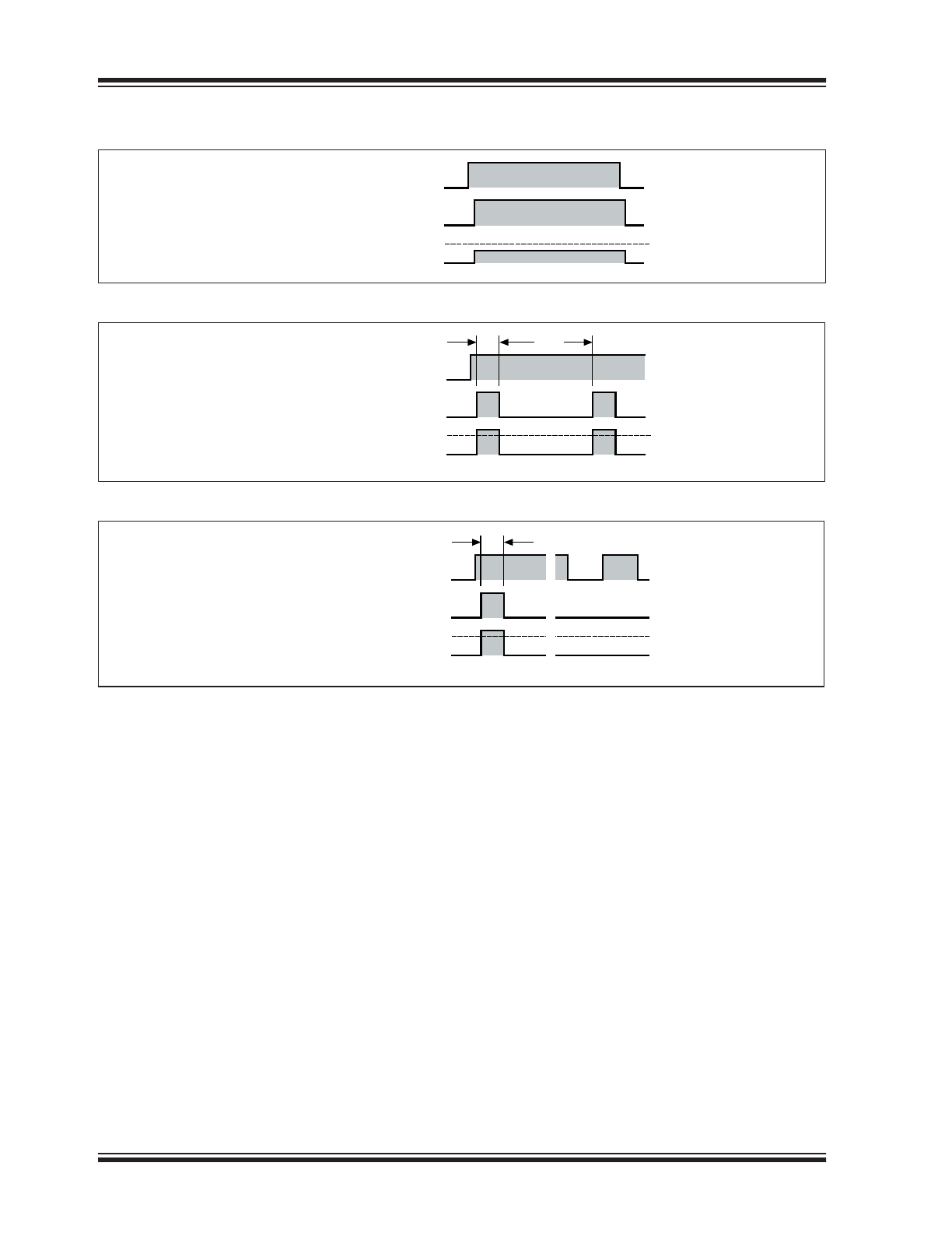
2.0
TIMING DIAGRAMS
FIGURE 2-1:
Normal operation.
FIGURE 2-2:
Fault Operation, C
T
= Open.
FIGURE 2-3:
Fault Condition, C
T
= Grounded.
INPUT
0V
TTL (H)
SOURCE
50mV
SENSE +,–
DIFFERENTIAL
GATE
0V
15V (MAX.)
INPUT
0V
TTL (H)
SOURCE
50mV
SENSE +,–
DIFFERENTIAL
GATE
0V
15V (MAX.)
6μs
20μs
INPUT
0V
TTL (H)
SOURCE
50mV
SENSE +,–
DIFFERENTIAL
GATE
0V
15V (MAX.)
6μs
2016 Microchip Technology Inc.
DS20005677A-page 7
MIC5021
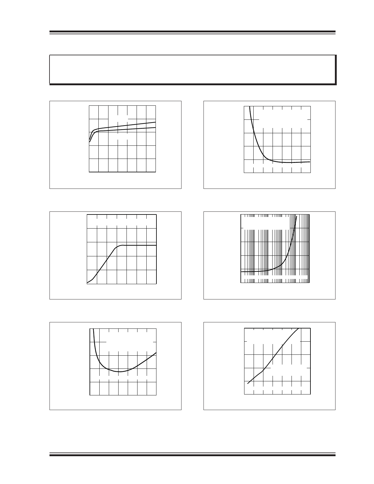
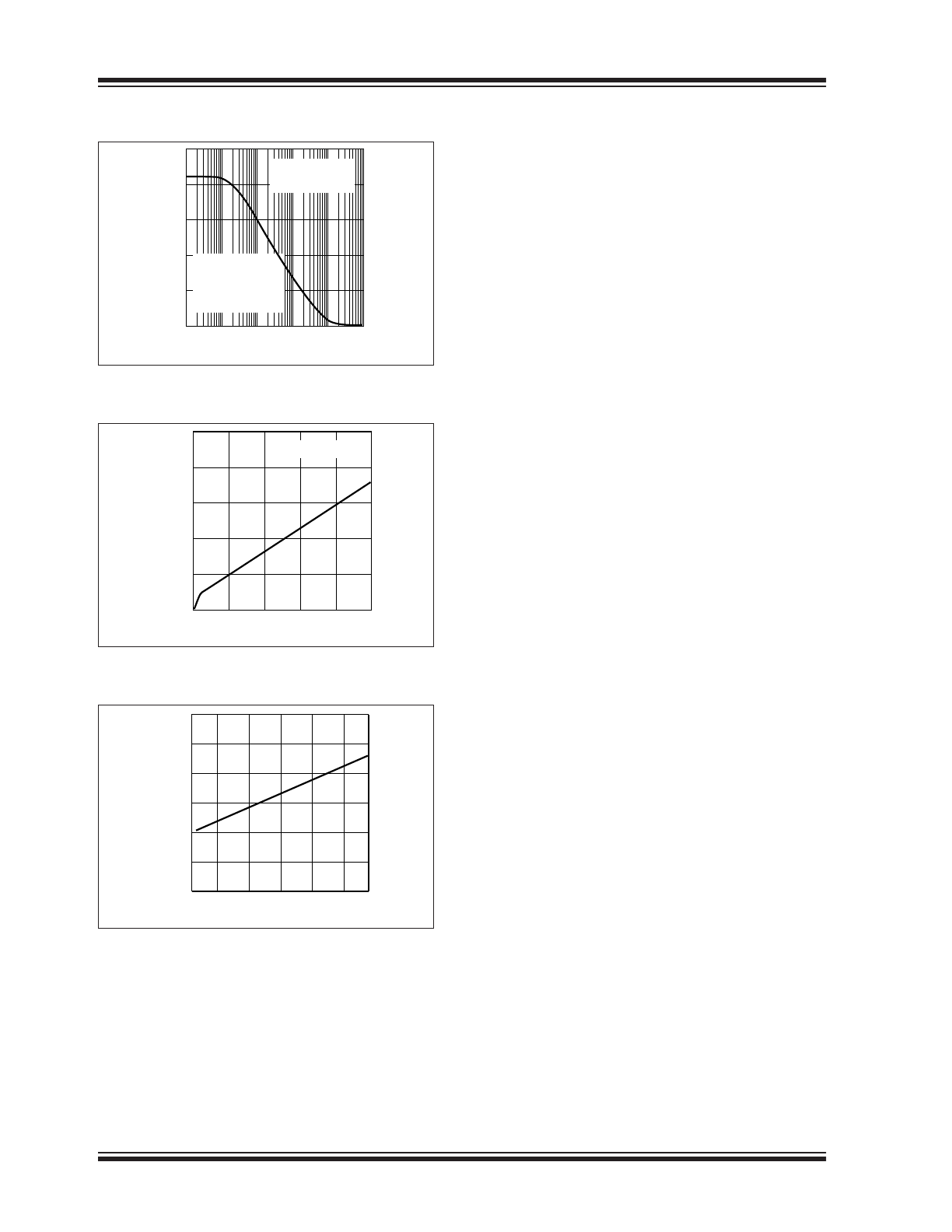
3.0
TYPICAL PERFORMANCE CURVES
FIGURE 3-1:
Supply Current vs. Supply
Voltage.
FIGURE 3-2:
Gate Voltage Change vs.
Supply Voltage.
FIGURE 3-3:
Gate Turn-On Delay vs.
Supply Voltage.
FIGURE 3-4:
Gate Turn-On Delay vs.
Supply Voltage.
FIGURE 3-5:
Gate Turn-On Delay vs.
Gate Capacitance.
FIGURE 3-6:
Gate Turn-Off Delay vs.
Supply Voltage.
Note:
The graphs and tables provided following this note are a statistical summary based on a limited number of
samples and are provided for informational purposes only. The performance characteristics listed herein
are not tested or guaranteed. In some graphs or tables, the data presented may be outside the specified
operating range (e.g., outside specified power supply range) and therefore outside the warranted range.
0.0
0.5
1.0
1.5
2.0
2.5
5
10
15
20
25
30
35
40
I
SUPPLY
(mA)
V
SUPPLY
(V)
V
IN
= 0V
V
IN
= 5V
0
5
10
15
20
25
5
10
15
20
25
30
35
40
V
GATE
(V)
V
SUPPLY
(V)
V
G AT E
= V
G AT E
– V
S U P P L Y
650
700
750
800
850
900
5
10
15
20
25
30
35
40
t
ON 4V
(ns)
V
SUPPLY
(V)
V
GATE
= V
SUPPLY
+ 4V
C
L
= 1500pF (IRCZ34)
C
BOOST
= 0.01μF
INCLUDES PROPAGATION DELAY
750
800
850
900
950
1000
5
10
15
20
25
30
35
40
t
ON 10V
(ns)
V
SUPPLY
(V)
V
GATE
= V
SUPPLY
+ 10V
C
L
= 1500pF (IRCZ34)
C
BOOST
= 0.01μF
INCLUDES PROPAGATION DELAY
0.0
0.5
1.0
1.5
2.0
2.5
1x10
0
1x10
1
1x10
2
1x10
3
1x10
4
1x10
5
t
ON
(μs)
C
GATE
(pF)
V
GATE
= V
SUPPLY
+ 4V
V
SUPPLY
= 12V
INCLUDES PROPAGATION DELAY
750
1000
1250
1500
1750
2000
5
10
15
20
25
30
35
40
t
OFF 4V
(ns)
V
SUPPLY
(V)
V
G AT E
= V
SUPPLY
+ 4V
R
L
= 400
INCLUDES PROPAGATION DELAY
C
G AT E
= 1500pF
(IRCZ34)
MIC5021
DS20005677A-page 8
2016 Microchip Technology Inc.
FIGURE 3-7:
Overcurrent Retry Duty
Cycle vs. Timing Capacitance.
FIGURE 3-8:
Input Current vs. Input
Voltage.
FIGURE 3-9:
Sense Threshold vs.
Temperature.
0
5
10
15
20
25
0.1
1
10
100 1000 10000
RETRY DUTY CYCLE (%)
C
T
(pF)
NOT E:
t
ON
, t
OFF
T I M E
INDEPENDENT
OF V
SUPPLY
t
ON
= 5μs
V
SUPPLY
= 12V
0
20
40
60
80
100
0
5
10
15
20
25
I
IN
(μ
A)
V
IN
(V)
V
SUPPLY
= 12V
20
30
40
50
60
80
0
20
40
60
80 100 120
VOLTAGE (mV)
TEMPERATURE (°C)
70

2016 Microchip Technology Inc.
DS20005677A-page 9
MIC5021
4.0
PIN DESCRIPTIONS
The descriptions of the pins are listed in
Table 4-1
.
TABLE 4-1:
PIN FUNCTION TABLE
Pin Number
Pin Name
Description
1
V
DD
Supply (+12V to 36V). Decouple with ≥ 10 μF capacitor.
2
INPUT
TTL-Compatible Input. Logic high turns the external MOSFET on. An internal
pull-down returns an open pin logic low.
3
CT
Retry Timing Capacitor. Controls the off time (t
G(OFF)
) of the overcurrent retry cycle
(duty cycle adjustment):
Open = Approximately 20% duty cycle.
Capacitor-to-Ground = Approximately 20% to <1% duty cycle.
Pull-Up Resistor = Approximately 20% to approximately 75% duty cycle.
Ground = Maintained shutdown upon overcurrent condition.
4
GND
Circuit Ground.
5
SENSE+
Current-Sense Comparator (+) Input. Connect to high side of sense resistor or cur-
rent sensing MOSFET sense lead. A built-in offset in conjunction with RSENSE
sets the load overcurrent trip point.
6
SENSE–
Current-Sense Comparator (–) Input. Connect to the low side of the sense resistor
(usually the high side of the load).
7
GATE
Gate Drive. Drives the gate of an external power MOSFET. Also limits V
GS
to 15V
maximum to prevent gate-to-source damage. Will sink-and-source current.
8
V
BOOST
Charge Pump Boost Capacitor. A bootstrap capacitor from V
BOOST
to the FET
source pin supplies charge to quickly enhance the gate output during turn-on.

MIC5021
DS20005677A-page 10
2016 Microchip Technology Inc.
5.0
FUNCTIONAL DESCRIPTION
Refer to the MIC5021
Functional Block Diagram
.
5.1
Input
A signal greater than 1.4V (nominal) applied to the
MIC5021 INPUT causes gate enhancement on an
external MOSFET turning the MOSFET on.
An internal pull-down resistor ensures that an open
input remains low, keeping the external MOSFET
turned off.
5.2
Gate Output
Rapid rise and fall times on the gate output are possible
because each input state change triggers a one-shot
which activates a high-value current sink (10I
2
) for a
short time. This draws a high current though a current
mirror circuit causing the output transistors to quickly
charge or discharge the external MOSFET’s gate.
A second current sink continuously draws the lower
value of current used to maintain the gate voltage for
the selected state.
An internal charge pump utilizes an external “boost”
capacitor connected between V
BOOST
and the source
of the external MOSFET (Refer to the
Typical Applica-
tion Circuit
). The boost capacitor stores charge when
the MOSFET is off. As the MOSFET turns on, its
source to ground voltage increases and is added to the
voltage across the capacitor, raising the V
BOOST
pin
voltage. The boost capacitor charge is directed through
the gate pin to quickly charge the MOSFET’s gate to
16V maximum above V
DD
. The internal charge pump
maintains the gate voltage.
An internal Zener diode protects the external MOSFET
by limiting the gate to source voltage.
5.3
SENSE Inputs
The MIC5021’s 50 mV (nominal) trip voltage is created
by internal current sources that force approximately
5 μA out of SENSE+ and approximately 15 μA (at trip)
out of SENSE–. When SENSE– is 50mV or more below
SENSE+, SENSE– steals base current from an internal
drive transistor shutting off the external MOSFET.
5.4
Overcurrent Limiting
Current source I1 charges C
INT
upon power up. An
optional external capacitor connected to C
T
is kept dis-
charged through a MOSFET Q1.
A fault condition (>50 mV from SENSE+ to SENSE–)
causes the overcurrent comparator to enable current
sink 2I
1
which overcomes current source I1 to dis-
charge C
INT
in a short time. When C
INT
is discharged,
the input is disabled, which turns off the gate output,
and C
INT
and C
T
are ready to be charged.
When the gate output turns the MOSFET off, the over-
current signal is removed from the sense inputs which
deactivates current sink 2I
1
.This allows C
INT
and the
optional capacitor connected to C
T
to recharge. A
Schmitt trigger delays the retry while the capacitor(s)
recharge. Retry delay is increased by connecting a
capacitor to C
T
(optional).
The retry cycle will continue until the fault is removed or
the input is changed to TTL low.
If C
T
is connected to ground, the circuit will not retry
upon a fault condition.