
2016 Microchip Technology Inc.
DS20005669A-page 1
MIC4930
Features
• Input Voltage: 2.7V to 5.5V
• 3A Output Current
• Up To 95% Efficiency
• Up To 3.3 MHz Operation
• Safe Start-Up into a Pre-Biased Output
• Power Good Output
• Ultra-Fast Transient Response
• Low Output Voltage Ripple
• Low R
DS(ON)
Integrated MOSFET Switches
• 0.01 μA Shutdown Current
• Thermal Shutdown and Current Limit Protection
• Output Voltage as low as 0.7V
• 3 mm × 4 mm DFN-10L
• –40°C to +125°C Junction Temperature Range
Applications
• DTVs
• Set-Top Boxes
• Printers
• DVD Players
• Distributed Power Supplies
General Description
The MIC4930 is a high-efficiency, 3A synchronous
buck regulator with ultra-fast transient response
perfectly suited for supplying processor core and I/O
voltages from a 5V or 3.3V bus. The MIC4930 provides
a switching frequency up to 3.3 MHz while achieving
peak efficiencies up to 95%. An additional benefit of
high-frequency operation is very low output ripple
voltage throughout the entire load range with the use of
a small output capacitor. The MIC4930 is designed for
use with a very small inductor, down to 1 μH, and an
output ceramic capacitor as small as 10 μF without the
need for external ripple injection. A wide range of
output capacitor types and values can also be
accommodated.
The MIC4930 supports safe start-up into a pre-biased
output.
The MIC4930 is available in a 10-pin 3 mm × 4 mm
DFN package with an operating junction temperature
range from –40°C to +125°C. The MIC4930 is
pin-to-pin compatible with the 5A-rated MIC4950YFL.
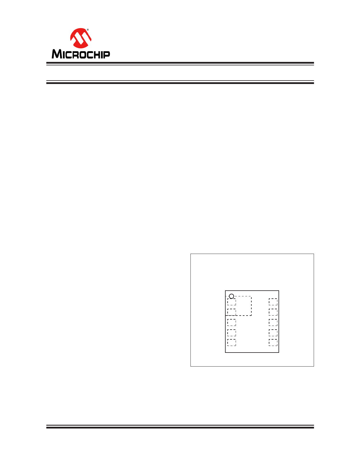
Package Type
MIC4930
3x4 DFN
Top View
AGND
FB
5
1
PGND
PGND
PVIN
AVIN
10 SW
EN
PVIN
PG
9
8
7
2
3
4
6
EP
Hyper Speed Control
®
3A Buck Regulator
MIC4930
DS20005669A-page 2
2016 Microchip Technology Inc.
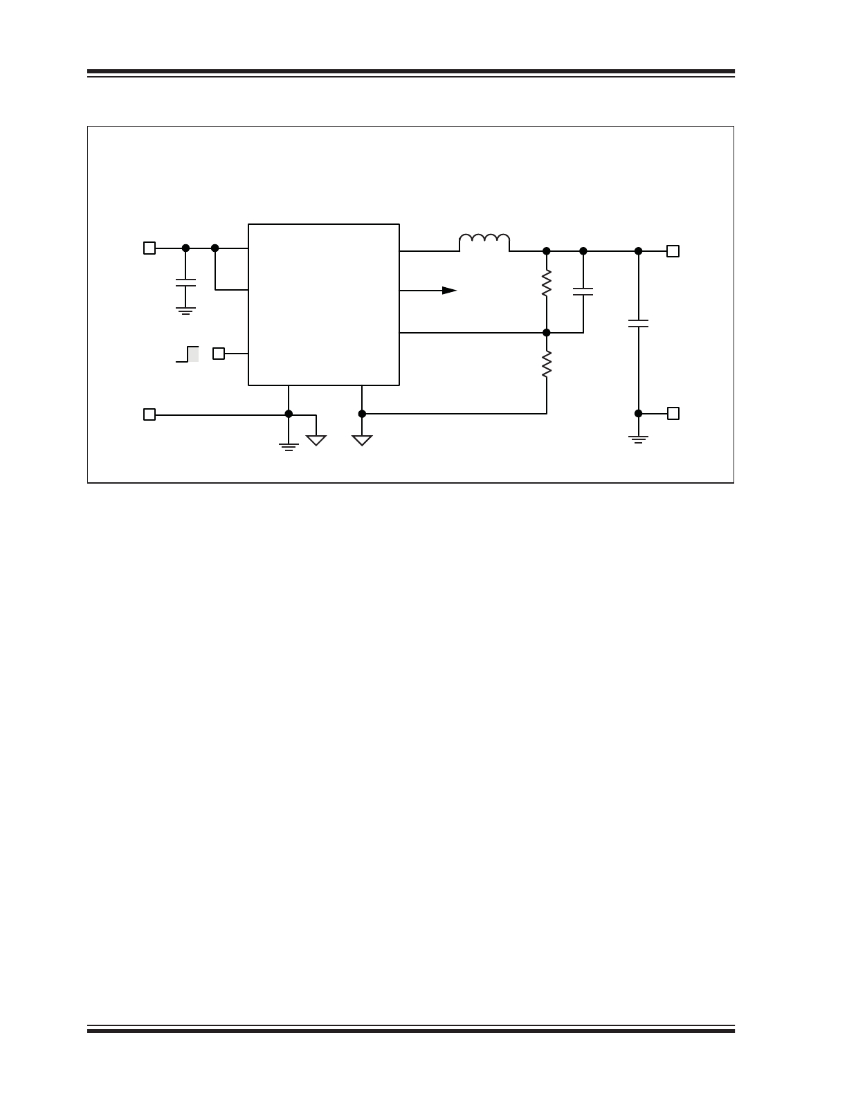
Typical Application Circuit
MIC4930
3x4 DFN-10L
MIC4930YFL
PVIN
EN
PGND
AGND
PG
SW
VIN
GND
GND
VOUT
OFF
ON
AVIN
FB
1μH
C
F
22pF
R1
301kΩ
R2
160kΩ
2.7V to 5.5V
10μF
10V
1.8V
C
OUT
10μF
2016 Microchip Technology Inc.
DS20005669A-page 3
MIC4930
1.0
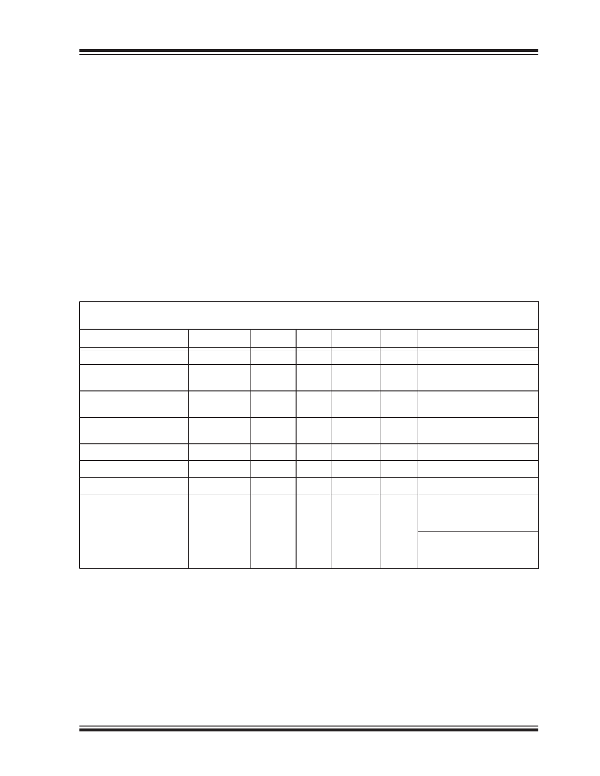
ELECTRICAL CHARACTERISTICS
Absolute Maximum Ratings †
PV
IN
, AV
IN
Supply Voltage (V
IN
)................................................................................................................... –0.3V to +6V
SW Output Switch Voltage (V
SW
).................................................................................................................. –0.3V to V
IN
EN, PG (V
EN
, V
PG
)........................................................................................................................................ –0.3V to V
IN
FB Feedback Input Voltage (V
FB
) ................................................................................................................ –0.3V to V
IN
ESD Protection On All Pins (
Note 1
) ...............................................................................................................±2 kV HBM
Operating Ratings ††
Supply Voltage (V
IN
) ................................................................................................................................. +2.7V to +5.5V
Enable Input Voltage (V
EN
) ............................................................................................................................... 0V to V
IN
†
Notice: Exceeding the absolute maximum ratings may damage the device.
††
Notice: The device is not guaranteed to function outside its operating ratings.
Note 1:
Devices are ESD sensitive. Handling precautions are recommended. Human body model, 1.5 kΩ in series
with 100 pF.
ELECTRICAL CHARACTERISTICS (
Note 1
)
Electrical Characteristics:
Unless otherwise indicated, V
IN
= V
EN
= 3.3V; L = 1.0 μH; T
A
= 25°C, C
IN
= 10 μH,
C
OUT
= 10 μH.
Parameters
Sym.
Min.
Typ.
Max.
Units
Conditions
Supply Voltage Range
V
IN
2.7
—
5.5
V
—
Undervoltage lockout
threshold
V
UVLO
2.41
2.5
2.61
V
(turn-on)
Undervoltage lockout
hysteresis
V
UVLOH
—
400
—
mV
—
Quiescent current
I
Q
—
0.8
2
mA
I
OUT
= 0 mA, FB >1.2 ×
V
FB(Nominal)
Shutdown current
I
SD
—
0.01
2
μA
V
EN
= 0V
Feedback voltage
V
FB
0.609
0.625
0.640
V
—
Current limit
I
LIMIT
3.5
5.75
8
A
FB = 0.9V × V
FB(Nominal)
Output voltage line
regulation
LINEREG
—
1
—
%/V
V
IN
= 2.7V to 3.5V, V
OUTNOM
= 1.8V,
I
LOAD
= 20 mA
V
IN
= 4.5V to 5.5V if
V
OUTNOM
≥2.5V,
I
LOAD
= 20 mA
Note 1:
Specification for packaged product only.
MIC4930
DS20005669A-page 4
2016 Microchip Technology Inc.
Output voltage load
regulation
LOADREG
—
0.3
—
%
20 mA < I
LOAD
< 500 mA,
V
IN
= 3.6V if V
OUTNOM
< 2.5V
20 mA < I
LOAD
< 500 mA,
V
IN
= 5.0V if
V
OUTNOM
≥ 2.5V
—
1
—
%
20 mA < I
LOAD
< 3A,
V
IN
= 3.6V
if V
OUTNOM
< 2.5V
20 mA < I
LOAD
< 3 mA,
V
IN
= 5.0V
if V
OUTNOM
≥ 2.5V
PWM switch ON
resistance
R
DSON-P
—
30
—
mΩ
I
SW
= 1A P-Channel
MOSFET
R
DSON-N
—
25
—
I
SW
= 1A N-Channel
MOSFET
Maximum turn-on time
t
ON
—
665
—
ns
V
IN
= 4.5V, V
FB
= 0.5V
—
1000
—
V
IN
= 3.0V, V
FB
= 0.5V
—
1120
—
V
IN
= 2.7V, V
FB
= 0.5V
Minimum turn-off time
t
OFF
—
176
—
ns
V
IN
= 3.0V, V
FB
= 0.5V
Soft-start time
t
SOFT-ON
—
500
—
μs
V
OUT
= 90% of V
OUTNOM
Enable threshold
V
EN
0.5
0.8
1.2
V
Turn-on
Enable input current
I
EN
0.1
1
μA
—
Power Good threshold
V
OUTPG
82
88
94
%
Rising
Power Good hysteresis
V
OUTPGH
—
7
—
%
—
Overtemperature
shutdown
T
SD
150
°C
—
Overtemperature
shutdown hysteresis
T
SDH
20
°C
—
ELECTRICAL CHARACTERISTICS (CONTINUED)(
Note 1
)
Electrical Characteristics:
Unless otherwise indicated, V
IN
= V
EN
= 3.3V; L = 1.0 μH; T
A
= 25°C, C
IN
= 10 μH,
C
OUT
= 10 μH.
Parameters
Sym.
Min.
Typ.
Max.
Units
Conditions
Note 1:
Specification for packaged product only.
2016 Microchip Technology Inc.
DS20005669A-page 5
MIC4930
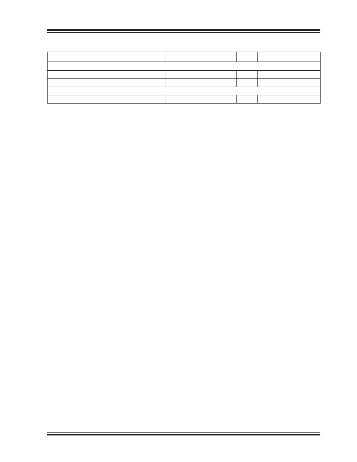
TEMPERATURE SPECIFICATIONS (
Note 1
)
Parameters
Sym.
Min.
Typ.
Max.
Units
Conditions
Temperature Ranges
Storage Temperature
T
S
–65
—
+150
°C
—
Junction Operating Temperature
T
J
–40
—
+125
°C
—
Package Thermal Resistances
Thermal Resistance, DFN-10Ld
JA
—
35
—
°C/W
—
Note 1:
The maximum allowable power dissipation is a function of ambient temperature, the maximum allowable
junction temperature and the thermal resistance from junction to air (i.e., T
A
, T
J
,
JA
). Exceeding the
maximum allowable power dissipation will cause the device operating junction temperature to exceed the
maximum +125°C rating. Sustained junction temperatures above +125°C can impact the device reliability.
MIC4930
DS20005669A-page 6
2016 Microchip Technology Inc.
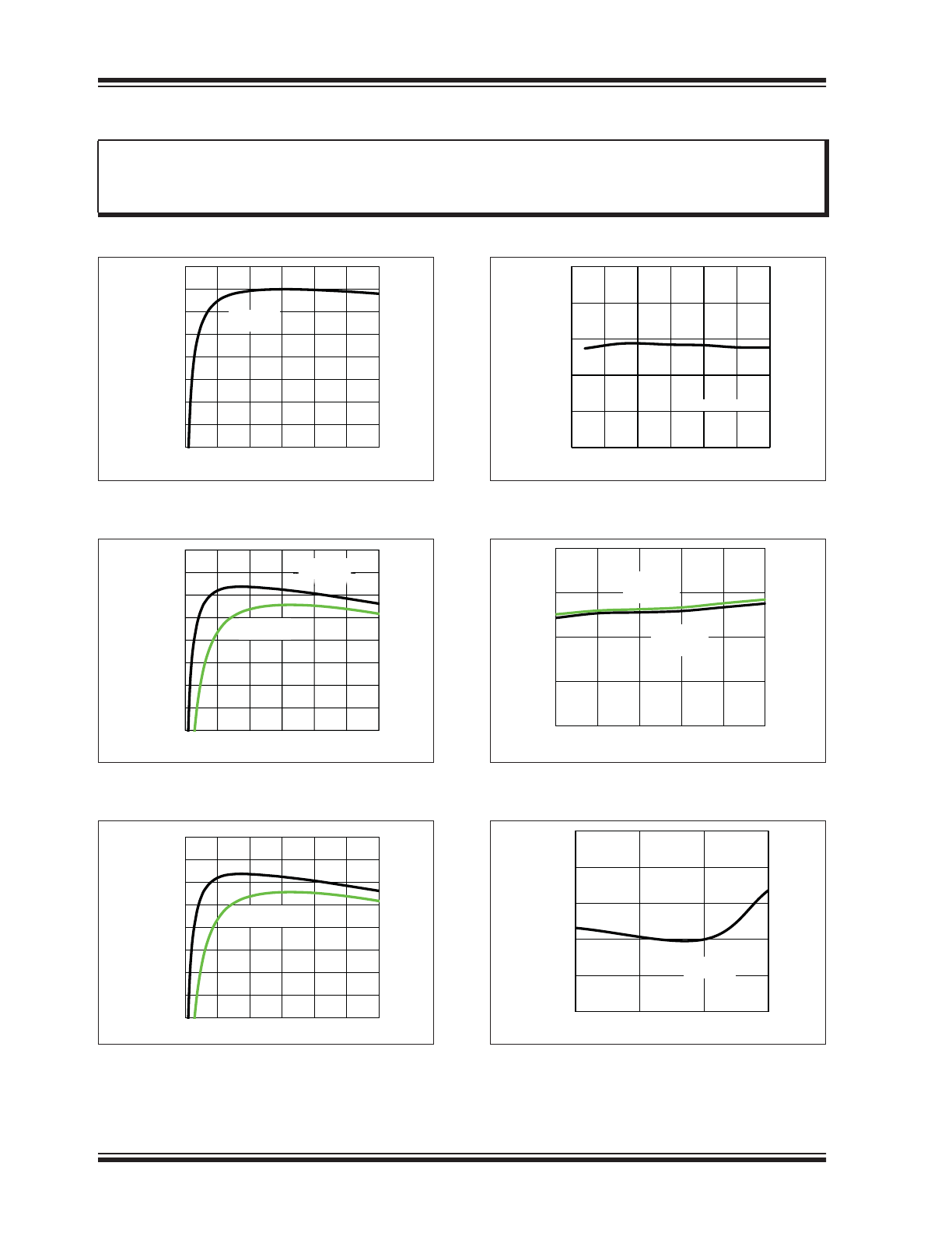
2.0
TYPICAL PERFORMANCE CURVES
FIGURE 2-1:
Efficiency vs. Output
Current.
FIGURE 2-2:
Efficiency vs. Output
Current.
FIGURE 2-3:
Efficiency vs. Output
Current.
FIGURE 2-4:
Current Limit vs. Input
Voltage.
FIGURE 2-5:
Current Limit vs. Feedback
Voltage.
FIGURE 2-6:
Line Regulation vs. Input
Voltage.
Note:
The graphs and tables provided following this note are a statistical summary based on a limited number of
samples and are provided for informational purposes only. The performance characteristics listed herein
are not tested or guaranteed. In some graphs or tables, the data presented may be outside the specified
operating range (e.g., outside specified power supply range) and therefore outside the warranted range.
60
65
70
75
80
85
90
95
100
0.0
0.5
1.0
1.5
2.0
2.5
3.0
EFFICIENCY
(%
)
OUTPUT CURRENT (A)
V
IN
= 5V
V
OUT
= 3.3V
60
65
70
75
80
85
90
95
100
0.0
0.5
1.0
1.5
2.0
2.5
3.0
EFFICIENCY
(%
)
OUTPUT CURRENT (A)
V
IN
= 5.0V
V
OUT
= 1.8V
V
IN
= 3.3V
V
OUT
= 1.8V
60
65
70
75
80
85
90
95
100
0.0
0.5
1.0
1.5
2.0
2.5
3.0
EFFICIENCY
(%
)
V
IN
= 5.0V
V
OUT
= 1.8V
V = 3.3V
V
OUT
= 1.8V
0
2
4
6
8
10
2.5
3.0
3.5
4.0
4.5
5.0
5.5
CURRENT LIMIT
(A
)
INPUT VOLTAGE (V)
V
OUT
= 1.8V
0
2
4
6
8
0.0
0.1
0.2
0.3
0.4
0.5
CURRENT LIMIT
(A
)
FEEDBACK VOLTAGE (V)
V
IN
= 5V
V
OUT
= 1.8V
V
IN
= 3.3V
V
OUT
= 1.8V
-2.0
-1.0
0.0
1.0
2.0
3.0
2.7
3.0
3.3
3.6
LINE REGULA
TION
(%
/V)
INPUT VOLTAGE (V)
V
OUT
= 1.8V
I
OUT
= 0A
V
OUT
= 1.8V
I
OUT
= 0A
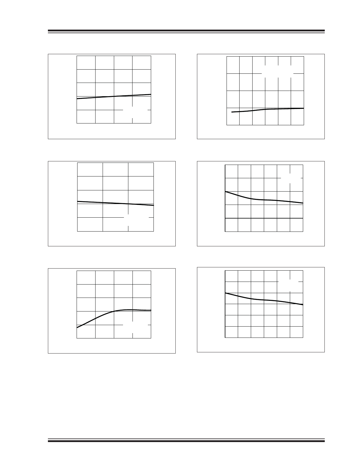
2016 Microchip Technology Inc.
DS20005669A-page 7
MIC4930
FIGURE 2-7:
Line Regulation vs. Input
Voltage.
FIGURE 2-8:
Line Regulation vs. Input
Voltage.
FIGURE 2-9:
Line Regulation vs. Input
Voltage.
.
FIGURE 2-10:
Quiescent Current vs. Input
Voltage.
.
FIGURE 2-11:
Output Voltage (V
IN
= 3.3V)
vs. Output Current.
FIGURE 2-12:
Output Voltage (V
IN
= 5V)
vs. Output Current.
-2.0
-1.0
0.0
1.0
2.0
3.0
4.50
4.75
5.00
5.25
5.50
LINE REGULA
TION
(%
/V)
INPUT VOLTAGE (V)
V
OUT
= 1.8V
I
OUT
= 0A
-2.0
-1.0
0.0
1.0
2.0
3.0
2.7
3.0
3.3
3.6
LINE REGULA
TION
(%
/V)
INPUT VOLTAGE (V)
V
OUT
= 1.8V
I
OUT
= 1A
-2.0
-1.0
0.0
1.0
2.0
3.0
4.50
4.75
5.00
5.25
5.50
LINE REGULA
TION
(%
/V)
INPUT VOLTAGE (V)
V
OUT
= 1.8V
I
OUT
= 1A
0
1
2
3
4
2.5
3.0
3.5
4.0
4.5
5.0
5.5
QUIESCENT CURRENT
(mA
)
INPUT VOLTAGE (V)
V
FB
> 1.2 x V
FB(NOM)
I
OUT
= 0A
1.77
1.78
1.79
1.80
1.81
1.82
0.0
0.5
1.0
1.5
2.0
2.5
3.0
OUTPUT VOL
TA
G
E
(V)
OUTPUT CURRENT (A)
V
IN
= 3.3V
V
OUT
= 1.8V
2.46
2.47
2.48
2.49
2.50
2.51
2.52
0.0
0.5
1.0
1.5
2.0
2.5
3.0
OUTPUT VOL
TA
GE
(V)
OUTPUT CURRENT (A)
V
IN
= 5V
V
OUT
= 2.5V
MIC4930
DS20005669A-page 8
2016 Microchip Technology Inc.
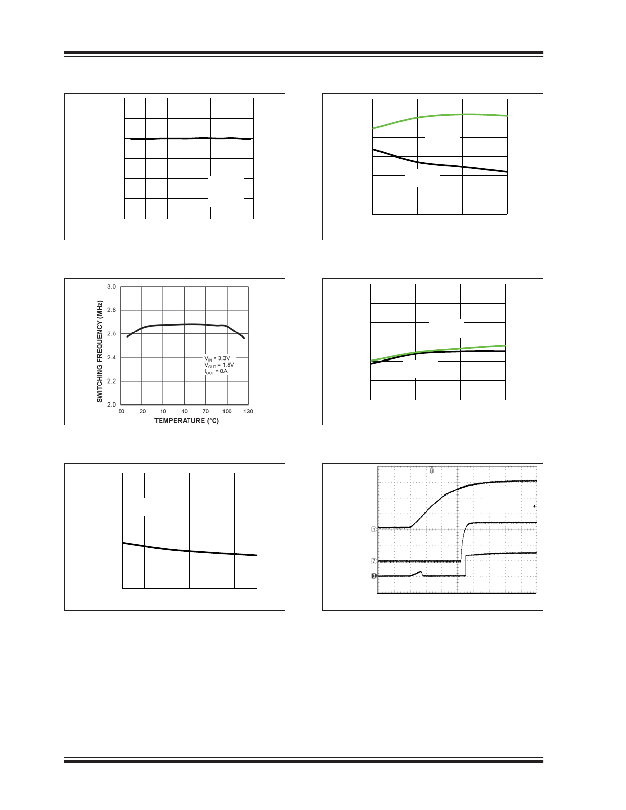
FIGURE 2-13:
Feedback Voltage vs.
Temperature.
FIGURE 2-14:
Switching Frequency vs.
Temperature.
FIGURE 2-15:
Switching Frequency vs.
Output Current.
FIGURE 2-16:
Switching Frequency vs.
Output Current.
FIGURE 2-17:
Switching Frequency vs.
Output Current.
FIGURE 2-18:
V
IN
Soft Turn-On.
0.605
0.610
0.615
0.620
0.625
0.630
0.635
-50
-20
10
40
70
100
130
FEEDBA
CK VOL
TA
G
E
(V
)
TEMPERATURE (°C)
V
IN
= 3.3V
V
OUT
= 1.8V
I
OUT
= 0A
1.20
1.60
2.00
2.40
2.80
3.20
0.0
0.5
1.0
1.5
2.0
2.5
3.0
SW
ITCHING FREQUENCY
(MHz)
OUTPUT CURRENT (A)
V
IN
= 5.0V
V
OUT
= 3.3V
1.20
1.60
2.00
2.40
2.80
3.20
3.60
0.0
0.5
1.0
1.5
2.0
2.5
3.0
SW
ITCHING FREQUENCY
(MHz)
OUTPUT CURRENT (A)
V
IN
= 5.0V
V
OUT
= 1.8V
V
IN
= 3.3V
V
OUT
= 1.8V
1.20
1.60
2.00
2.40
2.80
3.20
3.60
0.0
0.5
1.0
1.5
2.0
2.5
3.0
SW
ITCHING FREQUENCY
(MHz)
OUTPUT CURRENT (A)
V
IN
= 5.0V
V
OUT
= 1.2V
V
IN
= 3.3V
V
OUT
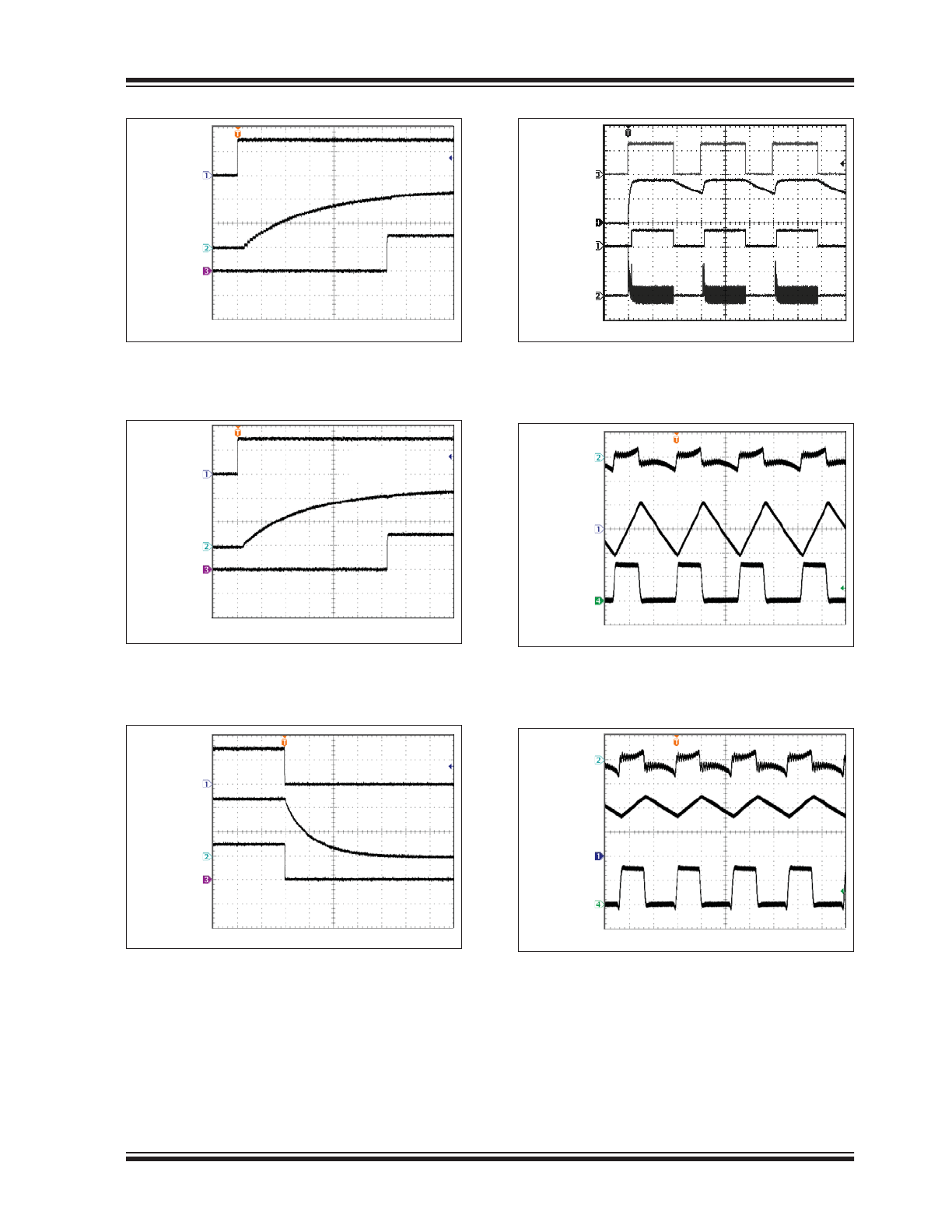
= 1.2V
Time (2ms/div)
V
IN
(1V/div)
V
OUT
(500mV/div)
PG
(2V/div)
V
IN
= 3.0V
V
OUT
= 1.2V
I
OUT
= 0A
2016 Microchip Technology Inc.
DS20005669A-page 9
MIC4930
FIGURE 2-19:
Enable Turn-On (No Load).
FIGURE 2-20:
Enable Turn-On (1A Load).
FIGURE 2-21:
Enable Turn-Off (1A Load).
FIGURE 2-22:
1.4V Pre-Bias Start-Up (EN
Rising).
FIGURE 2-23:
Switching Waveforms
(I
OUT
= 0A).
FIGURE 2-24:
Switching Waveforms
(I
OUT
= 1A).
Time (2ms/div)
EN
(2V/div)
V
OUT
(500mV/div)
PG
(2V/div)
V
IN
= 3.0V
V
OUT
= 1.2V
I
OUT
= 0A
Time (100μs/div)
EN
(2V/div)
V
OUT
(500mV/div)
PG
(2V/div)
V
IN
= 3.0V
V
OUT
= 1.2V
I
OUT
= 1A
Time (100μs/div)
EN
(2V/div)
V
OUT
(500mV/div)
PG
(2V/div)
V
IN
= 3.0V
V
OUT
= 1.2V
I
OUT
= 1A
Time (4ms/div)
EN
(2V/div)
V
OUT
(1V/div)
PG
(1V/div)
I
L
(500mA/div)
Time (200ns/div)
V
OUT RIPPLE
(10mV/div)
SW Node
(2V/div)
I
L
(200mA/div)
V
IN
= 3.0V
V
OUT
= 1.2V (AC-Coupled)
I
OUT
= 0A
Time (200ns/div)
V
OUT
(10mV/div)
SW Node
(2V/div)
I
L
(500mA/div)
V
IN
= 3.0V
V
OUT
= 1.2V (AC-Coupled)
I
OUT
= 1A
MIC4930
DS20005669A-page 10
2016 Microchip Technology Inc.
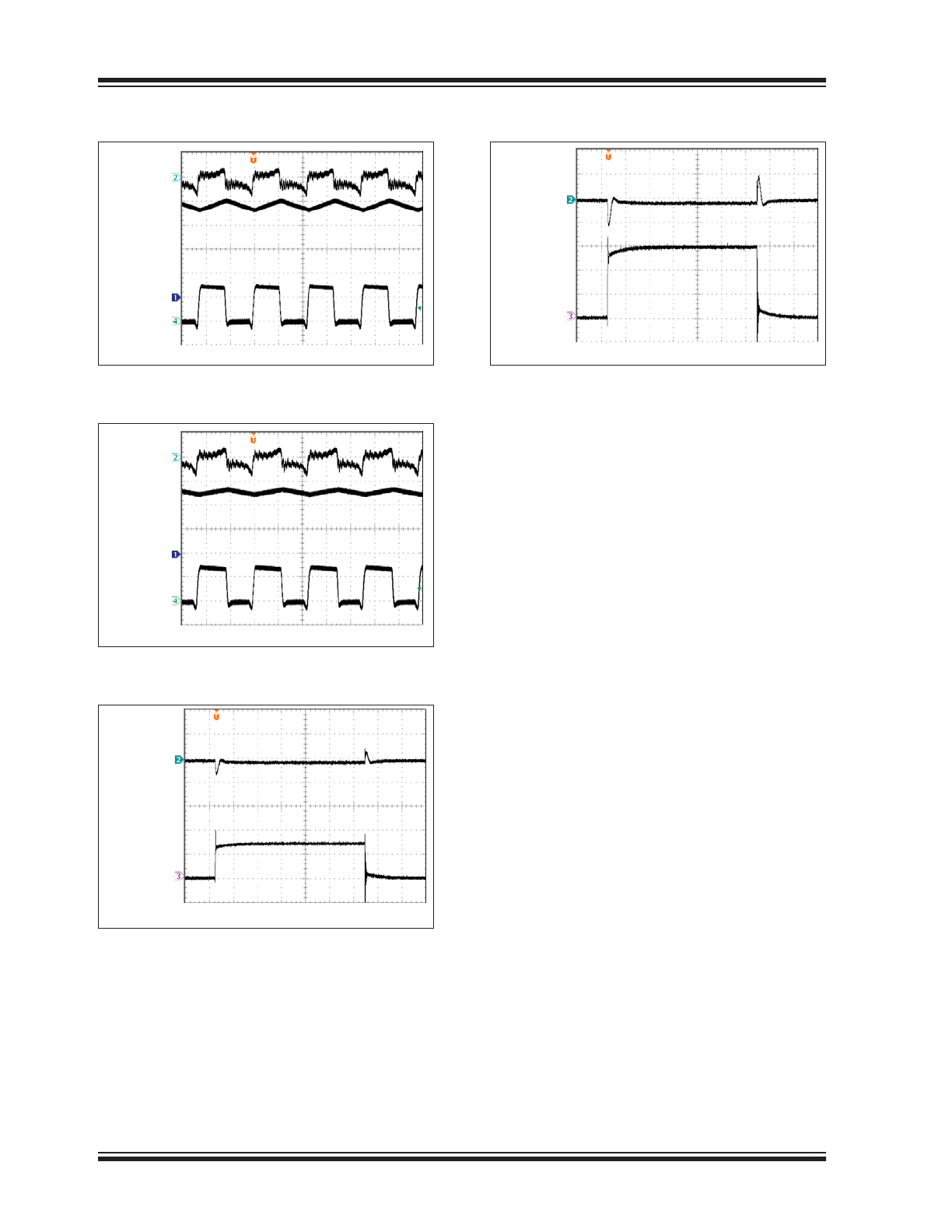
FIGURE 2-25:
Switching Waveforms
(I
OUT
= 3A).
FIGURE 2-26:
Switching Waveforms
(Current Limit).
FIGURE 2-27:
Load Transient Response
(I
OUT
= 1.5A).
FIGURE 2-28:
Load Transient Response
(I
OUT
= 3A).
Time (200ns/div)
V
OUT
(10mV/div)
SW Node
(2V/div)
I
L
(1A/div)
V
IN
= 3.0V
V
OUT
= 1.2V (AC-Coupled)
I
OUT
= 3A
Time (200ns/div)
V
OUT
(10mV/div)
SW Node
(2V/div)
I
L
(2A/div)
V
IN
= 3.0V
V
OUT
= 1.2V (AC-Coupled)
R
LOAD
= 0.25Ω
Time (20μs/div)
V
OUT
(200mV/div)
I
OUT
(1A/div)
V
IN
= 3.0V
V
OUT
= 1.2V (AC-Coupled)
C
OUT
= 10μF
Time (20μs/div)
V
OUT
(200mV/div)
I
OUT
(1A/div)
V
IN
= 3.0V
V
OUT
= 1.2V (AC-Coupled)
C
OUT
= 10μF