
2016 Microchip Technology Inc.
DS20005584A-page 1
MIC4600
Features
• Adjustable Dead Time Circuitry
• Anti-Shoot-Through Protection
• Internal LDO For Single Supply Operation
• Input Voltage Range: 4.5V to 28V
• Fast Propagation Delay – 20 ns
• Up To 1.5 MHz Operation
• Low Voltage Logic Level Inputs For μC or FPGA
Driven Power Solutions
• Independent Inputs For Low and High Side
Drivers
• 2Ω Gate Drive Capable Of Driving 3000 pF Load
With 15 ns Rise and Fall Times
• Low 450 μA Typical Quiescent Current
• 3 mm × 3 mm VQFN Package
• –40
C to +125C Junction Temperature Range
Applications
• Distributed Power Systems
• Communications/Networking Infrastructure
• Set-Top Box, Gateways And Routers
• Printers and Scanners
• μP and FPGA Controlled DC-DC Regulator
General Description
The MIC4600 is a 28V half bridge MOSFET driver
targeted for cost sensitive applications requiring high
performance such as set-top boxes, gateways, routers,
computing peripherals, telecom and networking
equipment.
The MIC4600 operates over a supply range of 4.5V to
28V. It has an internal linear regulator which provides a
regulated 5V to power the MOSFET gate drive and
operates up to 1.5 MHz switching frequency.
The MIC4600 uses an adjustable dead time circuit to
prevent shoot-through in the external high and low-side
MOSFETs.
The MIC4600 is available in a small 3mm × 3mm VQFN
package with a junction temperature range of –40°C to
125°C.
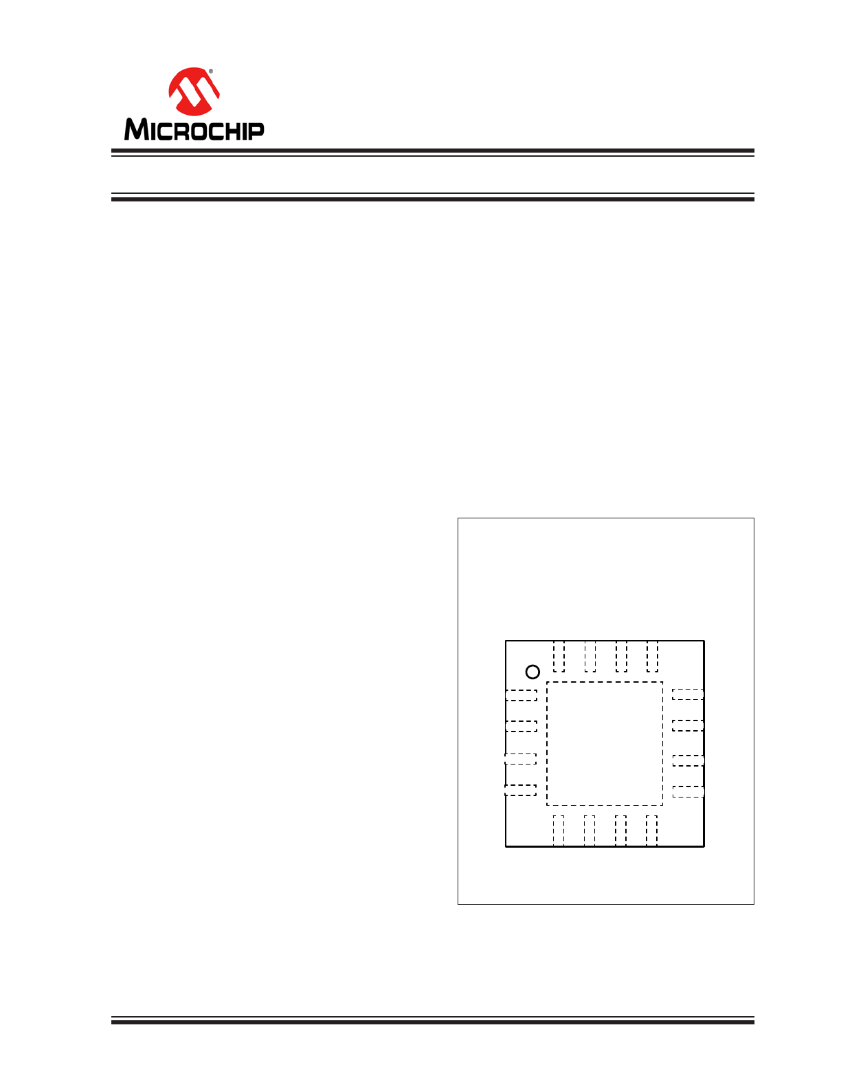
Package Types
MIC4600
3x3 VQFN
Top View
VIN
HSI
DL
PGND
EN
DH
SW
LSI
AGND
AVDD
VDD
BST
AGND
DELAY
FAULT
NC
EPAD
1
2
3
4
12
11
10
9
16
15
14
13
5
6
7
8
28V Half-Bridge MOSFET Driver
MIC4600
DS20005584A-page 2
2016 Microchip Technology Inc.
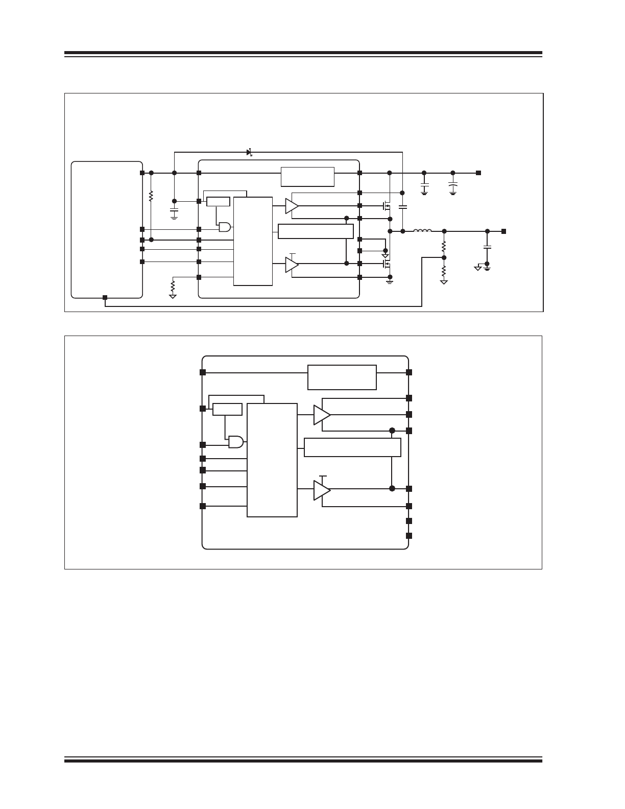
Typical Application Circuit
Functional Block Diagram
MIC4600
3x3 VQFN
+
CONTROLLER
VDD
VDD
AVDD
EN
FAULT
HSI
LSI
EN
FAULT
HSI
LSI
UVLO
D1
MIC4600
LINEAR
REGULATOR
VIN
BST
SW
AGND
AGND
DH
DL
DELAY
ANTI-SHOOT THRU
VDD
PGND
V
IN
4.5V TO 28V
4.7µF
0.1µF
C
BST
33µF
Lo
4.0µH
V
OUT
3.3V/10A
R1
10K
R2
3.24K
100µF
CONTROL
LOGIC
TIMER
1.0µF
105K
FB
100K
EN
FAULT
HSI
LSI
UVLO
MIC4600
LINEAR
REGULATOR
VIN
BST
SW
AGND
AGND
DH
DL
DELAY
ANTI-SHOOT THRU
VDD
PGND
CONTROL
LOGIC
TIMER
AVDD
VDD
2016 Microchip Technology Inc.
DS20005584A-page 3
MIC4600
1.0
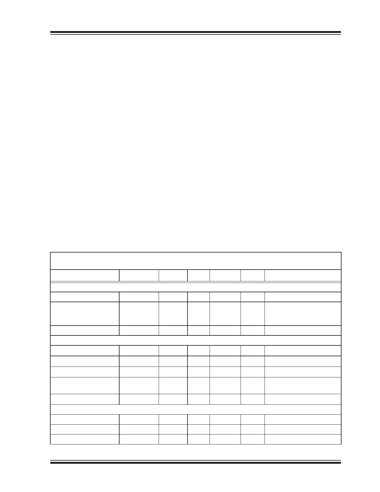
ELECTRICAL CHARACTERISTICS
Absolute Maximum Ratings †
V
IN
to PGND .............................................................................................................................................. –0.3V to +29V
V
DD
to PGND ............................................................................................................................................... –0.3V to +6V
V
SW
to PGND................................................................................................................................... –0.3V to (V
IN
+0.3V)
V
BST
to V
SW
................................................................................................................................................. –0.3V to +6V
V
BST
to PGND............................................................................................................................................ –0.3V to +34V
V
HSI,
V
LSI
to PGND ......................................................................................................................... –0.3V to (V
DD
+0.3V)
V
FAULT
to AGND........................................................................................................................................... –0.3V to +6V
V
EN
to PGND ................................................................................................................................... –0.3V to (V
IN
+0.3V)
PGND to AGND......................................................................................................................................... –0.3V to +0.3V
ESD Protection On All Pins ......................................................................................................... ±2 kV HBM, ±200V MM
Operating Ratings ††
Supply Voltage, V
IN
.................................................................................................................................... +4.5V to +28V
VDD Supply Voltage, V
DD
......................................................................................................................... +4.5V to +5.5V
Enable Input, V
EN
............................................................................................................................................... 0V to V
IN
Maximum Power Dissipation................................................................................................................................ (
Note 1
)
†
Notice: Exceeding the absolute maximum ratings may damage the device.
††
Notice: The device is not guaranteed to function outside its operating ratings.
Note 1:
Specification for packaged product only.
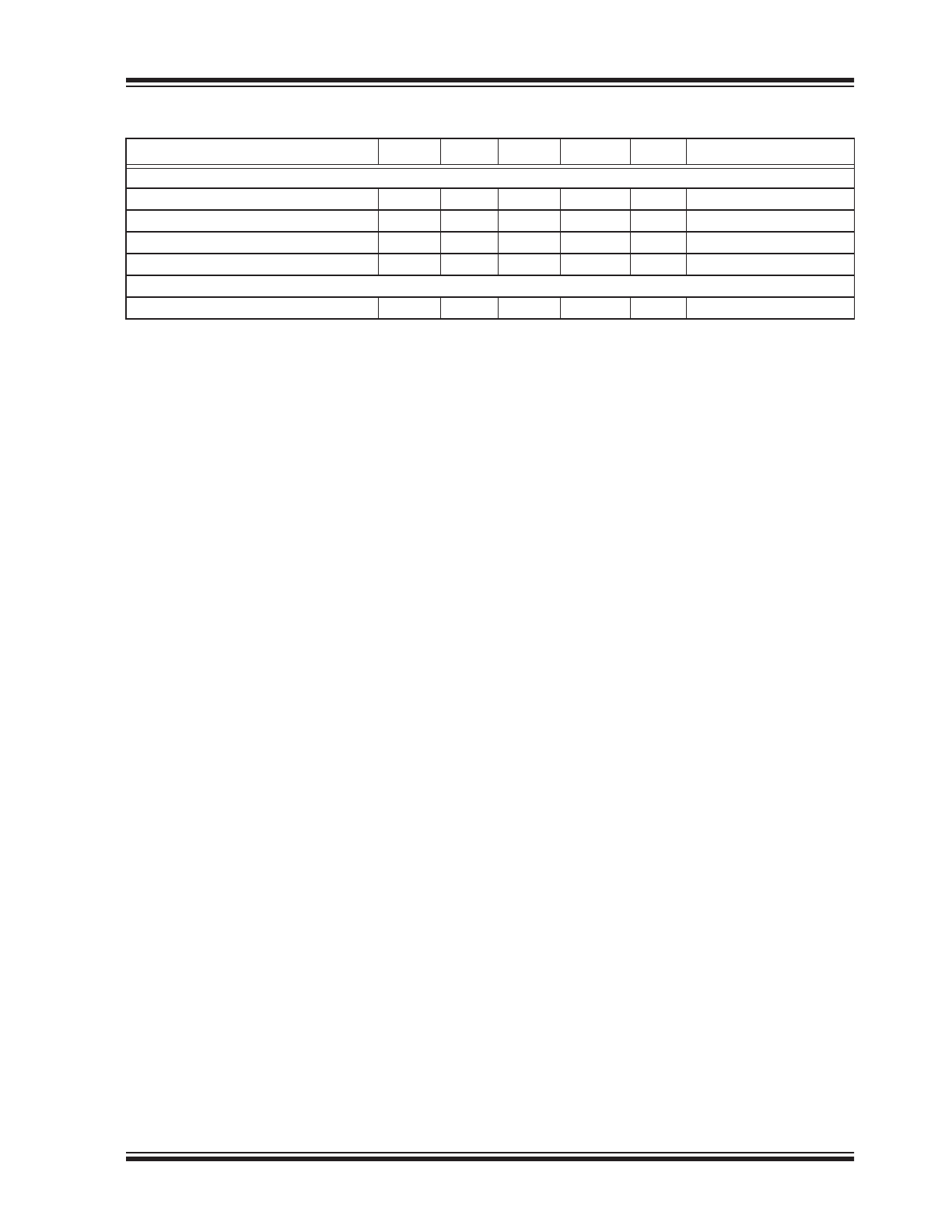
DC CHARACTERISTICS
Electrical Characteristics:
Unless otherwise indicated, V
IN
= V
EN
= 12V, V
BST
– V
SW
= 5V; T
A
= 25°C,
C
VIN
= C
VDD
= 1 μF. Bold values indicate –40°C ≤ T
J
≤
+125°C.
Parameters
Sym.
Min.
Typ.
Max.
Units
Conditions
Power Supply Input
Input Voltage Range (V
IN
)
4.5
—
28
V
—
Quiescent Supply Current
—
450
750
μA
HSI = V
DD
, LSI = 0V,
R
DELAY
= 124 kΩ,
non-switching
Shutdown Supply Current
—
9
20
μA
V
EN
= 0V
V
DD
Supply Voltage
V
DD
Output Voltage
4.8
5
5.4
V
V
IN
= 7V to 26V, I
DD
= 25 mA
V
DD
UVLO Threshold
3.6
4.2
4.3
V
V
DD
Rising
V
DD
UVLO Hysteresis
—
400
—
mV
—
Dropout Voltage
(V
IN
– V
DD
)
—
380
—
mV
I
DD
= 25 mA, V
IN
= 5V
V
DD
Load Regulation
—
1.23
—
%
I
DD
= 0 to 25 mA
Enable Control
EN Logic Threshold
0.65
1.25
1.4
V
Rising
EN Hysteresis
—
69
—
mV
—
EN Input Bias Current
—
—
2
μA
V
EN
= 12V
Note 1:
Specified for packaged product only.
MIC4600
DS20005584A-page 4
2016 Microchip Technology Inc.
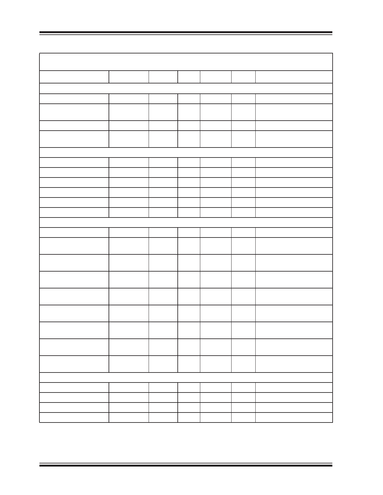
Fault
Fault Over Temperature
—
150
—
°C
T
J
Rising
Over Temperature
Hysteresis
—
23
—
°C
—
FAULT Logic Level Low
—
0.05
0.2
V
I
FAULT
= 5 mA
FAULT Pin Leakage
Current
—
0.01
0.1
μA
V
FAULT
= 5.5V
Input Control
HSI Logic Level High
1.4
—
—
V
—
HSI Logic Level Low
—
—
0.65
V
—
HSI Bias Current
—
0.01
0.1
μA
V
HSI
= 5V
LSI Logic Level High
1.4
—
—
V
—
LSI Logic Level Low
—
—
0.65
V
—
LSI Bias Current
—
0.01
0.1
μA
V
LSI
= 5V
Timing
Dead Time
—
18.7
—
ns
R
DELAY
= 105 kΩ
Switching Frequency
Range
—
1.5
MHz
—
Minimum Allowable Pulse
Width
—
32
—
ns
—
Rise Time (DH, DL)
—
15
—
ns
C
LOAD
= 3 nF, 10%V
DD
to
90%V
DD
Fall Time (DH,DL)
—
13.5
—
ns
C
LOAD
= 3 nF, 90%V
DD
to
10%V
DD
Propagation Delay,
Rising HSI to DH
—
26
—
ns
GND to 10%xV
DD
Propagation Delay,
Rising LSI to DL
—
18
—
ns
GND to 10%xV
DD
Propagation Delay,
Falling HSI to DH
—
55
—
ns
V
DD
to 90%xV
DD
Propagation Delay,
Falling LSI to DL
—
14
—
ns
V
DD
to 90%xV
DD
MOSFET Drivers
DH R
DS(ON)
, High
—
2
3
Ω
I
DH
= 20 mA
DH R
DS(ON)
, Low
—
1.5
3
Ω
I
DH
= –20 mA
DL R
DS(ON)
, High
—
2
3
Ω
I
DL
= 20 mA
DL R
DS(ON)
, Low
—
1
2
Ω
I
DL
= –20 mA
DC CHARACTERISTICS (CONTINUED)
Electrical Characteristics:
Unless otherwise indicated, V
IN
= V
EN
= 12V, V
BST
– V
SW
= 5V; T
A
= 25°C,
C
VIN
= C
VDD
= 1 μF. Bold values indicate –40°C ≤ T
J
≤
+125°C.
Parameters
Sym.
Min.
Typ.
Max.
Units
Conditions
Note 1:
Specified for packaged product only.
2016 Microchip Technology Inc.
DS20005584A-page 5
MIC4600
TEMPERATURE SPECIFICATIONS (
Note 1
)
Parameters
Sym.
Min.
Typ.
Max.
Units
Conditions
Temperature Ranges
Junction Temperature
T
J
—
+150
—
°C
—
Lead Temperature
—
—
260
—
°C
Soldering, 10sec.
Junction Operating Temperature
T
J
–40
—
+125
°C
—
Storage Temperature Range
T
A
–65
—
+150
°C
—
Package Thermal Resistances
Thermal Resistance, 3 x 3 VQFN-16Ld
JA
—
59
—
°C/W
—
Note 1:
The maximum allowable power dissipation is a function of ambient temperature, the maximum allowable
junction temperature and the thermal resistance from junction to air (i.e., T
A
, T
J
,
JA
). Exceeding the
maximum allowable power dissipation will cause the device operating junction temperature to exceed the
maximum +125°C rating. Sustained junction temperatures above +125°C can impact the device reliability.
MIC4600
DS20005584A-page 6
2016 Microchip Technology Inc.
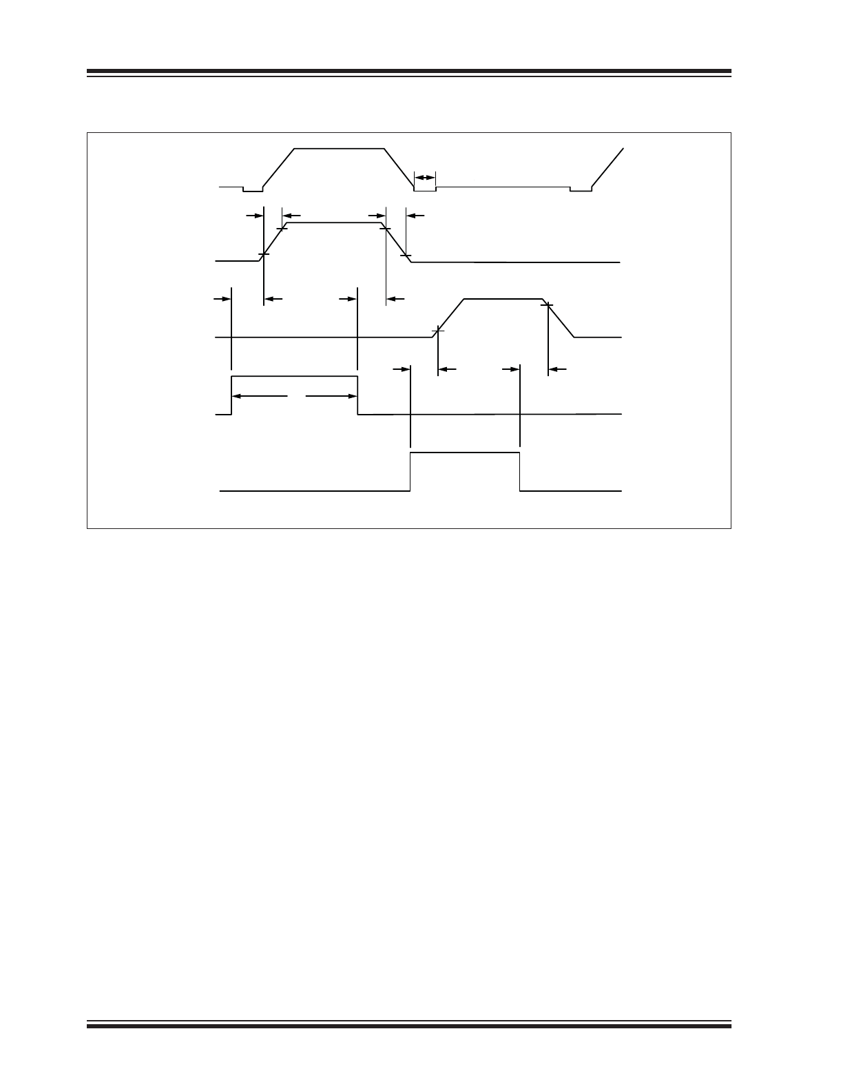
2.0
TIMING DIAGRAM
FIGURE 2-1:
MIC4600 Timing Waveforms.
HS
DH
DL
HSI
LSI
t
DEADTIME
t
R
t
F
90%
90%
10%
10%
10%
t
HPLH
t
HPHL
90%
t
PW
t
LPLH
t
LPHL
2016 Microchip Technology Inc.
DS20005584A-page 7
MIC4600
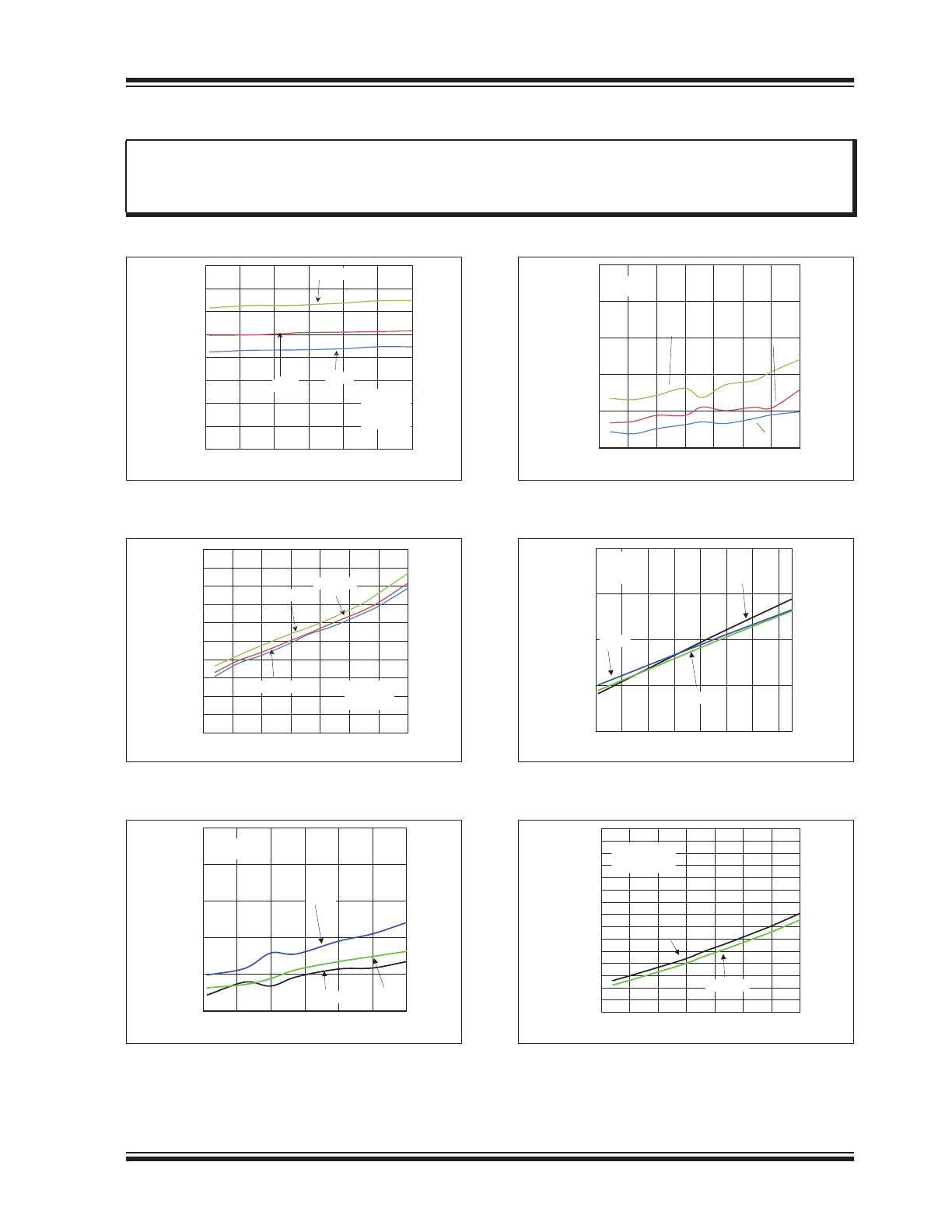
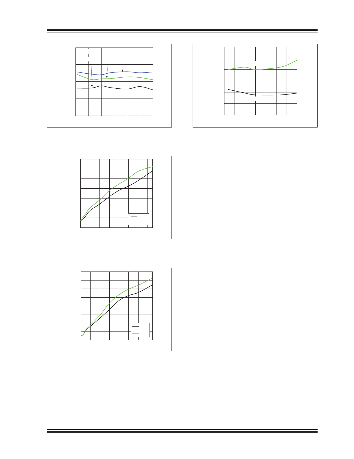
3.0
TYPICAL PERFORMANCE CURVES
NOTE:
Unless otherwise indicated, V
IN
= 12V.
FIGURE 3-1:
VIN Quiescent Current vs.
Input Voltage.
FIGURE 3-2:
VIN Quiescent Current vs.
Temperature.
FIGURE 3-3:
VIN Shutdown Current vs.
Input Voltage.
FIGURE 3-4:
VIN Shutdown Current
vs.Temperature.
FIGURE 3-5:
VIN Operating Current vs.
Frequency.
FIGURE 3-6:
R
DS(ON)
vs. Temperature.
Note:
The graphs and tables provided following this note are a statistical summary based on a limited number of
samples and are provided for informational purposes only. The performance characteristics listed herein
are not tested or guaranteed. In some graphs or tables, the data presented may be outside the specified
operating range (e.g., outside specified power supply range) and therefore outside the warranted range.
200
250
300
350
400
450
500
550
600
4
8
12
16
20
24
28
VIN QUIESCENT
CURRENT
(μA
)
INPUT VOLTAGE (V)
-40°C
25°C
125°C
HSI = VDD
LSI = 0V
SW = 0V
350
370
390
410
430
450
470
490
510
530
550
-50
-25
0
25
50
75
100
125
VIN QUIESCENT
CURRENT
(μA
)
TEMPERATURE (
°C)
V
IN
= 28V
V
IN
= 12V
V
IN
= 4.5V
HSI = VDD
LSI = 0V
SW = 0V
0
10
20
30
40
50
4
8
12
16
20
24
28
VIN SHUTDOW
N
CURRENT
(μA
)
INPUT VOLTAGE (V)
-40ºC
25ºC
125ºC
EN = 0V
SW = 0V
0
10
20
30
40
50
-50
-25
0
25
50
75
100
125
VIN SHUTDOW
N
CURRENT
(μA
)
TEMPERATURE (
°C)
EN = 0V
V
IN
= 4.5V
V
IN
= 12V
V
IN
= 28V
0
0.5
1
1.5
2
0
200
400
600
800 1000 1200 1400
VIN OPERA
T
ING
CURRENT
(mA
)
FREQUENCY (kHz)
-40ºC
25ºC
125ºC
VIN = 12V
SW = 0V
C
LOAD
=0nF
0.6
0.7
0.8
0.9
1
1.1
1.2
1.3
1.4
1.5
1.6
1.7
1.8
1.9
2
2.1
-50
-25
0
25
50
75
100
125
R
DS
(ON)
(Ω
)
TEMPERATURE (°C)
V
IN
= 4.5V
SW = 0V
HSI = LSI = 0V
I
DL
= 50mA
V
IN
= 12V
MIC4600
DS20005584A-page 8
2016 Microchip Technology Inc.
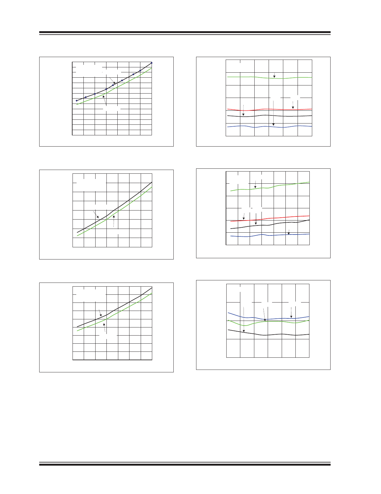
Note:
Unless otherwise indicated, V
IN
= 12V.
FIGURE 3-7:
R
DS(ON)
vs. Temperature.
FIGURE 3-8:
R
DS(ON)
vs. Temperature.
FIGURE 3-9:
R
DS(ON)
vs. Temperature.
.
FIGURE 3-10:
Propagation Delay vs. Input
Voltage.
FIGURE 3-11:
Propagation Delay vs.
Temperature.
FIGURE 3-12:
DH Rise Time vs. Input
Voltage.
0.7
0.8
0.9
1
1.1
1.2
1.3
1.4
1.5
1.6
1.7
1.8
1.9
2
2.1
-50
-25
0
25
50
75
100
125
R
DS
(ON)
(Ω)
TEMPERATURE (°C)
V
IN
= 4.5V
SW = 0V
HSI = LSI = 0V
I
DH
= 50mA
V
IN
= 12V
1.4
1.6
1.8
2
2.2
2.4
2.6
2.8
3
-50
-25
0
25
50
75
100
125
R
DS
(ON)
(Ω)
TEMPERATURE (°C)
V
IN
= 4.5V
SW = 0V
HSI = LSI = VDD
I
DL
= -50mA
V
IN
= 12V
1
1.2
1.4
1.6
1.8
2
2.2
2.4
2.6
2.8
-50
-25
0
25
50
75
100
125
R
DS
(ON)
(Ω)
TEMPERATURE (°C)
V
IN
= 4.5V
SW = 0V
HSI = LSI = VDD
I
DH
= -50mA
V
IN
= 12V
10
20
30
40
50
60
70
4
8
12
16
20
24
28
DELA
Y
(ns)
VIN (V)
t
HPLH
t
HPHL
t
LPLH
TEMP = 25°C
SW = 0V
t
LPHL
10
20
30
40
50
60
70
-50
-25
0
25
50
75
100
125
DELA
Y
(ns)
TEMPERATURE (°C)
t
HPLH
t
HPHL
t
LPLH
VIN = 12V
SW = 0V
t
LPHL
8
10
12
14
16
4
8
12
16
20
24
28
tr (ns
)
VIN (V)
25°C
-40°C
125°C
SW = 0V
2016 Microchip Technology Inc.
DS20005584A-page 9
MIC4600
FIGURE 3-13:
DH Fall Time vs. Input
Voltage.
FIGURE 3-14:
Deadtime vs. R
DELAY
for
DL↓ to DH↑.
FIGURE 3-15:
Deadtime vs. R
DELAY
for
DH↓ to DL↑.
FIGURE 3-16:
Deadtime Delay vs.
Temperature.
8
10
12
14
16
4
8
12
16
20
24
28
tf (ns
)
VIN (V)
25°C
-40°C
125°C
SW = 0V
0
20
40
60
80
100
120
140
0
200
400
600
800 1,000 1,200 1,400
T
DE
A
D
(ns
)
R
DELAY
(kΩ)
4.5Vin
12Vin
0
20
40
60
80
100
120
140
160
0
200
400
600
800 1,000 1,200 1,400
T
DE
A
D
(ns
)
R
DELAY
(kΩ)
4.5Vin
12Vin
80
85
90
95
100
105
110
-50
-25
0
25
50
75
100
125
T
DE
A
D
(ns
)
TEMPERATURE (°C)
DL↓ to DH↑
DH↓ to DL↑
MIC4600
DS20005584A-page 10
2016 Microchip Technology Inc.
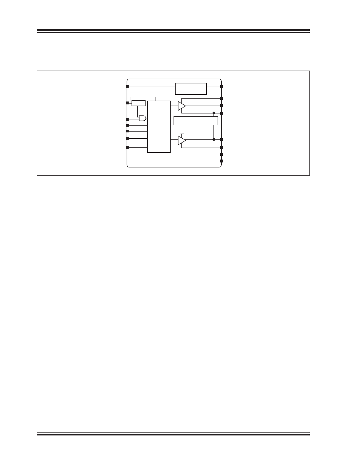
4.0
FUNCTIONAL CHARACTERISTICS
4.1
Functional Diagram
FIGURE 4-1:
Functional Diagram.
4.2
Functional Description
The MIC4600 is a 28V half-bridge MOSFET driver with
integrated LDO. It is designed to independently drive
both high-side and low-side N-Channel MOSFETs. The
LDO eliminates the need for a second VDD supply
voltage by generating the gate drive voltage from the
input supply. The MIC4600 offers a wide 4.5V to 28V
operating supply range. Refer to the MIC4600 Block
Diagram above.
The high and low-side drivers contain an input buffer
with hysteresis and an output buffer. The high-side
output buffer includes a high-speed level-shifting circuit
that is referenced to the HS pin. An external diode is
used to supply V
DD
to the bootstrap circuit that provides
the drive voltage for the high-side output.
4.2.1
STARTUP AND UVLO
The UVLO circuit monitors V
DD
and inhibits both
drivers in a low state when the supply voltage is below
the UVLO threshold. Hysteresis in the UVLO circuit
prevents noise and circuit impedance from causing
chatter during turn-on.
4.2.2
ENABLE INPUT
A logic high on the enable pin (EN) allows normal
operation to occur. Conversely, when a logic low is
applied on the enable pin, the high and low-side driver
outputs turn-off and the driver enters a low supply
current shutdown mode. Do not leave floating.
4.2.3
DEAD-TIME DELAY
Shoot-through occurs in a half-bridge or synchronous
buck topology when both the high and low side
MOSFETs conduct at the same time. This condition is
caused by driver propagation delay variation and
MOSFET turn on/off times. Shoot-through causes an
increase in MOSFET power dissipation, circuit noise
and interference with power circuit operation. A resistor
on the DELAY pin sets the break-before-make delay
time between the high and low-side MOSFETs . See
the Applications section for additional information.
4.2.4
INPUT STAGE
Both the HSI and LSI pins are referenced to the AGND
pin. The voltage state of the input signal does not
change the quiescent current draw of the driver.
The MIC4600 has a TTL-compatible input range and
can be used with input signals with amplitude less than
or equal to the V
DD
voltage. A small amount of
hysteresis improves the noise immunity of the driver
inputs.
4.2.5
LOW-SIDE DRIVER
Figure 4-2
shows a block diagram of the low-side
driver. The low-side driver is designed to drive a ground
(PGND pin) referenced N-channel MOSFET. The
low-side gate drive voltage equals V
DD
, which is
typically 5V.
A low driver impedance allows the external MOSFET to
be turned on and off quickly. The rail-to-rail drive
capability of the output ensures a low R
DSON
from the
external MOSFET.
A high level applied to LSI pin causes the upper driver
MOSFET to turn on and VDD voltage is applied to the
gate of the external MOSFET. A low level on the LSI pin
turns off the upper driver and turns on the low side
driver to ground the gate of the external MOSFET.
EN
FAULT
HSI
LSI
UVLO
MIC4600
LINEAR
REGULATOR
VIN
BST
SW
AGND
AGND
DH
DL
DELAY
ANTI-SHOOT THRU
VDD
PGND
CONTROL
LOGIC
TIMER
AVDD
VDD