
2015 Microchip Technology Inc.
DS20005478A-page 1
MIC45404
Features
• Input Voltage Range: 4.5V to 19V
• Output Current: Up to 5A
• 82% Peak Efficiency at 12 V
IN
, 0.9 V
OUT
• Pin-Selectable Output Voltages: 0.7V, 0.8V, 0.9V,
1.0V, 1.2V, 1.5V, 1.8V, 2.5V, 3.3V
• ±1% Output Voltage Accuracy
• Supports Safe Pre-Biased Start-up
• Pin-Selectable Current Limit
• Pin-Selectable Switching Frequency
• Internal Soft Start
• Thermal Shutdown
• Hiccup Mode Short-Circuit Protection
• Available in a 54-Lead 6 mm x 10 mm QFN
Package
• Ultra-Low Profile: 2.0 mm Height
• -40°C to +125°C Junction Temperature Range
Applications
• Servers, Data Storage, Routers and Base Stations
• FPGAs, DSP and Low-Voltage ASIC Power
General Description
The MIC45404 device is an ultra-low profile, synchro-
nous step-down regulator module, featuring a unique
2.0 mm height. The module incorporates a DC-to-DC
regulator, bootstrap capacitor, high-frequency input
capacitor and an inductor in a single package. The
module pinout is optimized to simplify the Printed
Circuit Board (PCB) layout process.
This highly integrated solution expedites system
design and improves product time to market. The inter-
nal MOSFETs and inductor are optimized to achieve
high efficiency at low output voltage. Due to the fully
optimized design, MIC45404 can deliver up to 5A
current with a wide input voltage range of 4.5V to 19V.
The MIC45404 is available in a 54-lead 6 mm x
10 mm x 2.0 mm
QFN package with a junction operat-
ing temperature range from -40
C to +125C, which
makes an excellent solution for systems in which PCB
real-estate and height are important limiting factors,
and air flow is restricted.
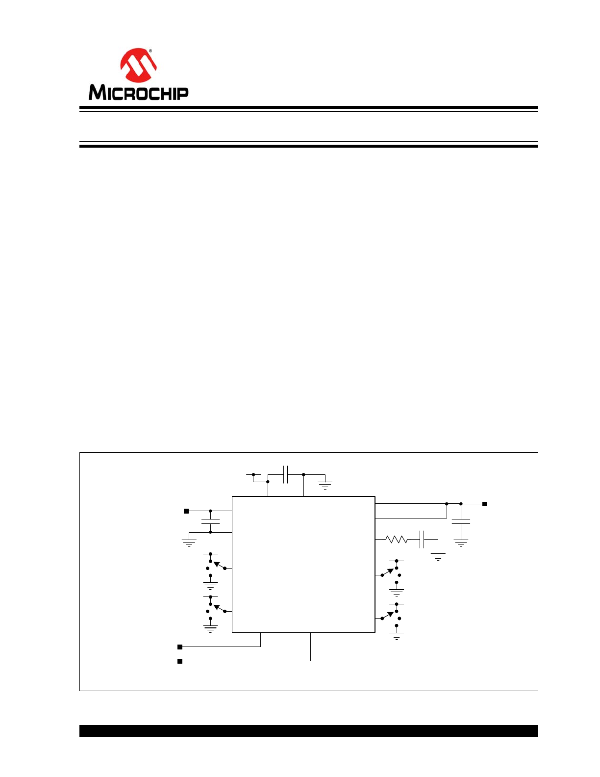
Typical Application
MIC45404 12V 5A DC-to-DC Converter
V
IN
OUT
V
IN
4.5V to 19V
FREQ
V
DDA
VOSET1
PG
GND
GND
VOSET0
COMP
EN/DLY
OUTSNS
MIC45404
V
DDA
Power-Good
Enable
V
DDA
V
DDA
Output
Voltage
Selection
V
DDA
Frequency
Selection
I
LIM
V
DDA
Current Limit
Selection
V
OUT
19V 5A Ultra-Low Profile DC-to-DC Power Module
MIC45404
DS20005478A-page 2
2015 Microchip Technology Inc.
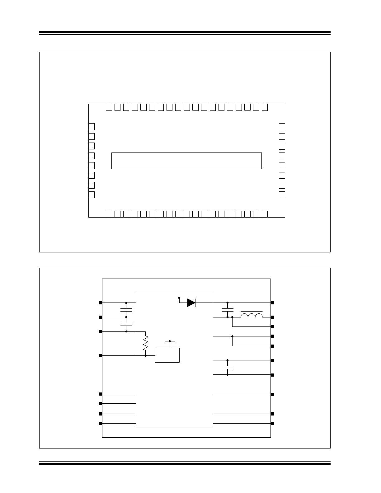
Package Types
Functional Diagram
MIC45404
6 mm x 10 mm QFN*
(Bottom View)
8
26
22
24
23
3
37
35
34
25
47
46
7
KEEPOUT
GND
GND
BS
T
PG
V
DD
A
LX
OUT
GND
21
KEEPOUT
48
38
4
1
2
A
GND
VO
SE
T
1
NC
41
43
53
OUTS
NS
SN
S
33
VO
SE
T
0
LX
44
45
V
DD
P
31
30
29
32
52
36
28
20
9
LX
LX
LX
LX
LX
LX
LX
LX
LX
OUT
OUT
12
OUT
13
OUT
14
OUT
15
OUT
16
OUT
17
OUT
18
OUT
19
GND
V
IN
V
IN
27
LX
LX
39
40
LX
KE
EP
OU
T
BS
T
4
2
NC
I
LIM
49 FREQ
50
51 GND
COMP
54 OUTSNS
KE
EP
OU
T
10
OUT
11
6
GND_E
X
T
5
GND_E
X
T
MIC45404YMP
GND_EP
* Includes Exposed Thermal Pad (EP); see
Table 3-1
.
LX
BST
I
LIM
FREQ
V
DDA
VOSET1
PG
AGND
VOSET0
COMP
EN/DLY
OUTSNS
V
IN
P
GND
V
DDP
PWM
Regulator
100 nF
47 pF
LX
BST
VOSET1
A
GND
VOSET0
GND_EP
OUTSNS
GND
COMP
OUT
I
LIM
FREQ
V
DDA
PG
EN/DLY
V
IN
V
DDP
GND_EXT
V
DDP
LDO
V
IN

2015 Microchip Technology Inc.
DS20005478A-page 3
MIC45404
1.0
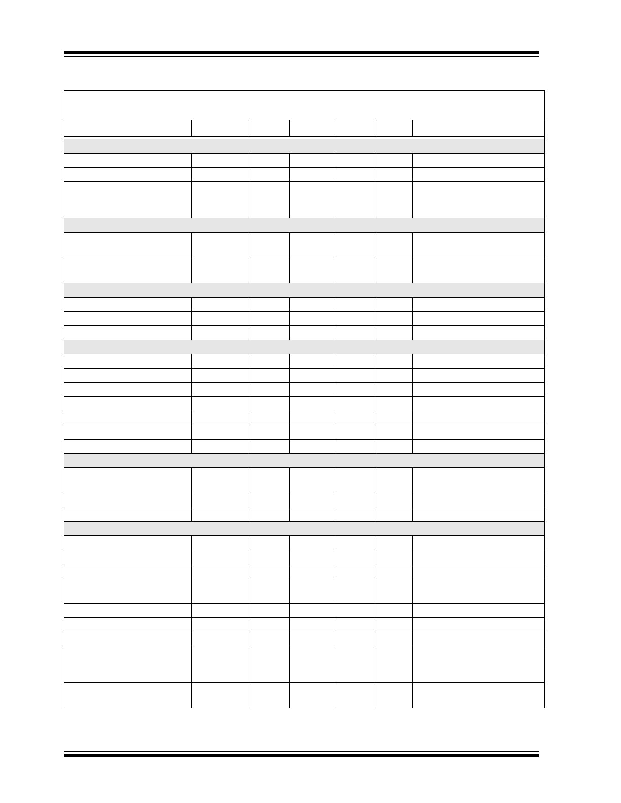
ELECTRICAL CHARACTERISTICS
Absolute Maximum Ratings†
V
IN
to A
GND
................................................................................................................................................ -0.3V to +20V
V
DDP
, V
DDA
to A
GND
..................................................................................................................................... -0.3V to +6V
V
DDP
to V
DDA
............................................................................................................................................ -0.3V to +0.3V
VOSETX, FREQ, I
LIM
, to A
GND
.................................................................................................................... -0.3V to +6V
BST to LX..................................................................................................................................................... -0.3V to +6V
BST to A
GND
.............................................................................................................................................. -0.3V to +26V
EN/DLY to A
GND
...................................................................................................................... -0.3V to V
DDA
+ 0.3V, +6V
PG to A
GND
.................................................................................................................................................. -0.3V to +6V
COMP, OUTSNS to A
GND
....................................................................................................... -0.3V to V
DDA
+ 0.3V, +6V
A
GND
to GND ............................................................................................................................................ -0.3V to +0.3V
Junction Temperature .......................................................................................................................................... +150°C
Storage Temperature (T
S
) ...................................................................................................................... -65°C to +150°C
Lead Temperature (soldering, 10s) ........................................................................................................................ 260°C
ESD Rating
(
1
)
HBM ........................................................................................................................................................................... 2kV
MM ........................................................................................................................................................................... 150V
CDM ....................................................................................................................................................................... 1500V
Note 1:
Devices are ESD-sensitive. Handling precautions are recommended. Human body model, 1.5 k
in series
with 100 pF.
Operating Ratings
(
1
)
Supply Voltage (V
IN
) ..................................................................................................................................... 4.5V to 19V
Externally Applied Analog and Drivers Supply Voltage (V
IN
= V
DDA
= V
DDP
) .............................................. 4.5V to 5.5V
Enable Voltage (EN/DLY)............................................................................................................................... 0V to V
DDA
Power Good (PG) Pull-up Voltage (VPU_PG) ................................................................................................ 0V to 5.5V
Output Current ............................................................................................................................................................. 5A
Junction Temperature (T
J
) ..................................................................................................................... -40°C to +125°C
Note 1:
The device is not ensured to function outside the operating range.
†
Notice:
Stresses above those listed under “Maximum Ratings” may cause permanent damage to the device. This is
a stress rating only and functional operation of the device at those or any other conditions above those indicated in
the operational sections of this specification is not intended. Exposure to maximum rating conditions for extended
periods may affect device reliability.
MIC45404
DS20005478A-page 4
2015 Microchip Technology Inc.
ELECTRICAL CHARACTERISTICS
(
1
)
Electrical Specifications:
unless otherwise specified, V
IN
= 12V; C
VDDA
= 2.2 µF, T
A
= +25°C.
Boldface
values indicate -40°C
T
J
+125°C.
Parameter
Symbol
Min.
Typ.
Max.
Units
Test Conditions
V
IN
Supply
Input Range
V
IN
4.5
—
19
V
Disable Current
I
VINQ
—
33
60
µA
EN/DLY = 0V
Operating Current
I
VINOp
—
5.35
8.5
mA
EN/DLY > 1.28V,
OUTSNS = 1.15 x V
OUT(NOM)
,
no switching
V
DDA
5V Supply
Operating Voltage
V
DDA
4.8
5.1
5.4
V
EN/DLY > 0.58V,
I
VDDA
= 0 mA to 10 mA
Dropout Operation
3.6
3.75
—
V
V
IN
= 4.5V, EN/DLY > 0.58V,
I
VDDA
= 10 mA
V
DDA
Undervoltage Lockout
V
DDA
UVLO Rising
UVLO_R
3.1
3.5
3.9
V
V
DDA
Rising, EN/DLY > 1.28V
V
DDA
UVLO Falling
UVLO_F
2.87
3.2
3.45
V
V
DDA
Falling, EN/DLY > 1.28V
V
DDA
UVLO Hysteresis
UVLO_H
—
300
—
mV
EN/DLY Control
LDO Enable Threshold
EN_LDO_R
—
515
600
mV
Turns on V
DDA
LDO
LDO Disable Threshold
EN_LDO_F
450
485
—
mV
Turns off V
DDA
LDO
LDO Threshold Hysteresis
EN_LDO_H
—
30
—
mV
EN/DLY Rising Threshold
EN_R
1.14
1.21
1.28
V
Initiates power stage operation
EN/DLY Falling Threshold
EN_F
—
1.06
—
V
Stops power stage operation
EN/DLY Hysteresis
EN_H
—
150
—
mV
EN/DLY Pull-up Current
EN_I
1
2
3
µA
Switching Frequency
Programmable
Frequency (High Z)
f
SZ
360
400
440
kHz
FREQ = High Z (open)
Programmable Frequency 0
f
S0
500
565
630
kHz
FREQ= Low (GND)
Programmable Frequency 1
f
S1
700
790
880
kHz
FREQ = High (V
DDA
)
Overcurrent Protection
HS Current Limit 0
I
LIM_HS0
6.0
7.1
8.1
A
I
LIM
= Low (GND)
HS Current Limit 1
I
LIM_HS1
8.1
9.3
10.3
A
I
LIM
= High (V
DDA
)
HS Current Limit High Z
I
LIM_HSZ
9.3
10.5
11.9
A
I
LIM
= High Z (open)
Top FET Current Limit
Leading-Edge Blanking Time
LEB
—
108
—
ns
LS Current Limit 0
I
LIM_LS0
3.0
4.6
6.3
A
I
LIM
= Low (GND)
LS Current Limit 1
I
LIM_LS1
4.0
6.2
7.9
A
I
LIM
= High (V
DDA
)
LS Current Limit High Z
I
LIM_LSZ
5.0
6.8
8.6
A
I
LIM
= High Z (Open)
OC Events Count for Hiccup
IN
HICC_DE
—
15
—
Clock
Cycles
Number of subsequent cycles
in current limit before entering
hiccup overload protection
Hiccup Wait Time
t
HICC_WAIT
—
3 x Soft
Start Time
—
Duration of the High Z state on
LX before new soft start.
Note 1:
Specification for packaged product only.
2015 Microchip Technology Inc.
DS20005478A-page 5
MIC45404
Pulse-Width Modulation (PWM)
Minimum LX On Time
T
ON(MIN)
—
26
—
ns
T
A
= T
J
= +25°C
Minimum LX Off time
T
OFF(MIN)
90
135
190
ns
V
IN
= V
DDA
= 5V, OUTSNS = 3V,
FREQ = Open (400 kHz setting),
VOSET0 = VOSET1 = 0V
(3.3V setting),
T
A
= T
J
= +25°C
Minimum Duty Cycle
D
MIN
—
0
—
%
OUTSNS > 1.1 x V
OUT(NOM)
Gm Error Amplifier
Error Amplifier
Transconductance
Gm
EA
—
1.4
—
mS
Error Amplifier DC Gain
A
EA
—
50000
—
V/V
Error Amplifier Source/Sink
Current
I
SR_SNK
-400
—
+400
µA
T
A
= T
J
= +25°C
COMP Output Swing High
COMP_H
—
2.5
—
V
COMP Output Swing Low
COMP_L
—
0.8
—
V
COMP-to-Inductor Current
Transconductance
Gm
PS
—
12.5
—
A/V
V
OUT
= 1.2V, I
OUT
= 4A
Output Voltage DC Accuracy
Output Voltage Accuracy for
Ranges 1 and 2
OutErr12
-1
—
1
%
4.75V
V
IN
19V,
V
OUT
= 0.7V to 1.8V,
T
A
= T
J
= -40°C to +125°C,
I
OUT
= 0A
Output Voltage Accuracy for
Range 3
OutErr3
-1.5
—
1.5
%
4.75V
V
IN
19V,
V
OUT
= 2.49V to 3.3V,
T
A
= T
J
= -40°C to +125°C,
I
OUT
= 0A
Load Regulation
LoadReg
—
0.03
—
%
I
OUT
= 0A to 5A
Line Regulation
LineReg
—
0.01
—
%
6V < V
IN
< 19V, I
OUT
= 2A
Internal Soft Start
Reference Soft Start
Slew Rate
SS_SR
—
0.42
—
V/ms V
OUT
= 0.7V, 0.8V, 0.9V,
1.0V, 1.2V
Power Good (PG)
PG Low Voltage
PG_V
OL
—
0.17
0.4
V
I
PG
= 4 mA
PG Leakage Current
PG_I
LEAK
-1
0.02
1
µA
PG = 5V
PG Rise Threshold
PG_R
90
92
95
%
V
OUT
Rising
PG Fall Threshold
PG_F
87.5
90
92.5
%
V
OUT
Falling
PG Rise Delay
PG_R_DLY
—
0.45
—
ms
V
OUT
Rising
PG Fall Delay
PG_F_DLY
—
80
—
µs
V
OUT
Falling
ELECTRICAL CHARACTERISTICS
(
1
)
(CONTINUED)
Electrical Specifications:
unless otherwise specified, V
IN
= 12V; C
VDDA
= 2.2 µF, T
A
= +25°C.
Boldface
values indicate -40°C
T
J
+125°C.
Parameter
Symbol
Min.
Typ.
Max.
Units
Test Conditions
Note 1:
Specification for packaged product only.
MIC45404
DS20005478A-page 6
2015 Microchip Technology Inc.
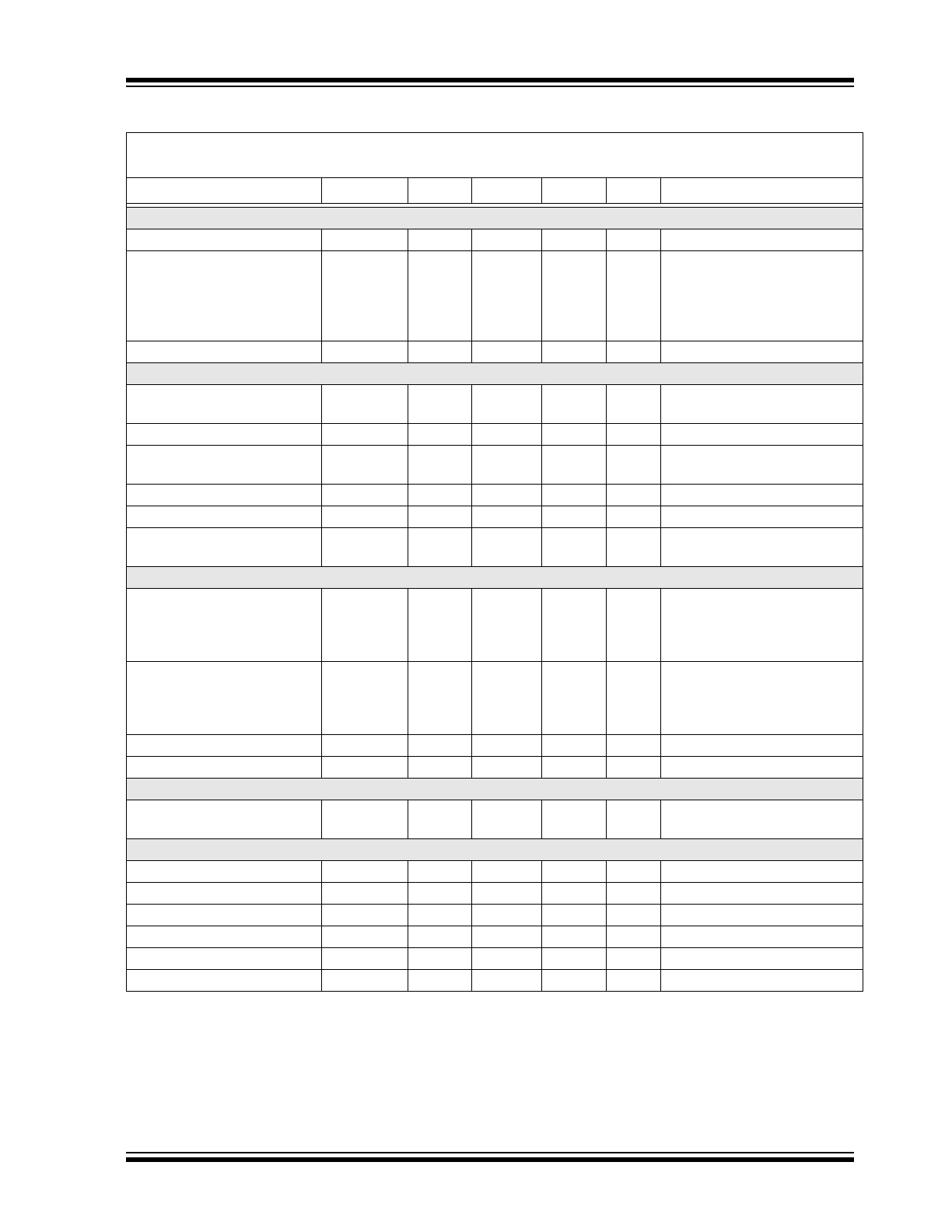
Thermal Shutdown
Thermal Shutdown
T
SHDN
—
160
—
°C
Thermal Shutdown
Hysteresis
T
SHDN_HYST
—
25
—
°C
Efficiency
Efficiency
η
—
82
—
%
V
IN
= 12V, V
OUT
= 0.9V,
I
OUT
= 2A, f
S
= f
SZ
= 400 kHz,
T
A
= +25°C
ELECTRICAL CHARACTERISTICS
(
1
)
(CONTINUED)
Electrical Specifications:
unless otherwise specified, V
IN
= 12V; C
VDDA
= 2.2 µF, T
A
= +25°C.
Boldface
values indicate -40°C
T
J
+125°C.
Parameter
Symbol
Min.
Typ.
Max.
Units
Test Conditions
Note 1:
Specification for packaged product only.
TEMPERATURE SPECIFICATIONS
Electrical Specifications:
unless otherwise specified, V
IN
= 12V; C
VDDA
= 2.2 µF, T
A
= +25°C.
Boldface
values indicate -40°C
T
J
+125°C.
Parameters
Sym.
Min.
Typ.
Max.
Units
Conditions
Temperature Ranges
Operating Ambient Junction Range
T
J
-40
—
+125
°C
Storage Temperature Range
T
A
-65
—
+150
°C
Maximum Junction Temperature
T
J
-40
—
+150
°C
Package Thermal Resistances
Thermal Resistance, 54 Lead,
6 mm x10 mm QFN
JA
—
20
—
°C/W
See “MIC45404 Evaluation
Board User’s Guide”
2015 Microchip Technology Inc.
DS20005478A-page 7
MIC45404
2.0
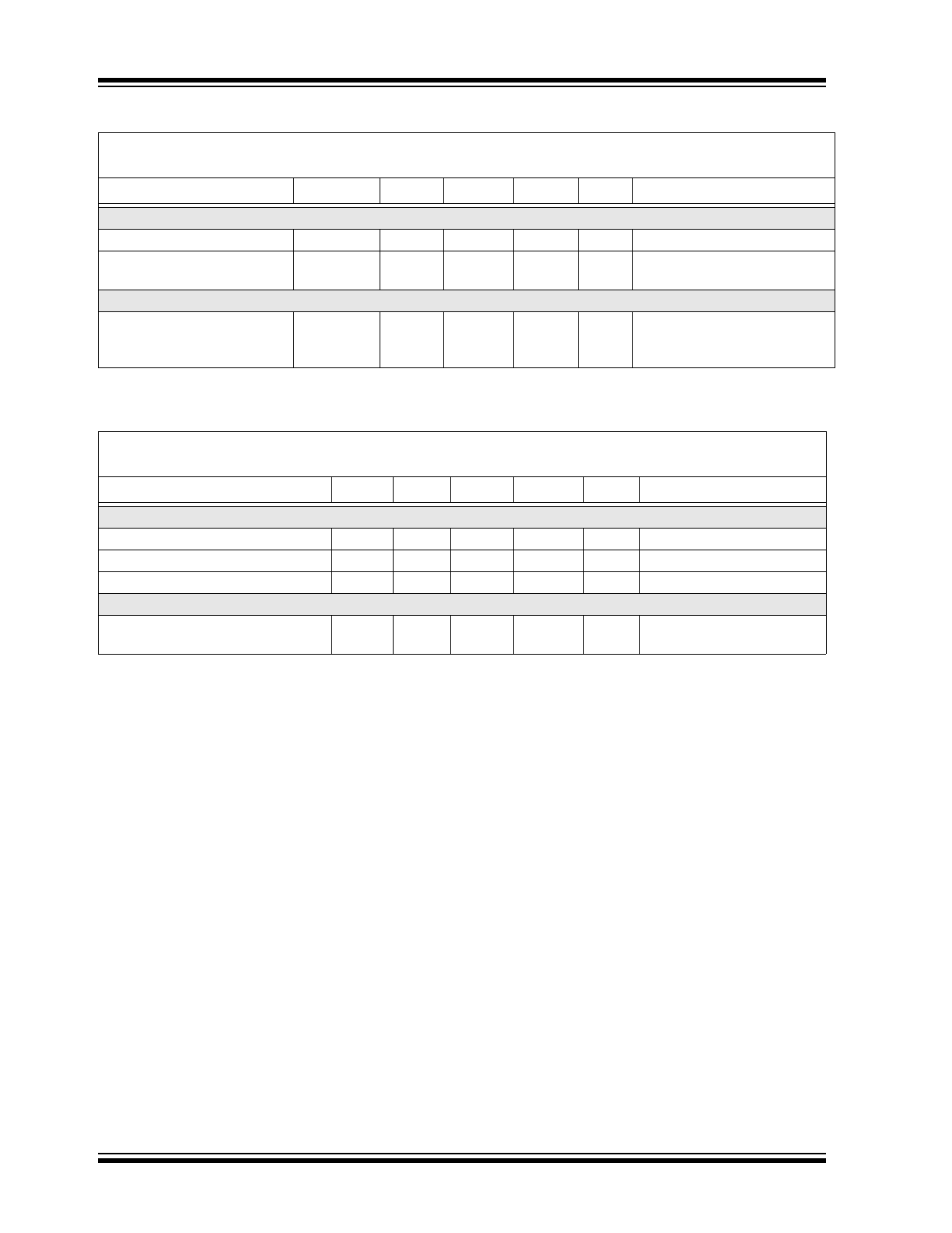
TYPICAL PERFORMANCE CURVES
Note:
Unless otherwise indicated, V
IN
= 12V; C
VDDA
= 2.2 µF, T
A
= +25°C.
FIGURE 2-1:
Operating Current (IQ) vs.
Input Voltage.
FIGURE 2-2:
V
DDA
Voltage vs. Input
Voltage.
FIGURE 2-3:
Output Current Limit vs.
Input Voltage.
FIGURE 2-4:
Enable Threshold vs. Input
Voltage.
FIGURE 2-5:
EN/DLY Pull-up Current vs.
Input Voltage.
FIGURE 2-6:
Operating Current (IQ) vs.
Temperature.
Note:
The graphs and tables provided following this note are a statistical summary based on a limited number of
samples and are provided for informational purposes only. The performance characteristics listed herein
are not tested or guaranteed. In some graphs or tables, the data presented may be outside the specified
operating range (e.g., outside specified power supply range) and therefore outside the warranted range.
15.00
17.00
19.00
21.00
23.00
25.00
27.00
29.00
31.00
33.00
35.00
4
6
8
10
12
14
16
18
20
IQ (mA
)
V
IN
(V)
f = 565 kHz
V
OUT
= 1.8V
f = 400 kHz
V
OUT
= 1.0V
Switching
I
OUT
= 0A
f = 790 kHz
V
OUT
= 3.3V
4
4.2
4.4
4.6
4.8
5
5.2
4.5
6.5
8.5
10.5
12.5
14.5
16.5
18.5
V
DD
A
(V)
V
IN
(V)
IoutSet 0
IoutSet 0.01
I
VDDA
= 0 mA
I
VDDA
= 10 mA
5
5.5
6
6.5
7
7.5
8
8.5
4.5
5
5.5
6
8
10
12
14
16
18
19
I
OUT
(A
)
V
IN
(V)
I
LIM
= GND
I
LIM
= V
DDA
I
LIM
= high Z
V
OUT
= 1.2V
f = 400 kHz
0.9
0.95
1
1.05
1.1
1.15
1.2
1.25
1.3
4.5
6.5
8.5
10.5
12.5
14.5
16.5
18.5
Enable (V)
V
IN
(V)
Enable rising
Enable falling
1
1.2
1.4
1.6
1.8
2
2.2
2.4
2.6
2.8
3
4
5
6
7
8
9 10 11 12 13 14 15 16 17 18 19
C
u
rre
nt (µ
A)
V
IN
(V)
EN/DLY = 0V
15
20
25
30
35
-40 -25 -10
5
20
35
50
65
80
95 110 125
IQ (m
A)
Temperature (°C)
Switching
V
IN
= 12V
I
OUT
= 0A
f = 565 kHz
V
OUT
= 1.8V
f = 790 kHz
V
OUT
= 3.3V
f = 400 kHz
V
OUT
= 1.0V
MIC45404
DS20005478A-page 8
2015 Microchip Technology Inc.
Note:
Unless otherwise indicated, V
IN
= 12V; C
VDDA
= 2.2 µF, T
A
= +25°C.
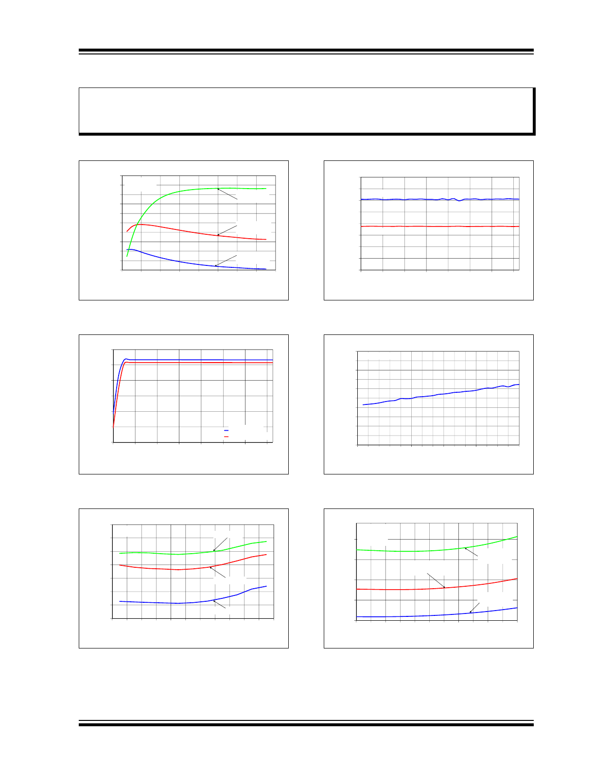
FIGURE 2-7:
EA Output Current vs.
Temperature.
FIGURE 2-8:
EA Transconductance vs.
Temperature.
FIGURE 2-9:
Efficiency vs. Output
Current (V
IN
= 12V).
FIGURE 2-10:
Efficiency vs. Output
Current (V
IN
= 5V).
FIGURE 2-11:
Output Voltage vs. Output
Current (V
OUT
= 0.9V).
FIGURE 2-12:
Output Voltage vs. Output
Current (V
OUT
= 1.0V).
-800
-600
-400
-200
0
200
400
600
800
-40
-20
0
20
40
60
80
100
120
140
EA
Output
Current (µA)
Temperature(°C)
V
IN
= 12V
Sinking
Sourcing
0.6
0.8
1
1.2
1.4
1.6
1.8
2
-40
-20
0
20
40
60
80
100
120
140
EA
T
ransconductance
(m
S)
Temperature (°C)
V
IN
= 12V
V
OUT
= 1.0V
0.00%
10.00%
20.00%
30.00%
40.00%
50.00%
60.00%
70.00%
80.00%
90.00%
100.00%
0
0.5
1
1.5
2
2.5
3
3.5
4
4.5
5
Efficienc
y
(%
)
I
OUT
(A)
12
12
12
12
12
12
12
12
12
0.7V
0.8V
0.9V
1.0V
1.2V
1.5V
1.8V
2.5V
3.3V
0.00%
10.00%
20.00%
30.00%
40.00%
50.00%
60.00%
70.00%
80.00%
90.00%
100.00%
0
0.5
1
1.5
2
2.5
3
3.5
4
4.5
5
E
ffic
iency
(%
)
I
OUT
(A)
5
5
5
5
5
5
5
5
5
0.7V
0.8V
0.9V
1.0V
1.2V
1.5V
1.8V
2.5V
3.3V
0.891
0.893
0.895
0.897
0.899
0.901
0.903
0.905
0.907
0.909
0
0.5
1
1.5
2
2.5
3
3.5
4
4.5
5
V
OUT
(V
)
I
OUT
(A)
5
12
V
IN
= 12V
V
IN
= 5V
0.990
0.995
1.000
1.005
1.010
0
0.5
1
1.5
2
2.5
3
3.5
4
4.5
5
V
OUT
(V
)
I
OUT
(A)
5
12
V
IN
= 12V
V
IN
= 5V
2015 Microchip Technology Inc.
DS20005478A-page 9
MIC45404
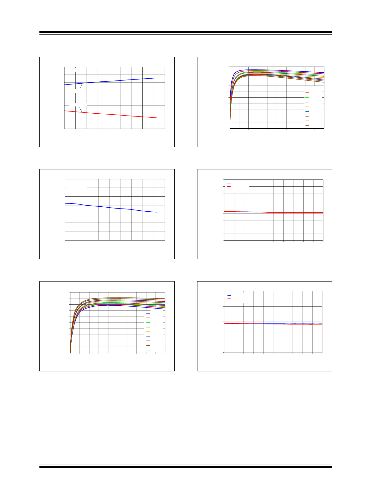
Note:
Unless otherwise indicated, V
IN
= 12V; C
VDDA
= 2.2 µF, T
A
= +25°C.
FIGURE 2-13:
Output Voltage vs. Output
Current (V
OUT
= 1.2V).
FIGURE 2-14:
Output Voltage vs. Output
Current (V
OUT
= 1.5V).
FIGURE 2-15:
Output Voltage vs. Output
Current (V
OUT
= 1.8V).
FIGURE 2-16:
Output Voltage vs. Output
Current (V
OUT
= 2.5V).
FIGURE 2-17:
Output Voltage vs. Output
Current (V
OUT
= 3.3V).
1.190
1.192
1.194
1.196
1.198
1.200
1.202
1.204
1.206
1.208
1.210
0
0.5
1
1.5
2
2.5
3
3.5
4
4.5
5
V
OUT
(V)
I
OUT
(A)
5
12
V
IN
= 12V
V
IN
= 5V
1.490
1.495
1.500
1.505
1.510
0
0.5
1
1.5
2
2.5
3
3.5
4
4.5
5
V
OUT
(V
)
I
OUT
(A)
5
12
V
IN
= 12V
V
IN
= 5V
1.790
1.795
1.800
1.805
1.810
0
0.5
1
1.5
2
2.5
3
3.5
4
4.5
5
V
OUT
(V)
I
OUT
(A)
5
12
V
IN
= 12V
V
IN
= 5V
2.480
2.485
2.490
2.495
2.500
0
0.5
1
1.5
2
2.5
3
3.5
4
4.5
5
V
OUT
(V)
I
OUT
t (A)
5
12
V
IN
= 12V
V
IN
= 5V
3.290
3.292
3.294
3.296
3.298
3.300
3.302
3.304
3.306
3.308
3.310
0
0.5
1
1.5
2
2.5
3
3.5
4
4.5
5
V
OU
T
(V)
I
OUT
(A)
5
12
V
IN
= 12V
V
IN
= 5V
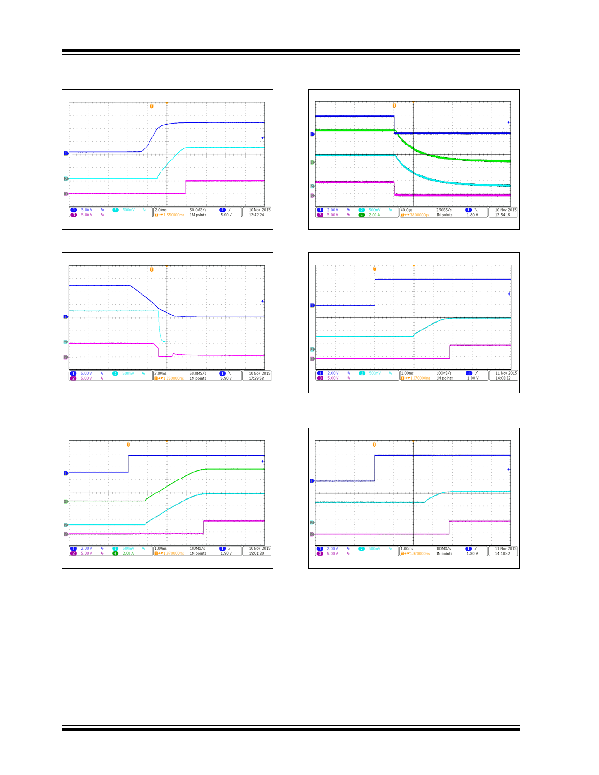
MIC45404
DS20005478A-page 10
2015 Microchip Technology Inc.
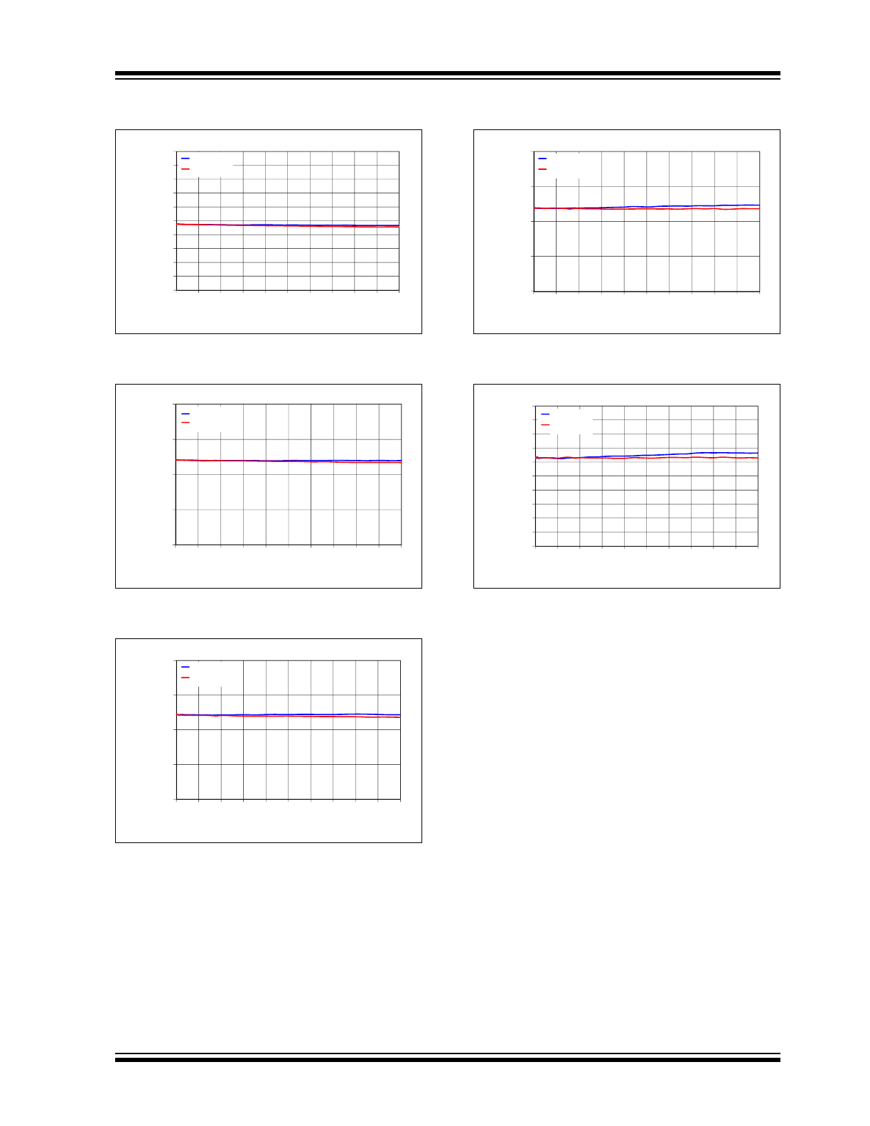
Note:
Unless otherwise indicated, V
IN
= 12V; C
VDDA
= 2.2 µF, T
A
= +25°C.
FIGURE 2-18:
V
IN
Turn-On.
FIGURE 2-19:
V
IN
Turn-Off.
FIGURE 2-20:
Enable Turn-On.
FIGURE 2-21:
Enable Turn-Off.
FIGURE 2-22:
Enable Start-up w/Pre-Biased
Output.
FIGURE 2-23:
Enable Start-up
w/Pre-Biased Output.
V
IN
= 12V
V
OUT =
1.2V
R
LOAD
= 0.3
f
SW
= 400 kHz
V
IN
(5V/div)
V
OUT
(500 mV/div)
PG
(5V/div)
Time (2 ms/div)
V
IN
(5V/div)
V
OUT
(500 mV/div
PG
(5V/div)
V
IN
= 12V
V
OUT =
1.2V
R
LOAD
= 0.6
f
SW
= 400 kHz
Time (2 ms/div)
EN/DLY
(2V/div
V
OUT
(500 mV/div)
PG
(5V/div)
V
IN
= 12V
V
OUT =
1.2V
R
OUT
= 0.24
f
SW
= 400 kHz
I
OUT
(2A/div)
Time (1 ms/div)
EN/DLY
(2V/div
V
OUT
(500 mV/div)
PG
(5V/div)
V
IN
= 12V
V
OUT =
1.2V
R
OUT
= 0.24
f
SW
= 400 kHz
I
OUT
(2A/div)
Time (40 µs/div)
EN/DLY
(2V/div
V
OUT
(500 mV/div)
PG
(5V/div)
V
IN
= 12V
V
OUT =
1.2V
V
PRE-BIAS
= 0.6V
f
SW
= 400 kHz
Time (1 ms/div)
EN/DLY
(2V/div
V
OUT
(500 mV/div)
PG
(5V/div)
V
IN
= 12V
V
OUT =
1.2V
V
PRE-BIAS
= 1.0V
f
SW
= 400 kHz
Time (1 ms/div)