
2017 Microchip Technology Inc.
DS20005873A-page 1
MIC2877
Features
• Typical 6.5A Input Peak Current Limit
• Up to 95% Efficiency
• Fully Integrated, High-Efficiency, 2 MHz Switching
Frequency
• Bidirectional True Load Disconnect, Overvoltage
Protection (OVP) and Undervoltage Lockout
(UVLO)
• Controlled Pre-Charge Current Limit at Start-Up
• Ultra-Fast Transient Response
• Input Voltage Range from 2.5V to 5.5V
• Maximum Output Current:
- 1.5A, V
IN
= 2.5V and V
OUT
= 5V
- 2A,V
IN
= 3V and V
OUT
= 5V
• Output Voltage Range:
- Adjustable
- Fixed Versions: 4.75V, 5V, 5.25V, 5.5V
• Integrated Anti-Ringing Switch for
Electromagnetic Interference (EMI) Reduction
• Typically Less than 2 µA Shutdown Current
• Internal Compensation
• Bypass Mode for V
IN
≥ V
OUT
• Power Good (PG) Output
• Overcurrent Protection and Thermal Shutdown
• Fixed and Adjustable Output Versions
• Available Package: 8-pin FTQFN 2 x 2 mm
Applications
• USB OTG and HDMI Hosts
• Portable Power Reserve Supplies
• High-Current Parallel Lithium Cell Applications
• Portable Equipment
General Description
The MIC2877 is a compact and highly efficient 2 MHz
synchronous boost regulator with a typically 6.5A
switch. It features a bidirectional true load disconnect
function that prevents any leakage current between the
input and output when the device is disabled
(EN = GND), it protects the input supply and improves
the start-up performance.
The MIC2877 has the input voltage range between
2.5V and 5.5V and provides a 2A output continuous
current for V
IN
= 3.0V and V
OUT
= 5V. Fixed and
adjustable versions are available.
The MIC2877 operates in Bypass mode automatically
when the input voltage is higher or equal to the target
output voltage. At light loads, the boost converter goes
to Pulse Frequency Modulation (PFM) mode to
improve the efficiency. In Shutdown mode (EN = GND),
the regulator typically consumes less than 2 µA.
The MIC2877 also features an integrated anti-ringing
switch to minimize EMI, overvoltage and overcurrent
protection, UVLO and thermal shutdown.
The MIC2877 is available in an 8-pin FTQFN 2 x 2 mm
package.
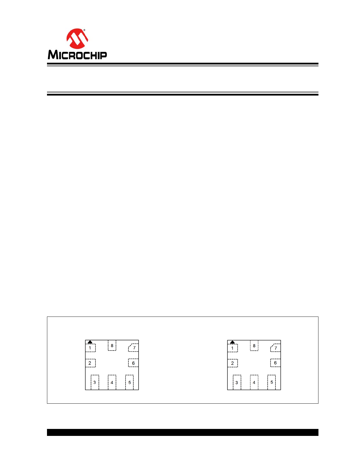
Package Types
MIC2877
(Fixed Output)
8-pin 2 x 2 mm FTQFN
MIC2877
(Adjustable Output)
8-pin 2 x 2 mm FTQFN
A
GND
V
IN
P
GND
V
OUT
SW
PG
EN
V
OUTS
A
GND
V
IN
P
GND
V
OUT
SW
PG
EN
FB
2 MHz Synchronous Low Voltage Step-Up Regulator
with 6.5A Switch and Bidirectional Load Disconnect
MIC2877
DS20005873A-page 2
2017 Microchip Technology Inc.
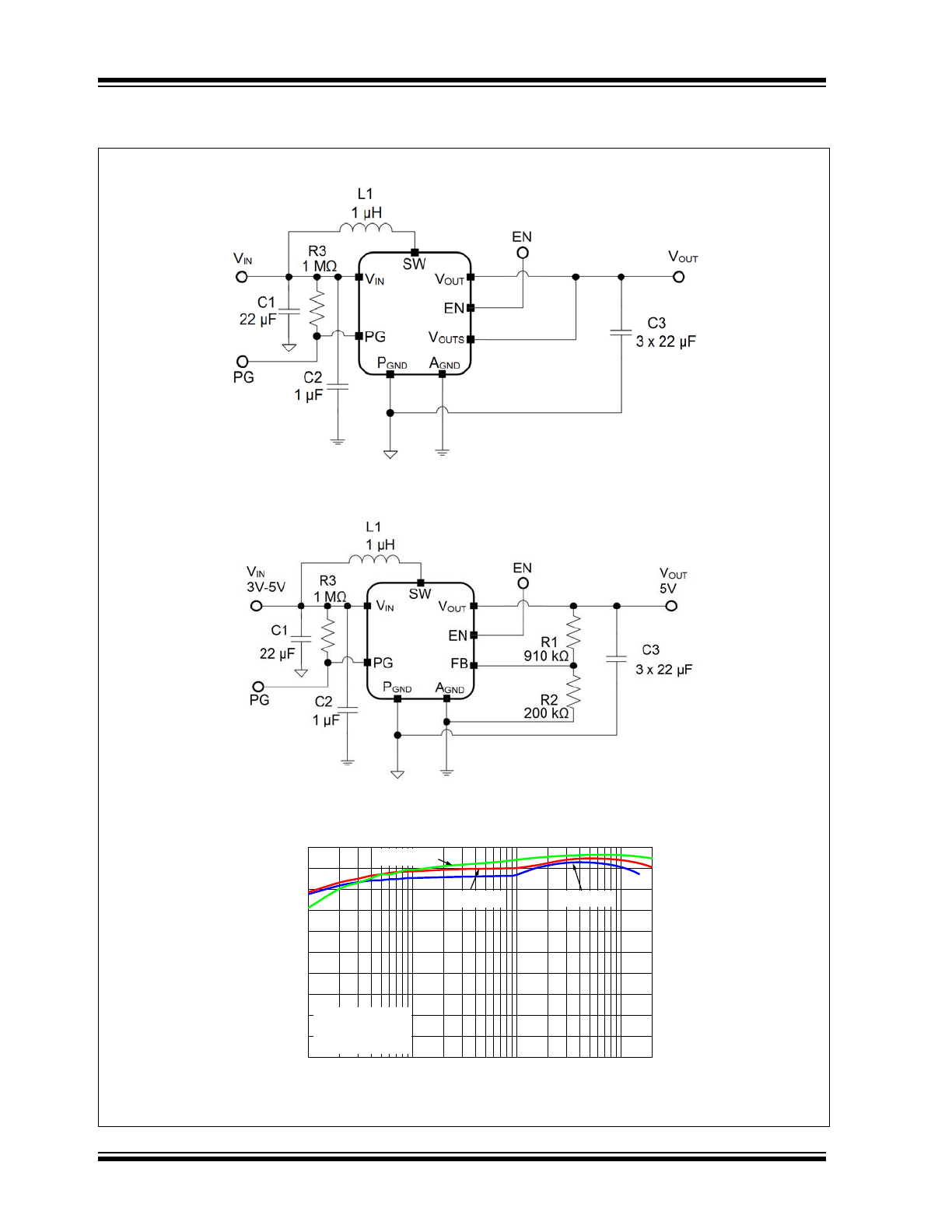
Typical Application Schematics
MIC2877 (Fixed Output)
MIC2877 (Adjustable Output)
MIC2877 Efficiency vs. Load Current
0
10
20
30
40
50
60
70
80
90
100
1
10
100
1000
Efficiency
(%
)
I
OUT
(mA)
V
OUT
= 5V
L = 1 µH
C
OUT
= 3 x 22 µF
V
IN
= 2.5V
V
IN
= 3.3V
V
IN
= 4.5V
2017 Microchip Technology Inc.
DS20005873A-page 3
MIC2877
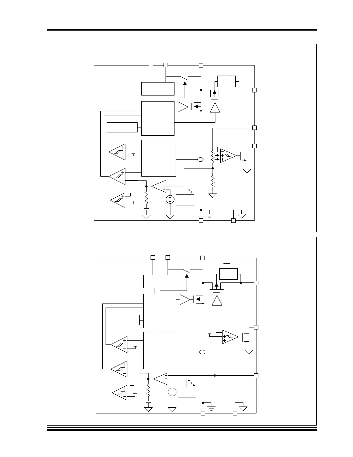
Functional Block Diagrams
MIC2877 (Fixed Output)
OUT
/PG
OUTS
REFERENCE
GENERATOR
EN
V
IN
PWM
LOGIC
CONTROL
+
MINIMUM
SWITCHING
2 MHz
OSCILLATOR
CURRENT
SENSE
+
SLOPE
COMPENSATION
PWM
VREF
SOFT
START
V
IN
BODY
DRIVER
OC
OV FB
OV REF
SW
HS
DRIVER
LS
DRIVER
A
GND
OVP
P
GND
ANTI -
RINGING
V
IN
6A
MIC2877 (Adjustable Output)
REFERENCE
GENERATOR
EN
V
IN
PWM
LOGIC
CONTROL
+
MINIMUM
SWITCHING
2 MHz
OSCILLATOR
CURRENT
SENSE
+
SLOPE
COMPENSATION
PWM
VREF
SOFT
START
V
IN
BODY
DRIVER
OC
PGL
PGH
OV FB
OV REF
SW
OUT
/PG
FB
HS
DRIVER
LS
DRIVER
A
GND
OVP
P
GND
ANTI -
RINGING
6.5A

MIC2877
DS20005873A-page 4
2017 Microchip Technology Inc.
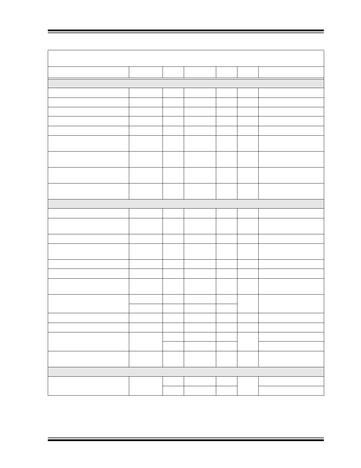
1.0
ELECTRICAL CHARACTERISTICS
Absolute Maximum Ratings †
V
IN
, EN, OUT, FB/V
OUTs
, PG, SW to P
GND
.................................................................................................. –0.3V to +6V
A
GND
to P
GND
............................................................................................................................................ –0.3V to +0.3V
EN to A
GND
.................................................................................................................................................. –0.3V to +6V
Power Dissipation............................................................................................................................... Internally Limited
(
1
)
Lead Temperature (soldering, 10 seconds)...........................................................................................................+260°C
Junction Temperature (T
J
)......................................................................................................................–40°C to +150°C
Storage Temperature (T
S
) ......................................................................................................................–40°C to +150°C
ESD Rating Human Body Model (HBM)
(
2
)
.................................................................................................................2 kV
ESD Rating Machine Model (MM)
(
2
)
.........................................................................................................................200V
Operating Ratings ‡
Supply Voltage (V
IN
).................................................................................................................................. +2.5V to +5.5V
Output Voltage (V
OUT
)................................................................................................................................... V
IN
to +5.5V
Enable Voltage (V
EN
) ......................................................................................................................................... 0V to V
IN
Junction Temperature (T
J
)......................................................................................................................–40°C to +125°C
Operating Ambient Temperature (T
A
).......................................................................................................–40°C to +85°C
Package Thermal Resistance FTQFN22-8LD (
JA
) ........................................................................................... +50°C/W
†
Notice: Stresses above those listed under “Absolute Maximum Ratings” may cause permanent damage to the device.
This is a stress rating only and functional operation of the device at those or any other conditions above those indicated
in the operational sections of this specification is not intended. Exposure to maximum rating conditions for extended
periods may affect device reliability.
‡ Notice:
The device is not guaranteed to function outside its operating ratings.
Note 1:
The maximum allowable power dissipation of any T
A
(ambient temperature) is P
D(max)
= (T
J(max)
– T
A
)/θ
JA
.
Exceeding the maximum allowable power dissipation will result in excessive die temperature, and the
regulator will go into thermal shutdown.
2:
Devices are ESD sensitive. Handling precautions are recommended. Human body model, 1.5 kΩ in series
with 100 pF.
2017 Microchip Technology Inc.
DS20005873A-page 5
MIC2877
ELECTRICAL CHARACTERISTICS
Electrical Characteristics:
V
IN
= 3V, V
OUT
= 5V, C
IN
= 22 µF, C
OUT
= 3 x 22 µF, L = 1 µH, T
A
= +25°C. Bold values
are valid for –40°C ≤ T
A
< +85°C, unless otherwise noted. (
Note 1
)
Parameters
Sym.
Min.
Typ.
Max.
Units
Conditions
Power Supply
Supply Voltage Range
V
IN
2.5
—
5.5
V
Output Voltage
V
OUT
V
IN
—
5.5
V
UVLO Rising Threshold
UVLO
(r)
—
2.29
2.49
V
UVLO Hysteresis
UVLO
HYS
—
200
—
mV
Quiescent Current
I
VIN
—
125
180
µA
Non-Switching
V
IN
Shutdown Current
I
VINSD
—
1
3
µA
V
IN
= 5.5V, V
OUT
= 0V,
EN = 0
V
OUT
Shutdown Current
I
VOUTSD
—
1
3
µA
V
IN
= 0V, V
OUT
= 5.5V,
EN = 0
Overtemperature Shutdown
Threshold
T
SD
—
+155
—
°C
Overtemperature Shutdown
Hysteresis
T
SD-HYS
—
+15
—
°C
Boost Converter
Feedback Voltage
V
FB
0.8865
—
0.9135
V
Adjustable version
Line Regulation
—
—
0.3
—
%
2.5V < V
IN
< 4.5V,
I
OUT
= 0.5A
Load Regulation
—
—
0.2
—
%/A
I
OUT
= 300 mA to 1.2A
Overvoltage Protection
Threshold
V
OVD
6.6
—
6.75
V
Minimum Controllable On Time
T
ONMIN
—
35
—
ns
Maximum Duty Cycle
D
MAX
—
93.6
—
%
Low-Side Switch Current Limit
(
Note 2
)
I
SW
4.8
6.5
7.2
A
V
IN
= 3V, V
OUT
= 5V
Switch-on Resistance
R
PMOS
—
45
—
mΩ
V
IN
= 3V, V
OUT
= 5V,
I
SW
= 200 mA
R
NMOS
—
33
—
Switch Leakage Current
I
SW
—
0.2
5
µA
V
EN
= 0V, V
SW
= 5.5V
Oscillator Frequency
f
SW
1.6
2
2.4
MHz
Pre-Charge Current Limit
I
PRE-CHARGE
0.27
0.5
0.76
A
V
OUT
0.5V
1.7
2.55
3.2
V
IN
= 4.5V, V
OUT
= 3V
Soft Start Charge Time
I
SS
—
1.1
2
ms
V
OUT
= 5V, V
IN
= 3V,
C
OUT
= 22 µF x 3
EN/PG Control Pins
EN Threshold (
Note 3
)
V
EN
1.5
—
V
IN
V
Device enabled
—
—
0.4
Device disabled
Note 1:
Specification for packaged product only.
2:
Data from design and characterization. Not production tested.
3:
If the EN pin is externally driven High before V
IN
is applied, a 200kΩ series resistor is required on the EN
signal to the pin.
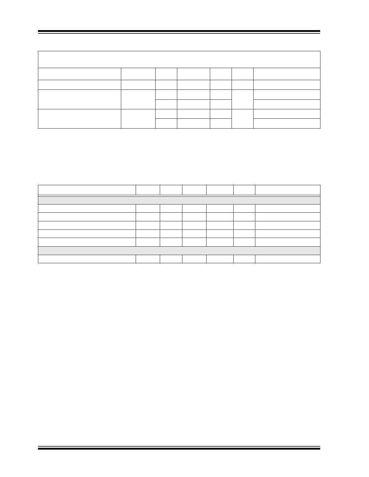
MIC2877
DS20005873A-page 6
2017 Microchip Technology Inc.
EN Input Current
—
—
1.5
—
µA
EN = 3V
Power Good Threshold (Rising)
V
PG-THR
—
0.91 x V
FB
—
V
Adjustable version
—
0.91 x V
OUT
—
Fixed version
Power Good Threshold (Falling)
V
PG-THF
—
0.82 x V
FB
—
V
Adjustable version
—
0.83 x V
OUT
—
Fixed version
ELECTRICAL CHARACTERISTICS (CONTINUED)
Electrical Characteristics:
V
IN
= 3V, V
OUT
= 5V, C
IN
= 22 µF, C
OUT
= 3 x 22 µF, L = 1 µH, T
A
= +25°C. Bold values
are valid for –40°C ≤ T
A
< +85°C, unless otherwise noted. (
Note 1
)
Parameters
Sym.
Min.
Typ.
Max.
Units
Conditions
Note 1:
Specification for packaged product only.
2:
Data from design and characterization. Not production tested.
3:
If the EN pin is externally driven High before V
IN
is applied, a 200kΩ series resistor is required on the EN
signal to the pin.
TEMPERATURE SPECIFICATIONS
Parameters
Sym.
Min.
Typ.
Max.
Units
Conditions
Temperature Ranges
Power Dissipation
—
—
—
—
—
Internally Limited
(
1
)
Lead Temperature
—
—
—
+260
°C
Soldering, 10s
Junction Temperature
T
J
–40
—
+125
°C
Storage Temperature
T
S
–40
—
+150
°C
Operating Ambient Temperature
T
A
–40
—
+85
°C
Package Thermal Resistances
Thermal Resistance FTQFN22-8LD
JA
—
+50
—
°C/W
Note 1:
The maximum allowable power dissipation of any T
A
(ambient temperature) is
P
D(max)
= (T
J(max)
– T
A
)/θ
JA
. Exceeding the maximum allowable power dissipation will result in excessive
die temperature, and the regulator will go into thermal shutdown.
2017 Microchip Technology Inc.
DS20005873A-page 7
MIC2877
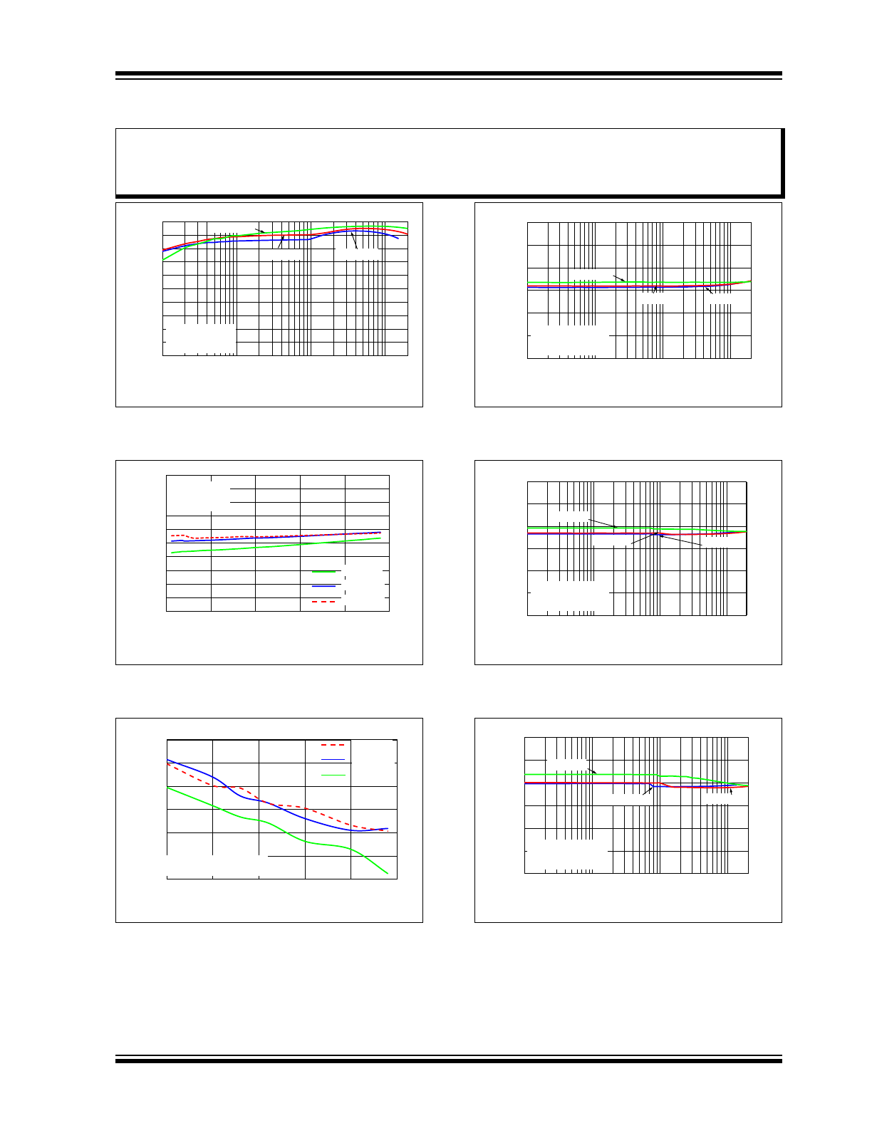
2.0
TYPICAL PERFORMANCE CURVES
FIGURE 2-1:
Efficiency vs. Load Current,
Adjustable Output Version.
FIGURE 2-2:
Output Voltage vs. Load
Current, Adjustable Output Version.
FIGURE 2-3:
Switching Frequency vs.
Input Voltage, Adjustable Output Version.
FIGURE 2-4:
Feedback Voltage vs. Load
Current (T
A
=
–
40°C), Adjustable Output Version.
FIGURE 2-5:
Feedback Voltage vs. Load
Current (T
A
=
+
25°C), Adjustable Output Version.
FIGURE 2-6:
Feedback Voltage vs. Load
Current (T
A
= +85°C), Adjustable Output Version.
Note:
The graphs and tables provided following this note are a statistical summary based on a limited number of
samples and are provided for informational purposes only. The performance characteristics listed herein
are not tested or guaranteed. In some graphs or tables, the data presented may be outside the specified
operating range (e.g., outside specified power supply range) and therefore outside the warranted range.
0
10
20
30
40
50
60
70
80
90
100
1
10
100
1000
Efficiency
(%
)
I
OUT
(mA)
V
OUT
= 5V
L = 1 µH
C
OUT
= 3 x 22 µF
V
IN
= 2.5V
V
IN
= 3.3V
V
IN
= 4.5V
4.9
4.92
4.94
4.96
4.98
5
5.02
5.04
5.06
5.08
5.1
0
0.25
0.5
0.75
1
1.25
V
OUT
(V)
I
OUT
(A)
V
IN
= 3V
L = 1 µH
C
OUT
= 3 x 22 µF
T
A
= +25°C
T
A
= +85°C
T
A
= -40°C
1900
1920
1940
1960
1980
2000
2020
2.5
3
3.5
4
4.5
5
Sw
itching Frequency
(kHz)
Input Voltage (V)
V
OUT
= 5V, I
OUT
= 0.5A
L = 1 µH, C
OUT
= 3 x 22 µF
T
A
= +25°C
T
A
= +85°C
T
A
= -40°C
0.87
0.88
0.89
0.9
0.91
0.92
0.93
1
10
100
1000
Feedback V
oltage (V)
I
OUT
(mA)
V
OUT
= 5V
L = 1 µH, T
A
= -40
o
C
C
OUT
= 3 x 22 µF
V
IN
= 2.5V
V
IN
= 3.3V
V
IN
= 4.5V
0.87
0.88
0.89
0.9
0.91
0.92
0.93
1
10
100
1000
Feedback V
oltage (V)
I
OUT
(mA)
V
OUT
= 5V
L = 1 µH, T
A
= +25
o
C
C
OUT
= 3 x 22 µF
V
IN
= 2.5V
V
IN
= 3.3V
V
IN
= 4.5V
0.87
0.88
0.89
0.9
0.91
0.92
0.93
1
10
100
1000
Feedback V
oltage (V)
I
OUT
(mA)
V
OUT
= 5V
L = 1 µH, T
A
= +85
o
C
C
OUT
= 3 x 22 µF
V
IN
= 2.5V
V
IN
= 3.3V
V
IN
= 4.5V
MIC2877
DS20005873A-page 8
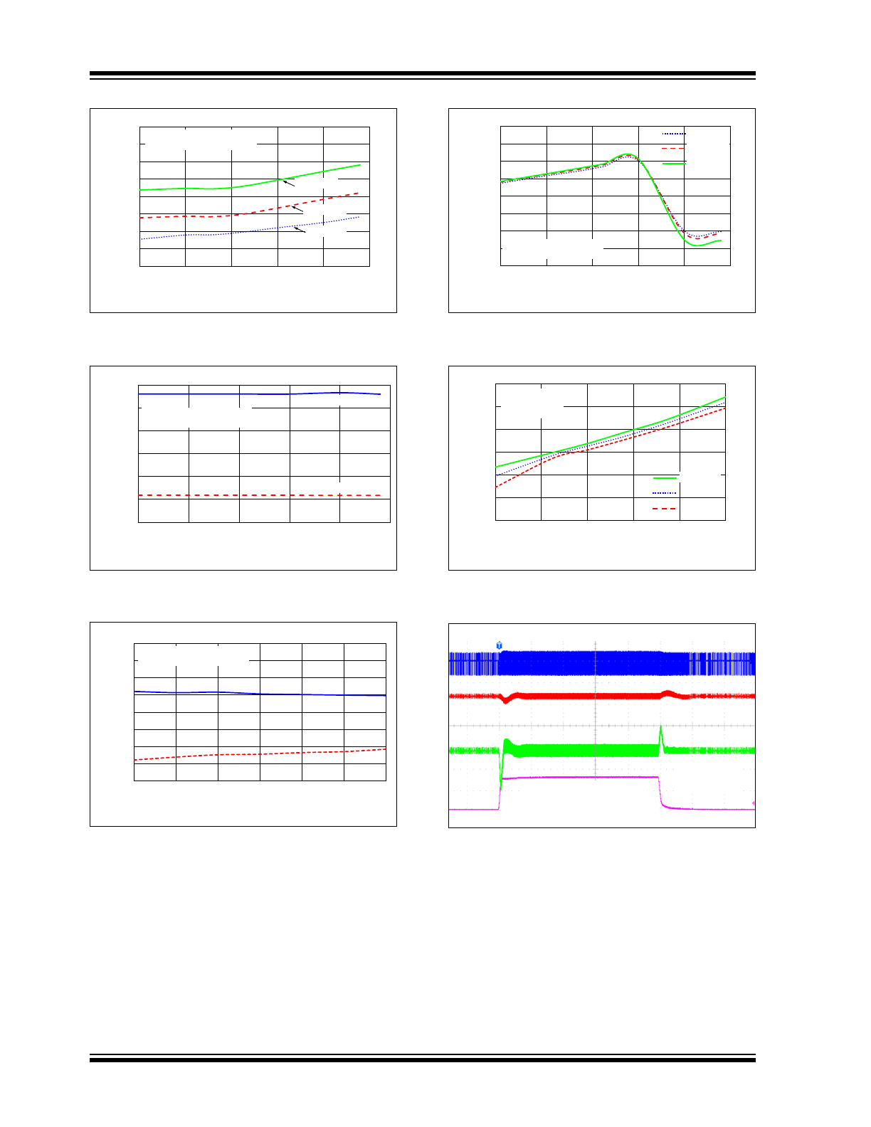
2017 Microchip Technology Inc.
FIGURE 2-7:
Shutdown Current vs. Input
Voltage, Adjustable Output Version.
FIGURE 2-8:
Power Good Threshold vs.
Input Voltage, Adjustable Output Version.
FIGURE 2-9:
UVLO Threshold vs. Load
Current, Adjustable Output Version.
FIGURE 2-10:
Enable to Start-Up Delay vs.
Input Voltage, Adjustable Output Version.
FIGURE 2-11:
Maximum Output Current
vs. Input Voltage, Adjustable Output Version.
FIGURE 2-12:
Load Transient (V
IN
= 3.3V),
Adjustable Output Version
.
0
0.25
0.5
0.75
1
1.25
1.5
1.75
2
2.5
3
3.5
4
4.5
5
Shutdow
n
Current
(µA)
Input Voltage (V)
V
OUT
= 5V, EN = GND
Shutdown Mode, No Load
T
A
= -40
o
C
T
A
= +25
o
C
T
A
= +85
o
C
0.8
0.82
0.84
0.86
0.88
0.9
0.92
2.5
3
3.5
4
4.5
5
PG Threshold/V
FB
Input Voltage (V)
V
OUT
= 5V, I
OUT
= 0A
L = 1 µH, C
OUT
= 3 x 22 µF
RISING
FALLING
2.1
2.15
2.2
2.25
2.3
2.35
2.4
2.5
0
0.05
0.1
0.15
0.2
0.25
0.3
UVLO
Threshold
(V
Load Current (A)
V
OUT
= 5V, T
A
= +25
o
C
L = 1 µH, C
OUT
= 3 x 22 µF
RISING
FALLING
0
0.2
0.4
0.6
0.8
1
1.2
1.4
1.6
2.5
3
3.5
4
4.5
5
EN to Start-
Up Delay
(ms)
Input Voltage (V)
V
OUT
= 5V, I
OUT
= 1A
L = 1 µH, C
OUT
= 3 x 22 µF
T
A
= +25°C
T
A
= +85°C
T
A
= -40°C
0
1000
3000
4000
5000
6000
2.5
2.9
3.3
3.7
4.1
4.5
I
OU
7
Max
(mA)
V
IN
(V)
V
OUT
= 5V
L = 1 µH
C
OUT
= 3 x 22 µF
T
A
= +25°C
T
A
= +85°C
T
A
= -40°C
V
IN
= 3.3V
V
OUT
= 5V
Load Step: 0.01A to 1.5A
T
A
= 25°C
V
SW
5V/div
PG
2V/div
V
OUT
200 mV/div
AC Coupled
I
OUT
1A/div
400 µs/div
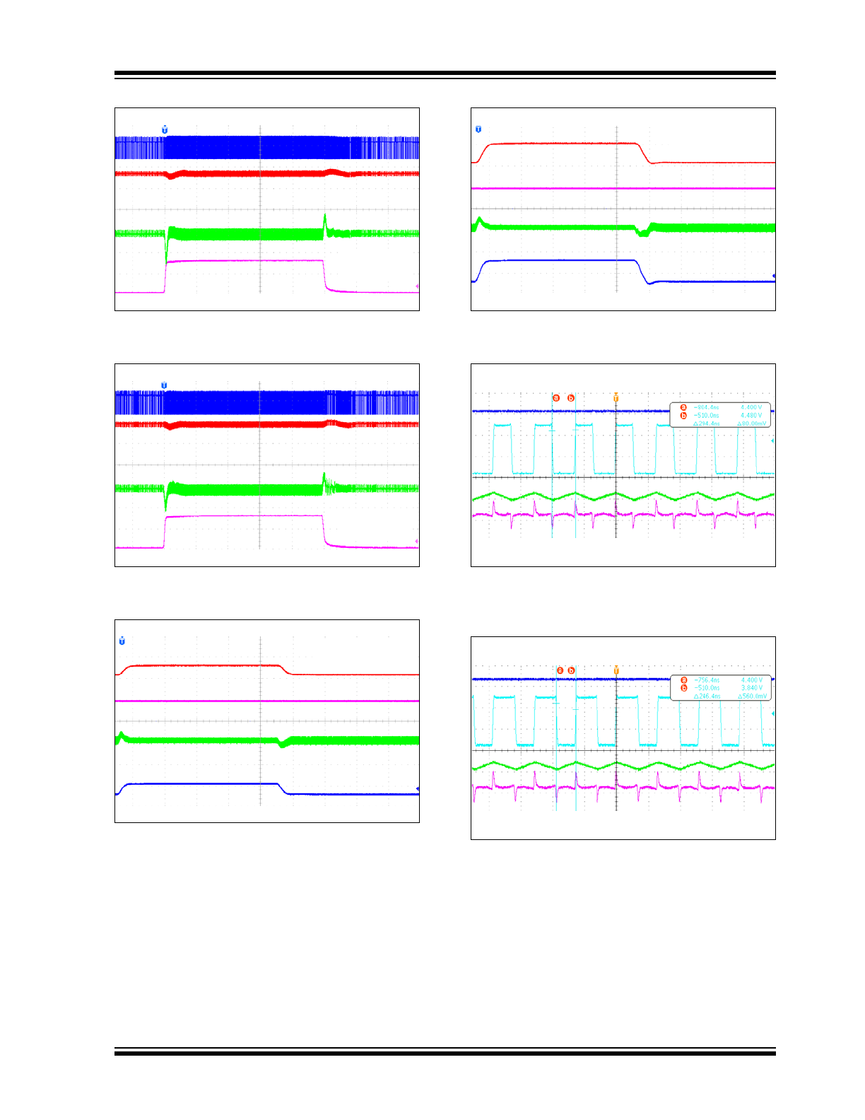
2017 Microchip Technology Inc.
DS20005873A-page 9
MIC2877
FIGURE 2-13:
Load Transient
(
V
IN
= 4V),
Adjustable Output Version
.
FIGURE 2-14:
Load Transient
(
V
IN
= 4.75V), Adjustable Output Version.
FIGURE 2-15:
Line Transient (V
IN
=
2.5V to
3.5V),
Adjustable Output Version
.
FIGURE 2-16:
Line Transient (V
IN
=
2.5V to
4.5V),
Adjustable Output Version
.
FIGURE 2-17:
Switching Waveforms
(V
IN
= 2.5V, V
OUT
= 5V, I
OUT
=
1.5A),
Adjustable
Output Version
.
FIGURE 2-18:
Switching Waveforms
(V
IN
= 3V, V
OUT
= 5V, I
OUT
=
2A),
Adjustable
Output Version.
V
IN
= 4V
V
OUT
= 5V
Load Step: 0.01A to 1.5A
T
A
= 25°C
V
SW
5V/div
PG
2V/div
V
OUT
200 mV/div
AC Coupled
I
OUT
1A/div
400 µs/div
V
IN
=4.75V
V
OUT
= 5V
Load Step: 0.01A to 1.5A
T
A
= 25°C
V
SW
5V/div
PG
2V/div
V
OUT
200 mV/div
AC Coupled
I
OUT
1A/div
400 µs/div
V
IN
= 2.5V to 3.5V
I
OUT
= 1A
V
OUT
= 5V
L = 1 µH
C
OUT
= 3 x 22 µF
PG
2V/div
I
OUT
1A/div
V
OUT
200 mV/div
AC Coupled
V
IN
2V/div
400 µs/div
V
IN
= 2.5V to 4.5V
I
OUT
= 1A
V
OUT
= 5V
L = 1 µH
C
OUT
= 3 x 22 µF
PG
2V/div
I
OUT
1A/div
V
OUT
200 mV/div
AC Coupled
V
IN
2V/div
400 µs/div
PG
2V/div
V
SW
2V/div
V
OUT
50 mV/div, AC Coupled
I
L
2A/div
400 ns/div
PG
2V/div
V
SW
2V/div
V
OUT
50 mV/div, AC Coupled
I
L
2A/div
400 ns/div
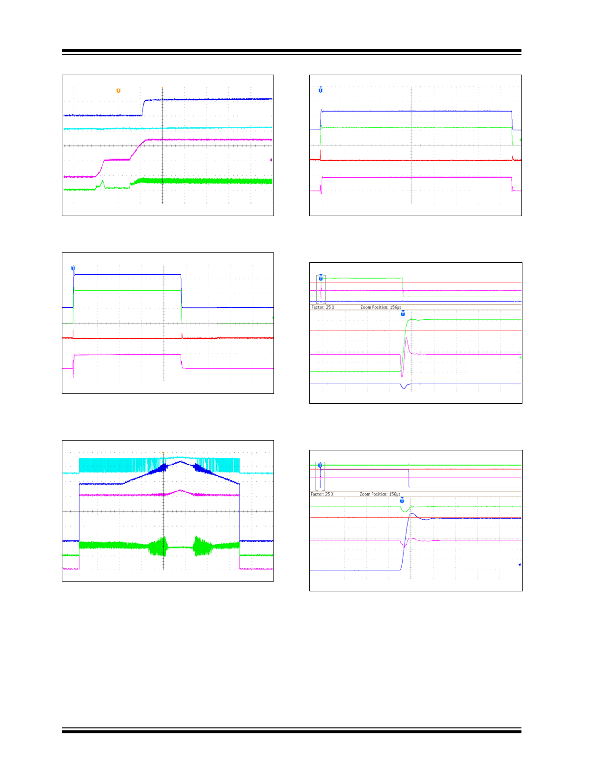
MIC2877
DS20005873A-page 10
2017 Microchip Technology Inc.
FIGURE 2-19:
Soft Start in Boost Mode,
Adjustable Output Version.
FIGURE 2-20:
Start-Up in Short Circuit
(V
IN
= 4.5V, T
A
= +25°C), Adjustable Output
Version.
FIGURE 2-21:
Bypass Mode, Adjustable
Output Version.
FIGURE 2-22:
Start-Up in Short Circuit
(V
IN
= 2.5V, T
A
= +25°C), Adjustable Output
Version.
FIGURE 2-23:
Bidirectional True
Shutdown. Shorted Input, Output Step from 0V to
5V with EN = 0V. Adjustable Output Version.
FIGURE 2-24:
Bidirectional True
Shutdown. Shorted Output, Supply Step from 0V
to 5.0V with EN = 0V. Adjustable Output Version.
VIN = 3.3V
VOUT = 5V
IOUT = 0.5A
Resistive Load
PG
2V/div
EN
2V/div
V
OUT
2V/div
I
L
2A/div
400 µs/div
V
SW
2v/div
EN
2V/div
PG
500 mV/div
I
OUT
500 mA/div
V
OUT
= 5V
V
IN
= 4.5V
L = 1 µH
C
OUT
= 3 x 22 µF
4 ms/div
V
SW
5V/div
V
IN
1V/div
V
OUT
1V/div
I
L
1A/div
V
IN
= 4V to 5.5V
V
OUT
= 5V
I
OUT
= 0.5A
1s/div
V
SW
2V/div
EN
2V/div
PG
500 mV/div
I
OUT
500 mA/div
V
OUT
= 5V
V
IN
= 2.5V
L = 1 µH
C
OUT
= 3 x 22 µF
4 ms/div
PG
5V/div
I
IN
500 mA/div
V
OUT
1V/div
V
IN
1V/div
V
IN
= GND = EN
V
OUT
= 0 to 5V step
C
IN
= 22 µF, L = 1 µH
C
OUT
= 3 x 22 µF
400 µs/div
V
OUT
1V/div
PG
5V/div
I
OUT
500 mA/div
V
IN
1V/div
V
OUT
= GND = EN
V
IN
= 0 to 5V step
C
IN
= 22 µF, L = 1 µH
C
OUT
= 3 x 22 µF
400 µs/div