
2015 Microchip Technology Inc.
DS20005549A-page 1
MIC2875
Features
• Up to 95% Efficiency
• Input Voltage Range: 2.5V to 5.5V
• Fully-Integrated, High-Efficiency, 2 MHz
Synchronous Boost Regulator
• Bi-Directional True Load Disconnect
• Integrated Anti-Ringing Switch
• Minimum Switching Frequency of 45 kHz
• <1 μA Shutdown Current
• Bypass Mode for V
IN
≥ V
OUT
• Overcurrent Protection and Thermal Shutdown
• Fixed and Adjustable Output Versions
• 8-pin 2 mm × 2 mm TDFN Package
Applications
• Tablet and Smartphones
• USB OTG and HDMI Hosts
• Portable Power Reserve Supplies
• Low-Noise Audio Applications
• Portable Equipment
General Description
The MIC2875 is a compact and highly-efficient 2 MHz
synchronous boost regulator with a 4.8A switch. It
features a bi-directional load disconnect function which
prevents any leakage current between the input and
output when the device is disabled. The MIC2875
operates in bypass mode automatically when the input
voltage is greater than the target output voltage. At light
loads, the boost converter goes to the PFM mode to
improve the efficiency.
To minimize switching artifacts in the audio band, the
MIC2875 is designed to operate with a minimum
switching frequency of 45 kHz. The MIC2875 also
features an integrated anti-ringing switch to minimize
EMI.
The MIC2875 is available in a 8-pin 2 mm × 2 mm Thin
DFN (TDFN) package, with a junction temperature
range of –40°C to +125°C.
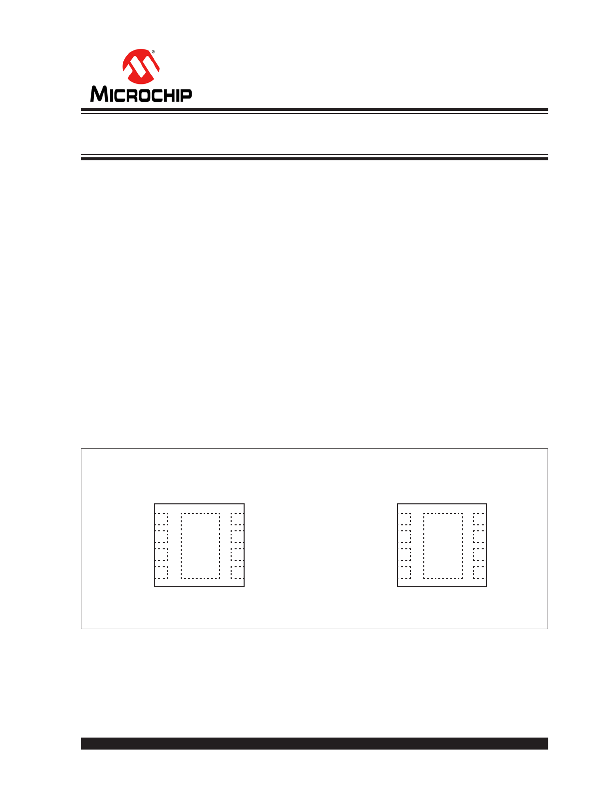
Package Type
MIC2875 (F
IXED
O
UTPUT
)
8-Pin 2x2 TDFN* (MT)
(Top View)
MIC2875 (A
DJ
. O
UTPUT
)
8-Pin 2x2 TDFN* (MT)
(Top View)
SW
PGND
IN
AGND
OUT
/PG
EN
FB
▲
EP
1
2
3
4
5
6
7
8
SW
PGND
IN
AGND
OUT
/PG
EN
OUTS
▲
EP
1
2
3
4
5
6
7
8
* Includes exposed thermal pad (EP), see
Table 3-1
.
4.8A I
SW
, Synchronous Boost Regulator
with Bi-Directional Load Disconnect
MIC2875
DS20005549A-page 2
2015 Microchip Technology Inc.
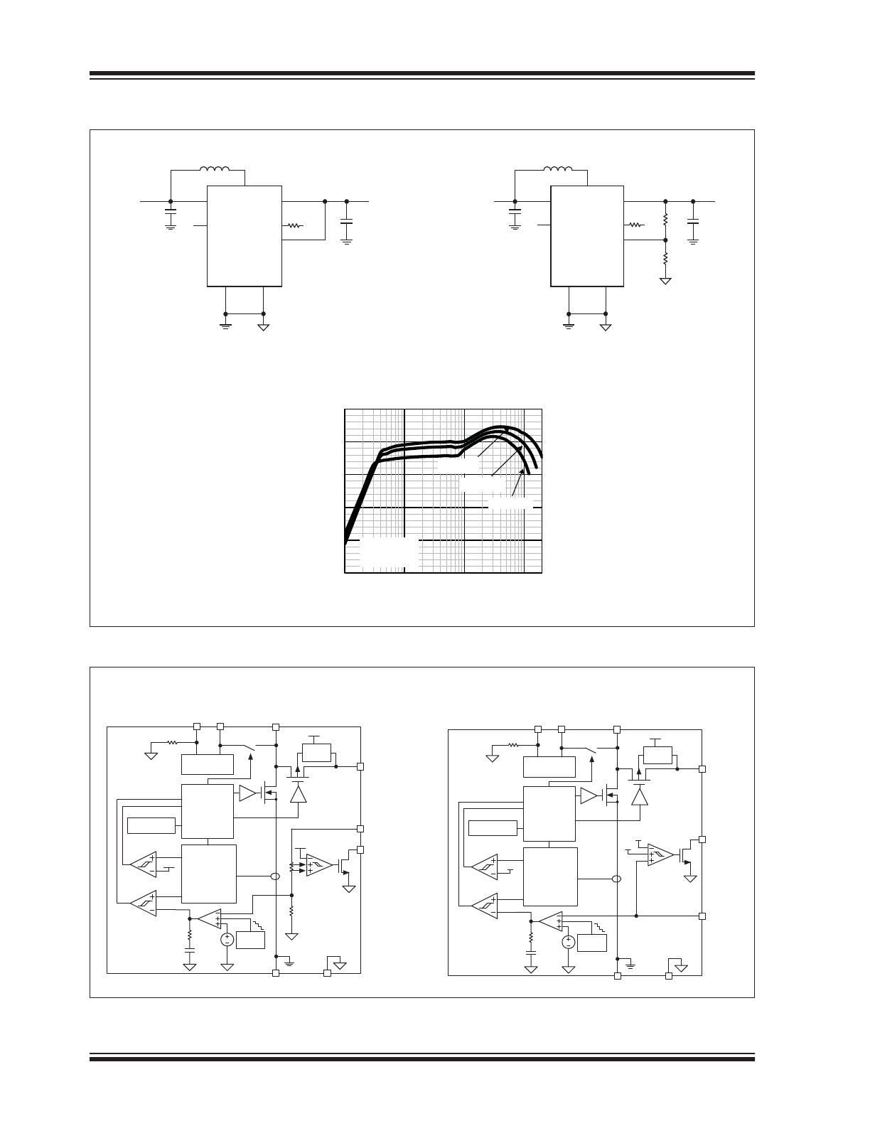
Typical Application Schematics
Functional Block Diagrams
AGND
SW
IN
EN
PGND
OUT
/PG
FB
V
IN
V
OUT
5.0V
L1 1μH
2.5V to 5.0V
C1
4.7μF
10V
V
IN
R1
1MΩ
R2
910kΩ
R3
200kΩ
C2*
22μF
10V
MIC2875 (Adjustable Output)
MIC2875 (Fixed Output)
AGND
SW
V
IN
IN
EN
PGND
OUT
/PG
OUTS
V
OUT
5.0V
L1 1μH
2.5V to 5.0V
C1
4.7μF
10V
V
IN
R1
1MΩ
C2*
22μF
10V
* Two more 22
F capacitors should be added in parallel with C2 for V
IN
> 5.0V.
50
60
70
80
90
100
0.001
0.010
0.100
1.000
EFFICIENCY
(%
)
LOAD CURRENT (A)
V
IN
= 3.6V
V
IN
= 3.0V
V
IN
= 2.5V
V
OUT
= 5.0V
L = 1μH
C
OUT
= 22μF
Efficiency vs. Load Current
MIC2875 (Fixed Output)
MIC2875 (Adj. Output)
EN
IN
SW
ANTI-
RINGING
REFERENCE
GENERATOR
2MHz
OSCILLATOR
OC
4.8A
PWM LOGIC
CONTROL
+
MINIMUM
SWITCHING
CURRENT
SENSE
+
SLOPE
COMPENSATION
VIN
OUT
BODY
DRIVER
HS
DRIVER
LS
DRIVER
/PG
PGND
AGND
VREF
SOFT-
START
PWM
OUTS
VIN
EN
IN
SW
ANTI-
RINGING
REFERENCE
GENERATOR
2MHz
OSCILLATOR
OC
4.8A
PWM LOGIC
CONTROL
+
MINIMUM
SWITCHING
CURRENT
SENSE
+
SLOPE
COMPENSATION
VIN
OUT
BODY
DRIVER
HS
DRIVER
LS
DRIVER
PGL
PGH
/PG
FB
PGND
AGND
VREF
SOFT-
START
PWM

2015 Microchip Technology Inc.
DS20005549A-page 3
MIC2875
1.0
ELECTRICAL CHARACTERISTICS
Absolute Maximum Ratings †
IN, EN, OUT, FB, /PG to PGND ................................................................................................................... –0.3V to +6V
AGND to PGND......................................................................................................................................... –0.3V to +0.3V
Power Dissipation ....................................................................................................................Internally Limited (
Note 1
)
ESD Rating (
Note 2
) ................................................................................................................ ±1.5 kV HBM, ±200V MM
Operating Ratings ††
Supply Voltage (V
IN
)
.............................................................................................................................. +2.5V to +5.5V
Output Voltage (V
OUT
) ................................................................................................................................... Up to +5.5V
Enable Voltage (V
EN
) ....................................................................................................................................... 0V to +V
IN
†
Notice: Exceeding the absolute maximum ratings may damage the device.
†† Notice:
The device is not guaranteed to function outside its operating ratings.
Note 1:
The maximum allowable power dissipation of any T
A
(ambient temperature) is P
D(max)
= (T
J(max)
– T
A
) / ϴ
JA
.
Exceeding the maximum allowable power dissipation will result in excessive die temperature, and the reg-
ulator will go into thermal shutdown
2:
Devices are ESD sensitive. Handling precautions are recommended. Human body model, 1.5 kΩ
in series with 100 pF
.
MIC2875
DS20005549A-page 4
2015 Microchip Technology Inc.
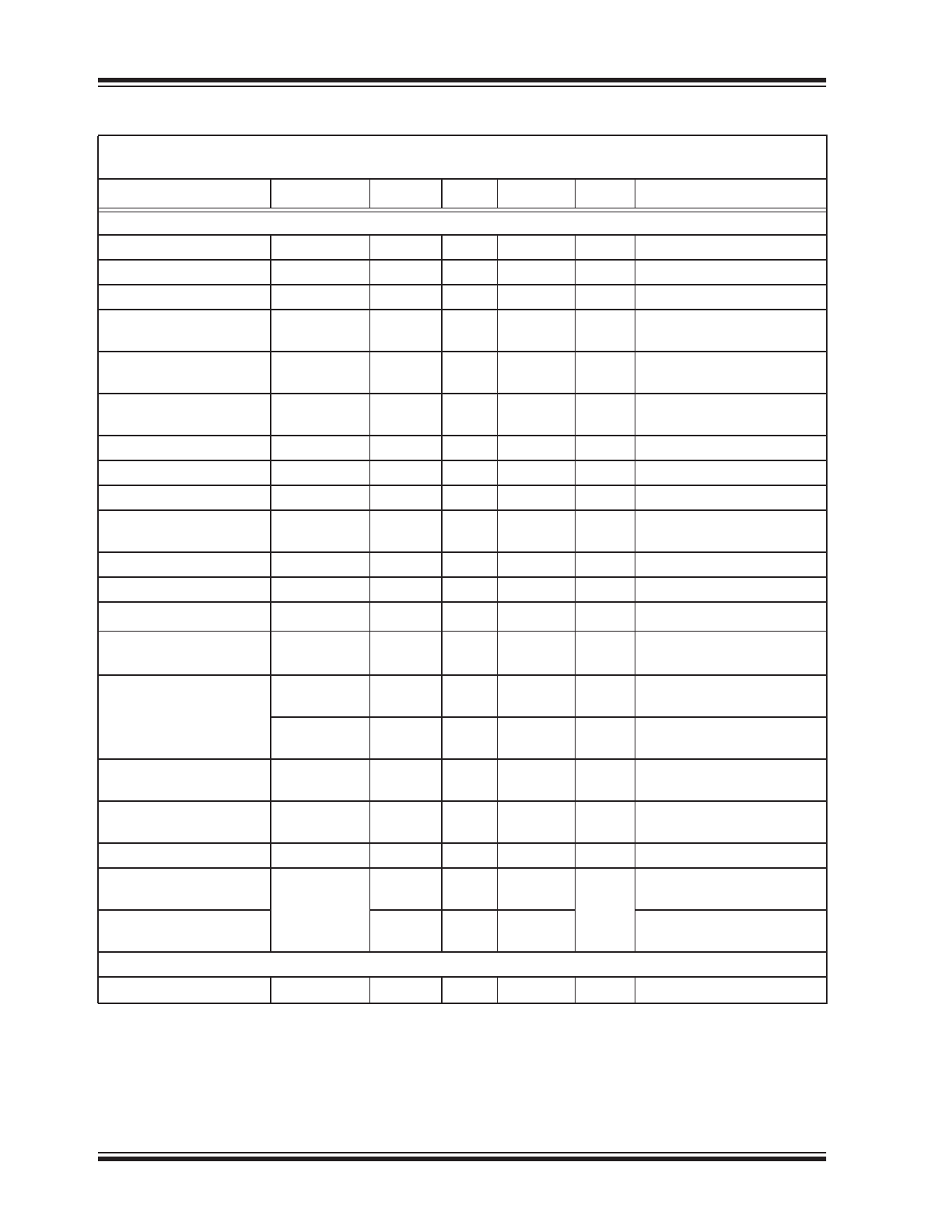
TABLE 1-1:
ELECTRICAL CHARACTERISTICS (
Note 1
)
Electrical Characteristics:
V
IN
= 3.6V, V
OUT
= 5V, C
IN
= 4.7 μF, C
OUT
= 22 μF, L = 1 μH T
A
= 25°C, bold values are
valid for –40°C
T
J
+125°C Unless otherwise indicated.
Parameters
Sym.
Min.
Typ.
Max.
Units
Conditions
Power Supply
Supply Voltage Range
V
IN
2.5
—
5.5
V
—
UVLO Rising Threshold
V
UVLOR
—
2.32
2.49
V
—
UVLO Hysteresis
V
UVLOH
—
200
—
mV
—
Quiescent Current
I
VIN
—
1
—
mA
Operating at minimum
switching frequency
V
IN
Shutdown Current
I
VINSD
—
1
3
μA
V
EN
= 0V, V
IN
= 5.5V, V
OUT
=
0V
V
OUT
Shutdown Current
I
VOUTSD
—
2
5
μA
V
EN
= 0V, V
IN
= 0.3V, V
OUT
=
5.5V
Output Voltage
V
OUT
V
IN
—
5.5
V
—
Feedback Voltage
V
FB
0.8865
0.9
0.9135
V
Adjustable version, I
OUT
= 0A
Voltage Accuracy
—
1.5
—
+1.5
%
Fixed version, I
OUT
= 0A
Line Regulation
—
—
0.3
—
%/V
2.5V < V
IN
< 4.5V, I
OUT
=
500 mA
Load Regulation
—
—
0.2
—
%/A
I
OUT
= 200 mA to 1200 mA
Maximum Duty Cycle
D
MAX
—
92
—
%
—
Minimum Duty Cycle
D
MIN
—
6.5
—
%
—
Low-side Switch Current
Limit
I
LS
3.8
4.8
5.8
A
V
IN
= 2.5V
Switch On-Resistance
PMOS
—
79
—
mΩ
V
IN
= 3.0V, I
SW
= 200 mA,
V
OUT
= 5.0V
NMOS
—
82
—
mΩ
V
IN
= 3.0V, I
SW
= 200 mA,
V
OUT
= 5.0V
Switch Leakage Current
(
Note 2
)
I
SW
—
0.2
5
μA
V
EN
= 0V, V
IN
= 5.5V
Minimum Switching
Frequency
F
SWMIN
—
45
—
kHz
I
OUT
= 0 mA
Oscillator Frequency
F
OSC
1.6
2
2.4
MHz
—
Overtemperature
Shutdown Threshold
T
SD
—
155
—
°C
—
Overtemperature
Shutdown Hysteresis
—
15
—
—
Soft-Start
Soft-Start Time
T
SS
—
1.1
—
ms
V
OUT
= 5.0V
Note 1:
Specification for packaged product only.
2:
Guaranteed by design and characterization.

2015 Microchip Technology Inc.
DS20005549A-page 5
MIC2875
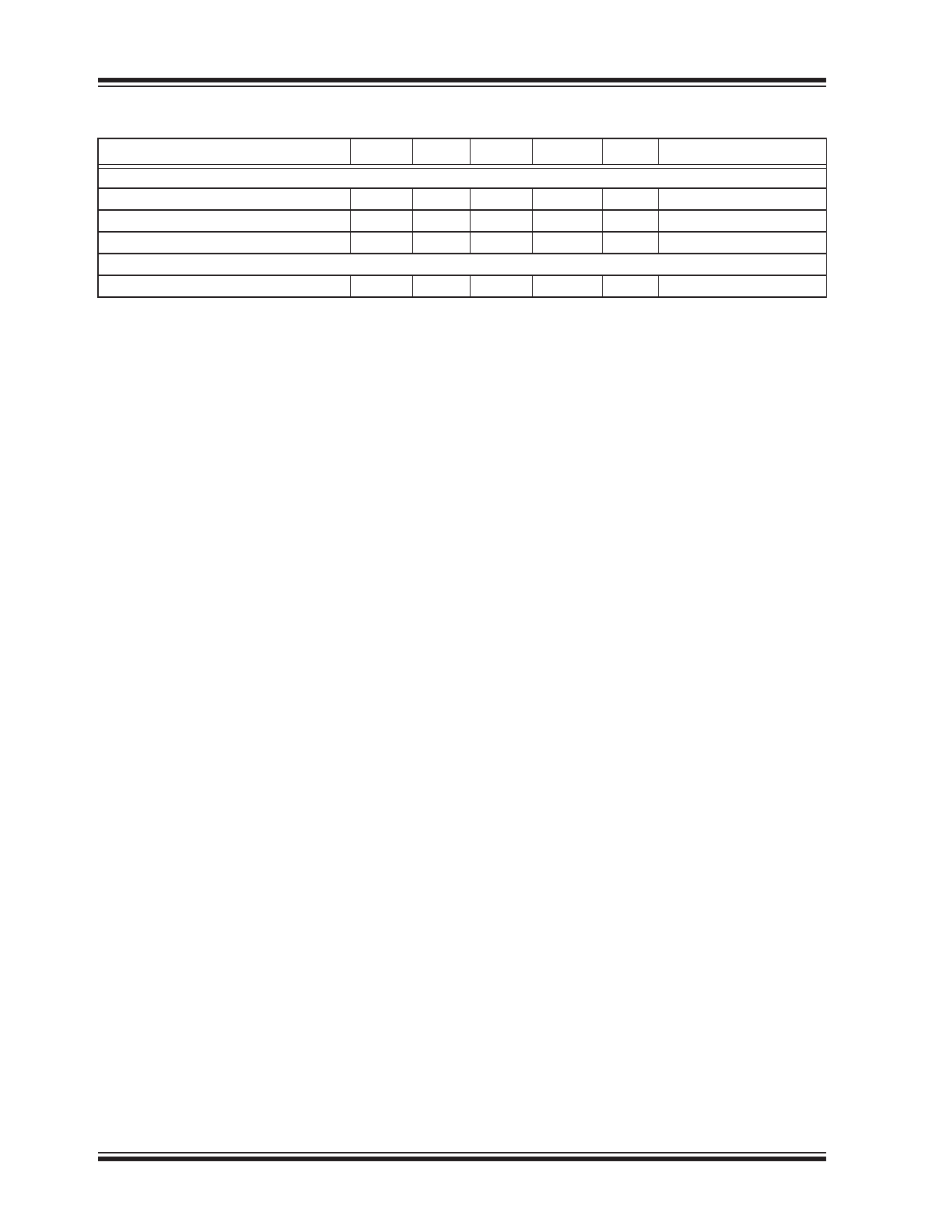
EN, /PG Control Pins
EN Threshold Voltage
V
EN
1.5
—
—
V
Boost converter and chip logic
ON
—
—
0.4
Boost converter and chip logic
OFF
EN Pin Current
—
—
1.5
3
μA
V
IN
= V
EN
= 3.6V
Power-Good Threshold
(Rising)
V
/PG-THR
—
0.90 ×
V
OUT
—
V
—
Power-Good Threshold
(Falling)
V
/PG-THF
—
0.83 ×
V
OUT
—
V
—
TABLE 1-1:
ELECTRICAL CHARACTERISTICS (CONTINUED)(
Note 1
)
Electrical Characteristics:
V
IN
= 3.6V, V
OUT
= 5V, C
IN
= 4.7 μF, C
OUT
= 22 μF, L = 1 μH T
A
= 25°C, bold values are
valid for –40°C
T
J
+125°C Unless otherwise indicated.
Parameters
Sym.
Min.
Typ.
Max.
Units
Conditions
Note 1:
Specification for packaged product only.
2:
Guaranteed by design and characterization.
MIC2875
DS20005549A-page 6
2015 Microchip Technology Inc.
TEMPERATURE SPECIFICATIONS (
Note 1
)
Parameters
Sym.
Min.
Typ.
Max.
Units
Conditions
Temperature Ranges
Lead Temperature
—
—
260
—
°C
Soldering 10s
Storage Temperature Range
T
S
–65
—
+150
°C
—
Junction Operating Temperature
T
J
–40
—
+125
°C
—
Package Thermal Resistances
Thermal Resistance, TDFN-22-8Ld
JA
—
90
—
°C/W
—
Note 1:
The maximum allowable power dissipation is a function of ambient temperature, the maximum allowable
junction temperature and the thermal resistance from junction to air (i.e., T
A
, T
J
,
JA
). Exceeding the
maximum allowable power dissipation will cause the device operating junction temperature to exceed the
maximum +125°C rating. Sustained junction temperatures above +125°C can impact the device reliability.
2015 Microchip Technology Inc.
DS20005549A-page 7
MIC2875
2.0
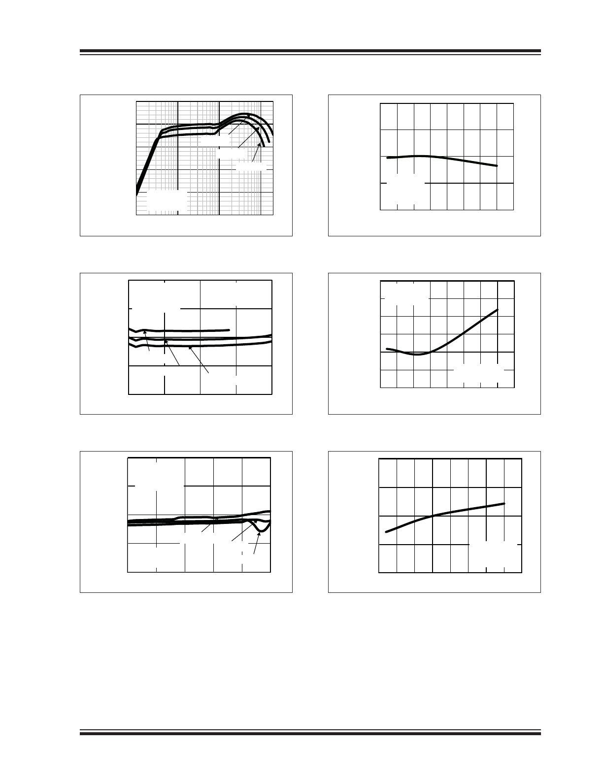
TYPICAL PERFORMANCE CURVES
FIGURE 2-1:
Efficiency vs. Load Current.
FIGURE 2-2:
Output Voltage vs. Load
Current.
FIGURE 2-3:
Output Voltage vs. Input
Voltage.
FIGURE 2-4:
Oscillator Frequency vs.
Temperature.
FIGURE 2-5:
Output Shutdown Current
vs. Temperature.
FIGURE 2-6:
Feedback Voltage vs.
Temperature.
50
60
70
80
90
100
0.001
0.010
0.100
1.000
EFFICIENCY
(%
)
LOAD CURRENT (A)
V
IN
= 3.6V
V
IN
= 3.0V
V
IN
= 2.5V
V
OUT
= 5.0V
L = 1μH
C
OUT
= 22μF
4.90
4.95
5.00
5.05
5.10
0.0
0.5
1.0
1.5
2.0
OUTPUT VOL
TA
G
E
(V
)
LOAD CURRENT (A)
V
IN
= 3.5V
V
OUT
= 5.0V
L = 1μH
C
OUT
= 22μF
T
A
= 125℃
T
A
= -40℃
ADJUSTABLE
R2 = 910kΩ
R3 = 200kΩ
T
A
= 25℃
4.80
4.90
5.00
5.10
5.20
2.5
3.0
3.5
4.0
4.5
5.0
O
UT
PU
T V
O
LTA
G
E
(V
)
INPUT VOLTAGE(V)
V
OUT
= 5.0V
L = 1μH
C
OUT
= 22μF
I
OUT
= 500mA
ADJUSTABLE
R2 = 910kΩ
R3 = 200kΩ
T
A
= 125℃
T
A
= 25℃
T
A
= -40℃
1.96
1.98
2.00
2.02
2.04
-50
-25
0
25
50
75
100
125
150
OSCILLA
TO
R FREQUENCY
(MHz)
TEMPERATURE (℃)
V
IN
= 3.6V
V
OUT
= 5.0V
L = 1μH
C
OUT
= 22μF
I
OUT
= 0A
1.00
1.50
2.00
2.50
3.00
3.50
4.00
-50
-25
0
25
50
75
100
125
150
SHUTDOW
N CURRENT (µA
)
TEMPERATURE (℃)
V
EN
= 0V
V
IN
= 0.3V
V
OUT
= 5.5V
ADJUSTABLE
R2 = 910kΩ
R3 = 200kΩ
0.896
0.898
0.900
0.902
0.904
-50
-25
0
25
50
75
100
125
150
FEEDBA
CK VOL
TA
GE
(V
)
TEMPERATURE (℃)
ADJUSTABLE
V
OUT
= 5.0V
R2 = 910kΩ
R3 = 200kΩ
MIC2875
DS20005549A-page 8
2015 Microchip Technology Inc.
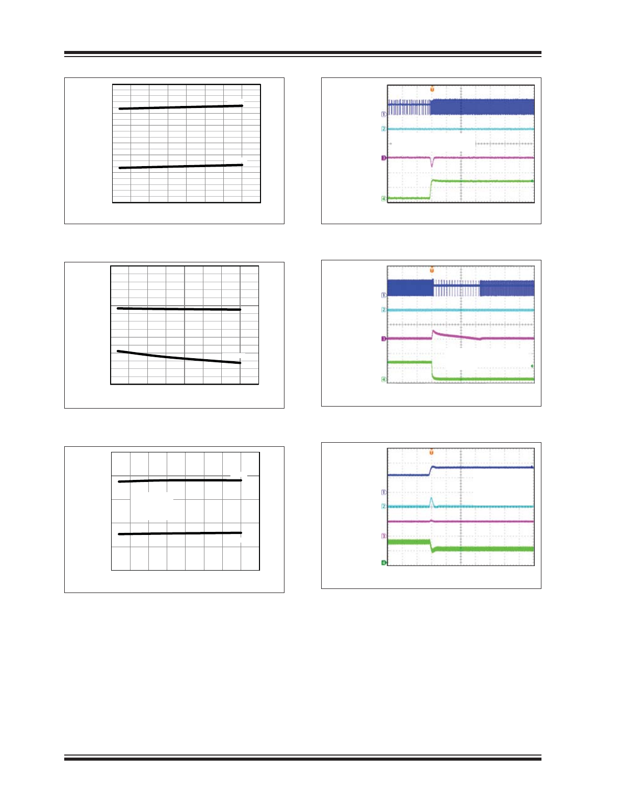
FIGURE 2-7:
UVLO Threshold vs.
Temperature.
FIGURE 2-8:
Enable Threshold vs.
Temperature.
FIGURE 2-9:
Power Good Threshold vs.
Temperature.
FIGURE 2-10:
Load Transient (0A to 1.2A).
.
FIGURE 2-11:
Load Transient (1.2A to 0A).
.
FIGURE 2-12:
Line Transient (2.5V to
3.5V).
2.00
2.10
2.20
2.30
2.40
-50
-25
0
25
50
75
100
125
150
INPUT VOL
TA
GE
(V
)
TEMPERATURE (℃)
RISING
FALLING
0.60
0.80
1.00
1.20
-50
-25
0
25
50
75
100
125
150
ENA
B
LE THRESHOLD
VOL
TA
GE
(V
)
TEMPERATURE (℃)
RISING
FALLING
3.80
4.00
4.20
4.40
4.60
4.80
-50
-25
0
25
50
75
100
125
150
POWER GOOD THRESHOLD
VOL
TA
G
E
(V
)
TEMPERATURE (℃)
RISING
FALLING
ADJUSTABLE
R2 = 910kΩ
R3 = 200kΩ
V
OUT
= 5.0V
V
IN
= 3.5V, V
OUT
= 5.0V
L
= 1μH, I
OUT
= 0A TO 1.2A
Time (100μs/div)
I
OUT
(1A/div)
V
SW
(5V/div)
V
/PG
(2V/div)
V
OUT
(1V/div)
(AC-COUPLED)
Time (100μs/div)
I
OUT
(1A/div)
V
SW
(5V/div)
V
/PG
(2V/div)
V
OUT
(1V/div)
(AC-COUPLED)
V
IN
= 3.5V, V
OUT
= 5.0V
L
= 1μH, I
OUT
= 1.2A TO 0A
Time (100μs/div)
I
L
(2A/div)
V
IN
(2V/div)
V
OUT
(5V/div)
V
OUT
(500mV/div)
(AC-COUPLED)
V
IN
= 2.5V TO 3.5V
V
OUT
= 5.0V
L
= 1μH
I
OUT
= 1A
2015 Microchip Technology Inc.
DS20005549A-page 9
MIC2875
.
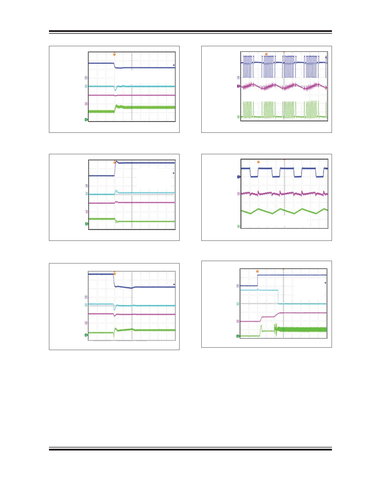
FIGURE 2-13:
Line Transient (3.5V to
2.5V).
.
FIGURE 2-14:
Line Transient (2.5V to
5.5V).
FIGURE 2-15:
Line Transient (5.5V to
2.5V).
FIGURE 2-16:
Output Ripple (Pulse Skipping
Mode).
FIGURE 2-17:
Output Ripple (PWM Mode).
FIGURE 2-18:
Soft–Start (Boost Mode).
Time (100μs/div)
I
L
(2A/div)
V
IN
(2V/div)
V
OUT
(5V/div)
V
OUT
(500mV/div)
(AC-COUPLED)
V
IN
= 3.5V TO 2.5V, V
OUT
= 5.0V
L
= 1μH, I
OUT
= 1A
Time (100μs/div)
I
L
(5A/div)
V
IN
(2V/div)
V
OUT
(5V/div)
V
OUT
(2V/div)
(AC-COUPLED)
V
IN
= 2.5V TO 5.5V
V
OUT
= 5.0V
L
= 1μH
I
OUT
= 1A
Time (100μs/div)
I
L
(5A/div)
V
IN
(2V/div)
V
OUT
(5V/div)
V
OUT
(2V/div)
(AC-COUPLED)
V
IN
= 5.5V TO 2.5V
V
OUT
= 5.0V, L
= 1μH
I
OUT
= 1A
PULSE SKIPPING MODE
V
IN
= 3.5V, V
OUT
= 5.0V, I
OUT
= 50mA
Time (4μs/div)
I
L
(200mA/div)
V
SW
(2V/div)
V
OUT
(50mV/div)
(AC-COUPLED)
PWM MODE
V
IN
= 3.5V, V
OUT
= 5.0V, I
OUT
= 1.2A
Time (200ns/div)
I
L
(1A/div)
V
SW
(5V/div)
V
OUT
(50mV/div)
(AC-COUPLED)
BOOST MODE
V
IN
= 3.5V
V
OUT
= 5.0V
I
OUT
= 500mA
Time (400μs/div)
I
L
(1A/div)
V
EN
(2V/div)
V
/PG
(2V/div)
V
OUT
(5V/div)
MIC2875
DS20005549A-page 10
2015 Microchip Technology Inc.
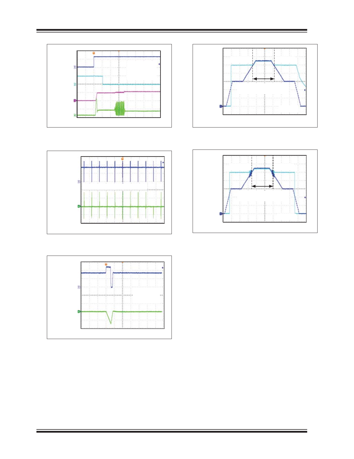
FIGURE 2-19:
Soft–Start Bypass Mode.
FIGURE 2-20:
Minimum Switching.
FIGURE 2-21:
Minimum Switching
(Zoom–In).
FIGURE 2-22:
Bypass mode.
FIGURE 2-23:
Bypass Mode.
BYPASS MODE
V
IN
= 5.5V
V
OUT
= 5.0V
I
OUT
= 500mA
Time (400μs/div)
I
L
(1A/div)
V
EN
(2V/div)
V
/PG
(5V/div)
V
OUT
(5V/div)
V
IN
= 3.5V, F
SWMIN
= 45kHz, I
OUT
= 0A
Time (20μs/div)
I
L
(200mA/div)
V
SW
(2V/div)
Time (400ns/div)
I
L
(200mA/div)
V
SW
(2V/div)
V
IN
= 3.5V
F
SWMIN
= 45kHz
I
OUT
= 0A
Time (1s/div)
V
IN
(1V/div)
V
OUT
(1V/div)
BYPASS MODE – V
IN
> 5.0V
V
OUT
= V
IN
I
OUT
= 0A
V
OUT
= 5.0V
V
OUT
= 5.0V
Time (1s/div)
V
IN
(1V/div)
V
OUT
(1V/div)
BYPASS MODE – V
IN
> 5.0V
V
OUT
= V
IN
I
OUT
= 500mA
V
OUT
= 5.0V
V
OUT
= 5.0V