
2017 Microchip Technology Inc.
DS20005725B-page 1
MIC2544/48
Features
• 2.7V to 5.5V Input
• Adjustable Current-Limit up to 1.5A
• Reverse Current Flow Blocking (No “Body Diode”)
• 75 μA Typical On-State Supply Current
• 1 μA Typical Off-State Supply Current
• 120 mΩ Maximum On-Resistance
• Open-Drain Fault Flag
• Thermal Shutdown
• Thermal Shutdown Output Latch (MIC2548)
• 2 ms (Slow) Turn-On and Fast Turn-Off
• Available with Active-High or Active-Low Enable
Applications
• USB Power Distribution
• PCI Bus Power Switching
• Notebook PC
• ACPI Power Distribution
• PC Card Hot Swap Applications
• Inrush Current-Limiting
General Description
The MIC2544 and MIC2548 are integrated, high-side
power switches optimized for low-loss DC power
switching and other power management applications,
including Advanced Configuration and Power Interface
(ACPI). The MIC2544/48 are cost-effective, highly
integrated solutions that require few external
components to satisfy USB and ACPI requirements.
Load current management features include a precision
resistor-programmable output current-limit and a
soft-start circuit that minimizes inrush current when the
switch is enabled. Thermal shutdown, along with
current-limit, protects the switch and the attached
device.
The MIC2544/48’s open-drain flag output is used to
indicate current-limiting or thermal shutdown to a local
controller. The MIC2548 has an additional internal latch
that turns the output off upon thermal shutdown,
providing robust fault control. The enable signal is
compatible with both 3V and 5V logic, and is also used
as the thermal shutdown latch reset for the MIC2548.
The MIC2544 and MIC2548 are available in active-high
and active-low enable versions in the 8-pin SOIC and
8-pin MSOP packages.
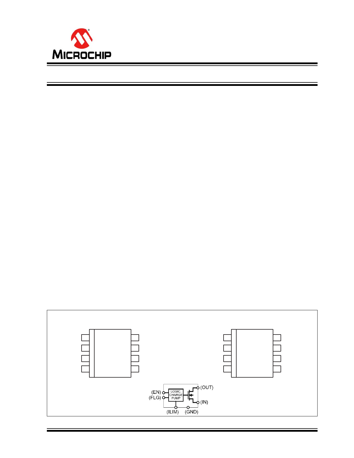
Package Types
MIC2544/MIC2548
8-P
IN
SOIC (M)
MIC2544/MIC2548
8-P
IN
MSOP (MM)
1
EN
FLG
GND
ILIM
8 OUT
IN
OUT
NC
7
6
5
2
3
4
1
EN
FLG
GND
NC
8 OUT
IN
OUT
ILIM
7
6
5
2
3
4
Programmable Current-Limit High-Side Switch
MIC2544/48
DS20005725B-page 2
2017 Microchip Technology Inc.
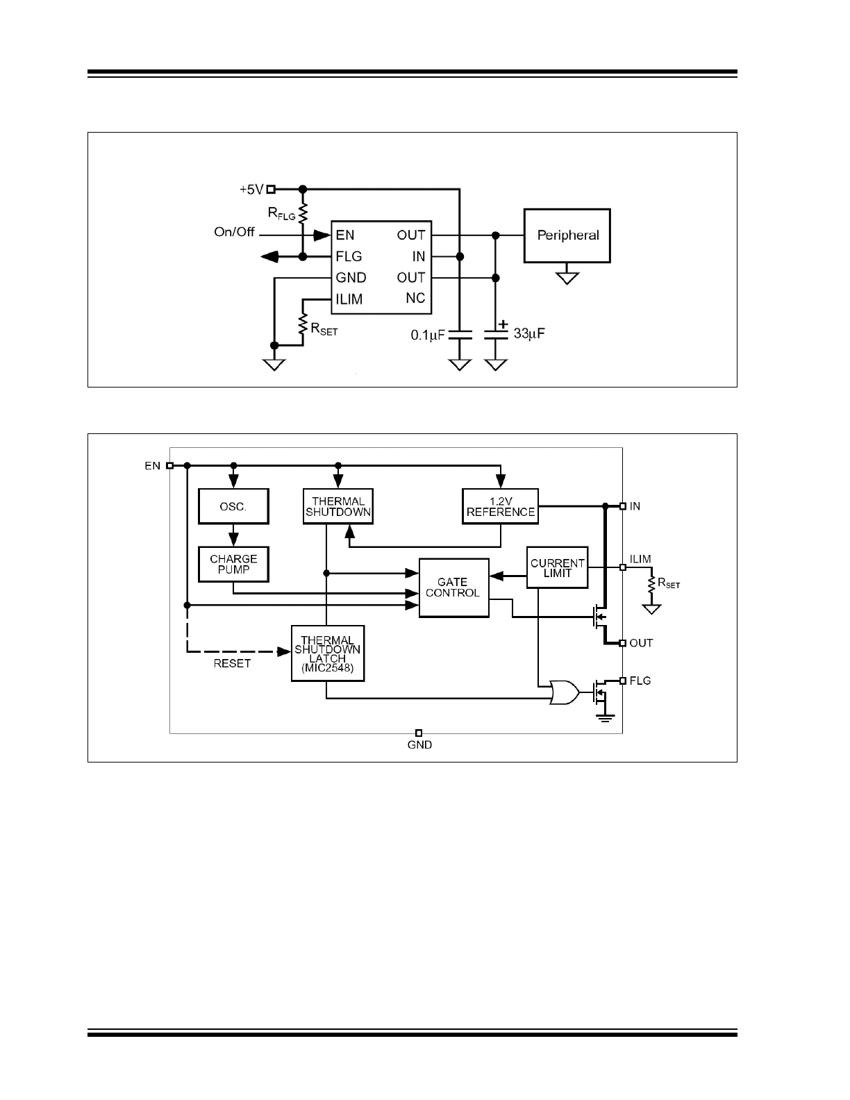
Typical Application Circuit
Functional Diagram
T
YPICAL
A
DVANCED
C
ONFIGURATION
AND
P
OWER
I
NTERFACE
(ACPI) A
PPLICATION
MIC2544-xYM
SOIC Pinout Shown

2017 Microchip Technology Inc.
DS20005725B-page 3
MIC2544/48
1.0
ELECTRICAL CHARACTERISTICS
Absolute Maximum Ratings †
Supply Voltage (V
IN
) ................................................................................................................................................+7.0V
Output Voltage (V
OUT
) .............................................................................................................................. –0.3V to +7.0V
Output Current (I
OUT
)............................................................................................................................. Internally Limited
Enable Input (V
EN
) ............................................................................................................................... –0.3V to V
IN
+0.3V
Fault Flag Voltage (V
FLG
).........................................................................................................................................+7.0V
Fault Flag Current (I
FLG
) .........................................................................................................................................50 mA
ESD Rating (
Note 1
) .................................................................................................................................................. 2 kV
Operating Ratings ‡
Supply Voltage (V
IN
) ................................................................................................................................. +2.7V to +5.5V
Current Limit Set Range ............................................................................................................................... 0.1A to 1.5A
†
Notice: Stresses above those listed under “Absolute Maximum Ratings” may cause permanent damage to the device.
This is a stress rating only and functional operation of the device at those or any other conditions above those indicated
in the operational sections of this specification is not intended. Exposure to maximum rating conditions for extended
periods may affect device reliability.
‡ Notice:
The device is not guaranteed to function outside its operating ratings.
Note 1:
Devices are ESD sensitive. Handling precautions recommended. Human body model, 1.5 kΩ in series with
100 pF.
MIC2544/48
DS20005725B-page 4
2017 Microchip Technology Inc.
TABLE 1-1:
ELECTRICAL CHARACTERISTICS (
Note 1
)
Electrical Characteristics:
V
IN
= +5V; T
A
= 25°C, bold values indicate –40°C to +85°C, unless noted.
Parameter
Symbol
Min.
Typ.
Max.
Units
Conditions
Supply Current
I
IN
—
0.75
5
µA
Switch off, OUT = Open (
Note 2
)
—
75
160
Switch on, OUT = Open (
Note 2
)
Enable Input Voltage
V
EN
2.4
1.7
—
V
Enable High, (
Note 2
)
—
1.5
0.8
Enable Low, (
Note 2
)
Enable Input
Capacitance
—
—
1
—
pF
Note 3
Switch Resistance
R
DS(ON)
—
80
120
mΩ
I
OUT
= 500 mA
Current Limit Factor
—
184
230
276
V
I
OUT
= 100 mA to 1A, V
OUT
= 1V to 4V,
(
Note 4
)
161
230
299
I
OUT
= 500 mA to 1.5A, V
OUT
= 1V to
4V, (
Note 4
)
Output Leakage Current
—
—
1
10
µA
Switch off
Output Turn-On Delay
t
ON
1
2
5
ms
R
L
= 10Ω, C
L
= 1 µF,
Figure 4-2
,
Figure 4-3
Output Turn-On Rise
Time
t
R
1
2
5
ms
R
L
= 10Ω, C
L
= 1 µF,
Figure 4-2
,
Figure 4-3
Output Turn-Off Delay
t
OFF
—
22
—
µs
R
L
= 10Ω, C
L
= 1 µF,
Figure 4-2
,
Figure 4-3
Output Turn-Off Fall Time
t
F
—
21
—
µs
R
L
= 10Ω, C
L
= 1 µF,
Figure 4-2
,
Figure 4-3
Overtemperature
Threshold Shutdown
—
—
140
—
°C
T
J
increasing
—
130
—
T
J
decreasing
Error Flag Output
Resistance
—
—
4
15
Ω
V
IN
= 5V, I
L
= 10 μA
—
5
20
V
IN
= 3.3V, I
L
= 10 μA
Error Flag Off Current
—
—
0.01
1
µA
V
FLG
= 5V
EN Pulse Reset Width
—
5
—
—
µs
MIC2548 thermal shutdown latch
V
IN
to EN Set-Up
—
0
—
—
µs
MIC2548, (
Note 4
)
Current-Limit Response
Time
—
—
25
—
µs
V
OUT
= 0V, (
Note 4
)
Overcurrent Flag
Response Time
—
—
5
—
µs
V
OUT
= V
IN
/2 to FLG low.
Note 1:
Specification for packaged product only.
2:
Off is ≤ 0.8V and on is ≥ 2.4V for the MIC2544-1 and MIC2548-1. Off is ≥ 2.4V and on is ≤ 0.8V for the
MIC2544-2 and MIC2548-2. The enable input has about 200 mV of hysteresis.
3:
Guaranteed by design but not production tested.
4:
Current limit threshold is determined by I
LIMIT
= 230V/R
SET
, where R
SET
is in ohms.
2017 Microchip Technology Inc.
DS20005725B-page 5
MIC2544/48
TEMPERATURE SPECIFICATIONS (
Note 1
)
Parameters
Sym.
Min.
Typ.
Max.
Units
Conditions
Temperature Ranges
Storage Temperature Range
T
S
–65
—
+150
°C
—
Lead Temperature
—
—
—
+260
°C
Soldering, 5 sec.
Junction Temperature
T
J
—
—
—
°C
Internally Limited
Ambient Temperature
T
A
–40
—
+85
°C
—
Package Thermal Resistance
Thermal Resistance, 8-Ld SOIC
θ
JA
—
160
—
°C/W
—
Thermal Resistance, 8-Ld MSOP
θ
JA
—
206
—
°C/W
—
Note 1:
The maximum allowable power dissipation is a function of ambient temperature, the maximum allowable
junction temperature and the thermal resistance from junction to air (i.e., T
A
, T
J
,
JA
). Exceeding the
maximum allowable power dissipation will cause the device operating junction temperature to exceed the
maximum +125°C rating. Sustained junction temperatures above +125°C can impact the device reliability.
MIC2544/48
DS20005725B-page 6
2017 Microchip Technology Inc.
2.0
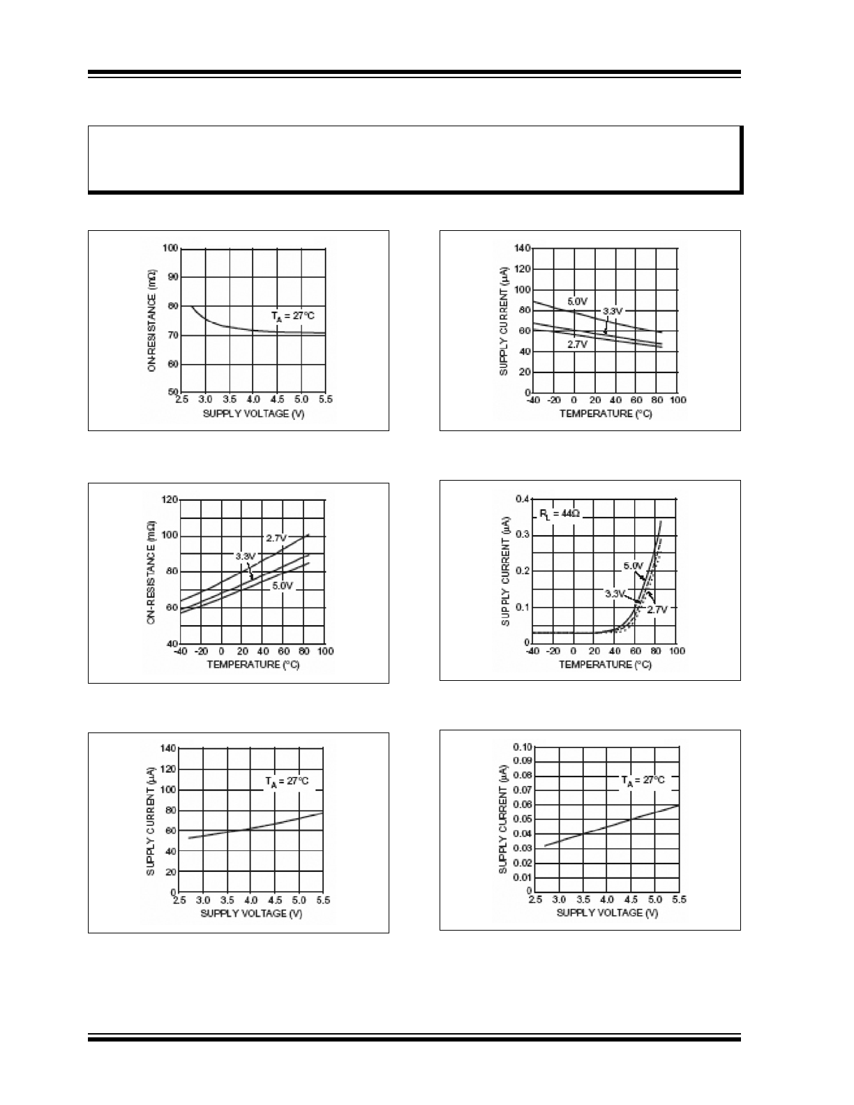
TYPICAL PERFORMANCE CURVES
FIGURE 2-1:
Output On-Resistance vs.
Supply Voltage.
FIGURE 2-2:
Output On-Resistance vs.
Temperature.
FIGURE 2-3:
On-State Supply Current vs.
Supply Voltage.
FIGURE 2-4:
On-State Supply Current vs.
Temperature.
FIGURE 2-5:
Off-State Supply Current vs.
Temperature.
FIGURE 2-6:
Off-State Supply Current vs.
Supply Voltage.
Note:
The graphs and tables provided following this note are a statistical summary based on a limited number of
samples and are provided for informational purposes only. The performance characteristics listed herein
are not tested or guaranteed. In some graphs or tables, the data presented may be outside the specified
operating range (e.g., outside specified power supply range) and therefore outside the warranted range.
2017 Microchip Technology Inc.
DS20005725B-page 7
MIC2544/48
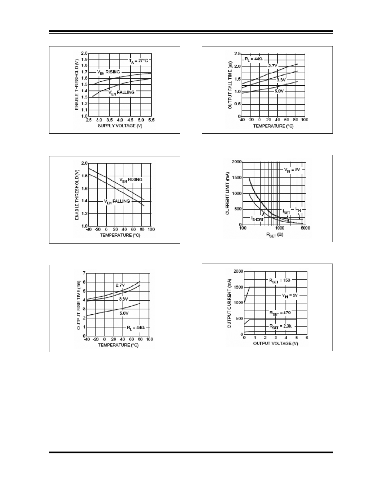
FIGURE 2-7:
Enable Threshold Voltage
vs. Supply Voltage.
FIGURE 2-8:
Enable Threshold Voltage
vs. Temperature.
FIGURE 2-9:
Rise Time vs. Temperature.
FIGURE 2-10:
Output Fall Time vs.
Temperature.
FIGURE 2-11:
Current Limit vs. R
SET
.
FIGURE 2-12:
Output Current vs. Output
Voltage.
MIC2544/48
DS20005725B-page 8
2017 Microchip Technology Inc.
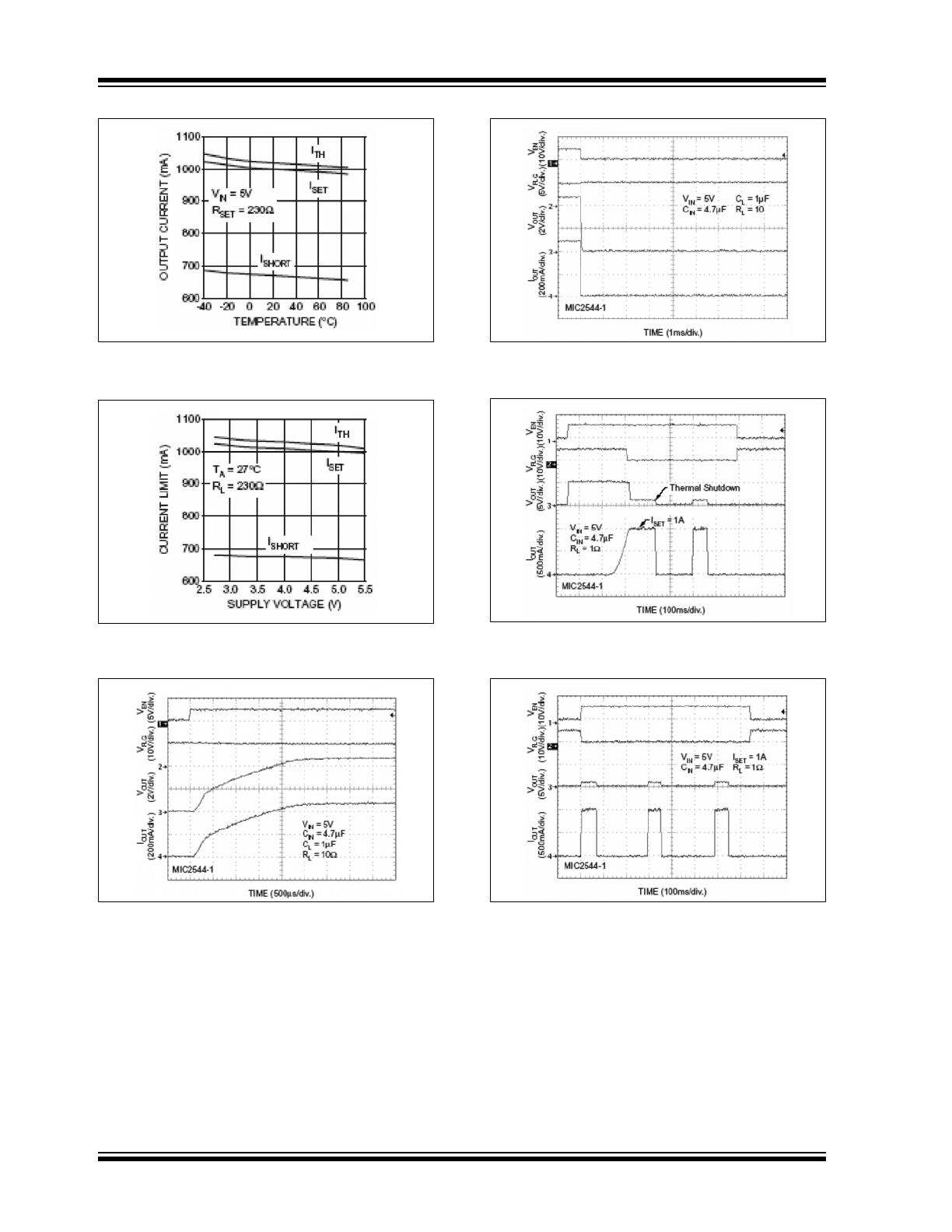
FIGURE 2-13:
Current Limit vs.
Temperature.
FIGURE 2-14:
Current Limit vs. Supply
Voltage.
FIGURE 2-15:
Turn-On Response.
FIGURE 2-16:
Turn-Off Response.
FIGURE 2-17:
Current-Limit Response.
FIGURE 2-18:
Enable Into Heavy Load.
2017 Microchip Technology Inc.
DS20005725B-page 9
MIC2544/48
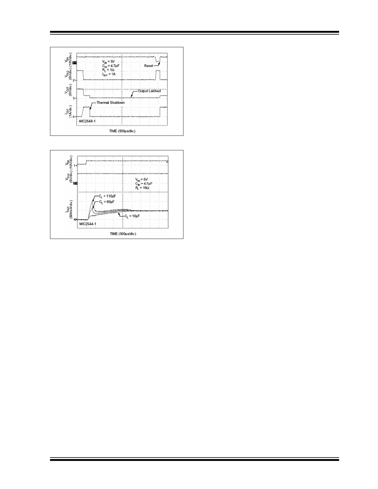
FIGURE 2-19:
Enable Into Heavy Load.
FIGURE 2-20:
Inrush Current Response.
MIC2544/48
DS20005725B-page 10
2017 Microchip Technology Inc.
3.0
PIN DESCRIPTIONS
The descriptions of the pins are listed in
Table 3-1
.
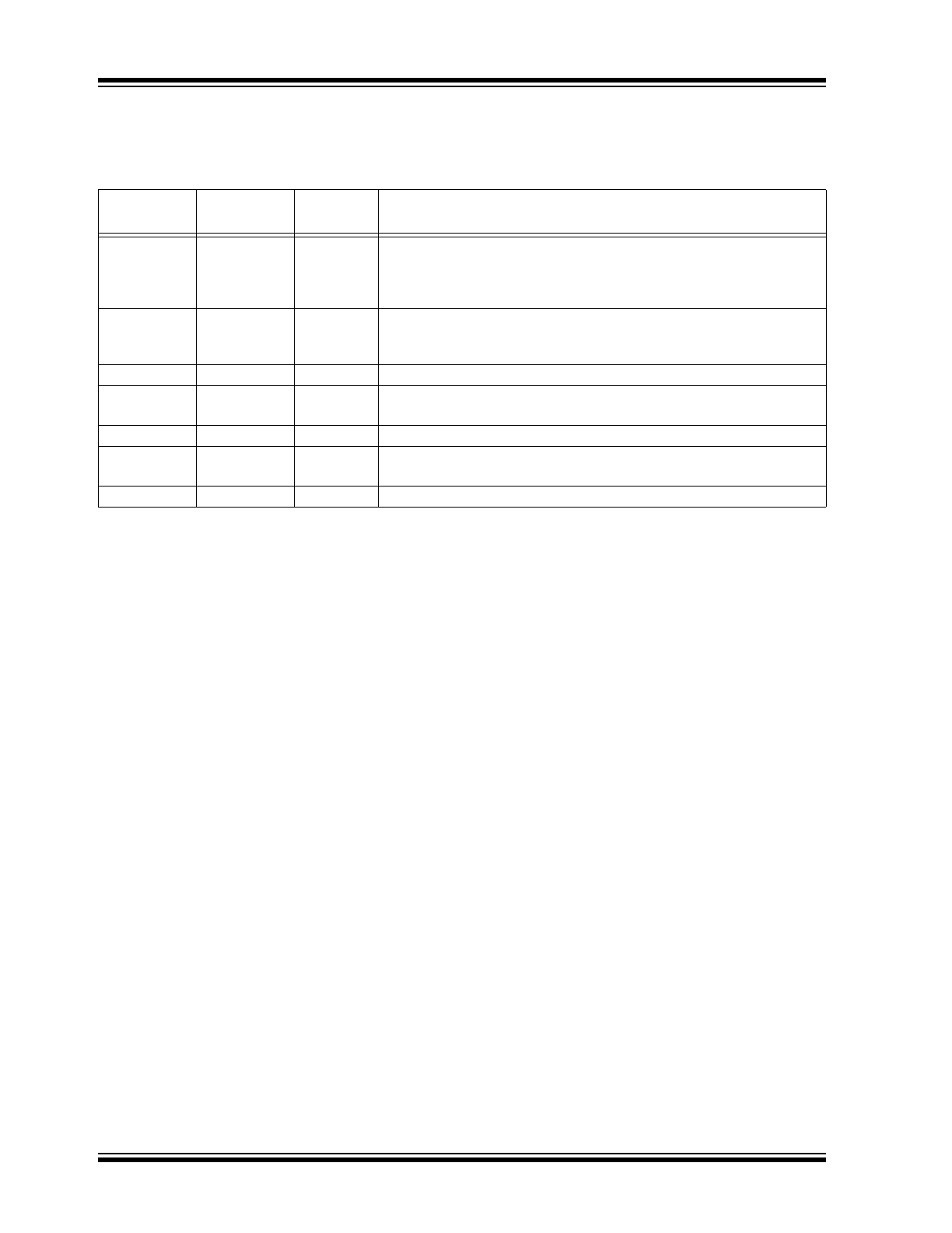
TABLE 3-1:
PIN FUNCTION TABLE
Pin Number
8-Pin MSOP
Pin Number
8-Pin SOIC
Pin Name
Description
1
1
EN
Enable (Input): Logic-compatible enable input. Active-high (-1) or
active-low (-2). High input >1.7V typical; low input <1.5V typical. Do not
float.
MIC2548 only: Also resets thermal shutdown latch.
2
2
FLG
Fault Flag (Output): Active-low, open-drain output. Indicates
overcurrent or thermal shutdown conditions.
MIC2548 only: latched low on thermal shutdown.
3
3
GND
Ground.
5
4
ILIM
Current Limit: Sets current-limit threshold using an external resistor,
R
SET
, connected to ground. 154Ω < R
SET
< 2.29 kΩ.
7
7
IN
Input: Output MOSFET drain. Also powers internal circuitry.
6, 8
6, 8
OUT
Switch (Output): Output MOSFET source. Pins 6 and 8 must be
externally connected.
4
5
NC
Not internally connected.