

2016 Microchip Technology Inc.
DS20005684A-page 1
MIC23099
Features
• V
IN
Range from 0.85V to 1.6V
• V
OUT1
(step-up) Adjustable from 1.8V to 3.3V
• V
OUT2
(step-down) Adjustable from 1.0V to V
OUT1
• V
OUT1
/400 mW and V
OUT2
/30 mA from a
Single Cell
• Minimizes Switching Noise in the Audio Band
• Step-up Regulator with Output Disconnect in
Shutdown
• V
OUT1
, Above 90% Efficiency for 5 mA to 200 mA
• Anti-Ringing Control Circuit to Minimize EMI
• Turn-On Inrush Current-Limiting and Soft Start
• Automatic Output Discharge
• Low-Battery Indicator
• Power Good (PG) Output
• Low Output Ripple < 10 mV
• Short-Circuit and Thermal Protection
• 14-Pin, 2.5 mm x 2.5 mm x 0.55 mm Thin QFN
(TQFN) Package
• -40°C to +125°C Junction Temperature Range
Applications
• Audio Headsets
• Portable Applications
General Description
The MIC23099 is a high-efficiency, low-noise, dual
output, integrated power management solution for
single-cell alkaline or NiMH battery applications. The
synchronous boost output voltage (V
OUT1
) is enabled
first and is powered from the battery. Next, the synchro-
nous buck output (V
OUT2
), which is powered from the
boost output voltage, is enabled. This configuration
allows V
OUT2
to be independent of battery voltage,
thereby allowing the buck output voltage to be higher or
lower than the battery voltage.
To minimize switching artifacts in the audio band, both
the converters are designed to operate with a minimum
switching frequency of 80 kHz for the buck and 100 kHz
for the boost. The high-current boost has a maximum
switching frequency of 1 MHz, minimizing the solution
footprint.
The MIC23099 incorporates both battery management
functions and Fault protection. The low-battery level is
indicated by an external LED connected to the LED pin. In
addition, a supervisory circuit monitors each output and
asserts a Power Good (PG) signal when the sequencing
is done or deasserted when a Fault condition occurs.
Data sheets and other support documentation can be
found on the Microchip web site at:
www.microchip.com
.
Single AA/AAA Cell Step-up/Step-Down Regulators
with Battery Monitoring
MIC23099
DS20005684A-page 2
2016 Microchip Technology Inc.
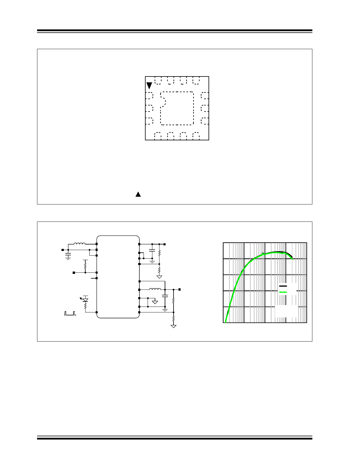
Package Type
Typical Application Schematic
SW1
OUT1
SW2
PGND2
PGND1
V
IN
FB1
NC
PG
EN
LED
OUT2
FB2
AGND
1
2
3
4
5
6
7
8
9
10
11
12
13
14
EP
14-Pin 2.5 mm x 2.5 mm QFN (FT)
(Top View)
Note:
Thin QFN Pin 1 identifier = “ ”.
50
60
70
80
90
100
0.0001
0.001
0.01
0.1
1
OUTPUT CURRENT (A)
25
°C
85
°C
V
IN
= 1.25V
V
OUT1
= 1.8V
6.8 μH
(0.9V-1.5V)
10 μF
V
OUT1
100k
PG
ON (V
IN
1.2V)
BLINKING (V
IN
< 1.2V)
0.25 Hz/25% DC
82
14
2
6
5
4
7
SW1
V
IN
EN
PG
NC
LED
OUT1
EP
PGND1
FB1
OUT2
SW2
AGND
PGND2
FB2
V
OUT1
13
1
3
10
12
8
11
9
47 μF
4.7 μH
10 μF
V
OUT1
1.8V/111 mA
V
OUT2
1.0V/30 mA
R3
R4
R1
R2
MIC23099
Efficiency (V
IN
= 1.25V)
vs. Output Current
E
F
F
ICI
E
NCY
(
%
)
2016 Microchip Technology Inc.
DS20005684A-page 3
MIC23099
Functional Block Diagram
6.8 μH
MIC23099
FAULT
BLOCK
OUT1
OUT2
EN1
EN2
START-UP
AND
SOFT-START
I
OUT1
= 0A
V
OUT1
> V
IN
SW1
(0.9V-1.5V)
10 μF
V
IN
EN
EN1
PWM1
CONTROL1LD
HD
V
IN
SYNC
BOOST
DISCHARGE
PFM MODE
S
R
Q
CLK
ON
NC
SLOPE
COMP
PWM
I
SNS1
I
SNS1
OUT1
47 μF
PGND1
FB1
R1
R2
V
OUT1
1.8V/111 mA
g
m
EA
V
REF
(0.6V)
PGOOD1
92.5% × V
REF
I
SNS2
EN2
PFM2
LD
HD
V
IN
SYNC
BUCK
DISCHARGE
S
R
Q
I
SNS2
80 mA
OSC
1 MHz
CLK
I
OUT2
= 0A
OUT2
4.7 μH
PGND2
FB2
R3
R4
V
OUT2
1.0V/30mA
SW2
10 μF
AGND
OVERTEMPERATURE
V
REF
(0.6V)
92.5% × V
REF
OT
150°C/130°C
PGOOD1
PGOOD2
LOW
BATT
V
IN
1.2V/1.215V
ON
t
RISE
DLY
V
OUT1
ON (V
IN
1.25V)
BLINKING (V
IN
< 1.2V)
0.25Hz/25% DC
82
LED
V
OUT1
100K
PG
PG
OT
4 M

MIC23099
DS20005684A-page 4
2016 Microchip Technology Inc.
1.0
ELECTRICAL CHARACTERISTICS
Absolute Maximum Ratings
†
Supply Voltage (V
IN
)................................................................................................................................... -0.3V to +6.0V
Switch Voltage (V
SW1
)................................................................................................................................ -0.3V to +6.0V
Switch Voltage (V
SW2
)................................................................................................................................ -0.8V to +6.0V
Enable Voltage (V
EN
) ..................................................................................................................................... -0.3V to V
IN
Feedback Voltage (V
FB
) ............................................................................................................................. -0.3V to +6.0V
LED Output (V
LED
) ..................................................................................................................................... -0.3V to +6.0V
Power Good (V
PG
) ..................................................................................................................................... -0.3V to +6.0V
AGND to PGND1, PGND2 ......................................................................................................................... -0.3V to +0.3V
Ambient Storage Temperature (T
S
) .........................................................................................................-65°C to +150°C
ESD HBM Rating
(
1
)
....................................................................................................................................................2 kV
ESD MM Rating.........................................................................................................................................................200V
Note 1:
Devices are ESD-sensitive. Handling precautions are recommended. Human body model, 1.5 k
in series
with 100 pF.
Operating Ratings
(
1
)
Input Voltage after Start-up (V
IN
) ........................................................................................................... +0.875V to +1.6V
Enable Voltage (V
EN
) ......................................................................................................................................... 0V to V
IN
LED Output (V
LED
) .........................................................................................................................................0V to V
OUT1
Output Voltage Range (V
OUT1
) ................................................................................................................. +1.8V to +3.3V
Output Voltage Range (V
OUT2
) ................................................................................................................ +1.0V to V
OUT1
Junction Temperature (T
J
)
(
2
)
...................................................................................................................-40°C to +125°C
Junction Thermal Resistance
2.5 mm x 2.5 mm Thin QFN-14 (
JA
) ............................................................................................................. +70°C/W
2.5 mm x 2.5 mm Thin QFN-14 (
JC
) ............................................................................................................. +25°C/W
Note 1:
The device is not ensured to function outside the operating range.
2:
The maximum allowable power dissipation is a function of the maximum junction temperature (T
J(MAX)
), the
junction-to-ambient thermal resistance (
JA
) and the ambient temperature (T
A
). The maximum allowable
power dissipation will result in excessive die temperature and the regulator will go into thermal shutdown.
†
Notice:
Stresses above those listed under “Maximum Ratings” may cause permanent damage to the device. This
is a stress rating only and functional operation of the device at those or any other conditions above those indi-
cated in the operational sections of this specification is not intended. Exposure to maximum rating conditions for
extended periods may affect device reliability.
2016 Microchip Technology Inc.
DS20005684A-page 5
MIC23099
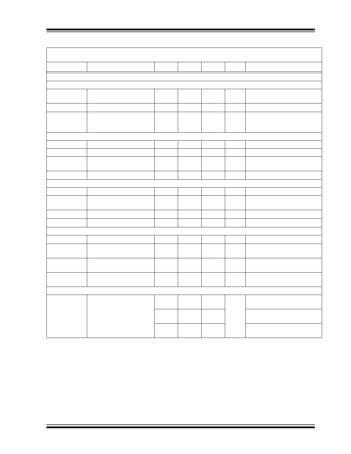
TABLE 1-1:
ELECTRICAL CHARACTERISTICS
(
1
)
Electrical Specifications:
unless otherwise specified, V
IN
= V
EN
= +1.25V; V
OUT1
= +1.8V; V
OUT2
= +1.0V; L
OUT1
= 6.8 µH;
L
OUT2
= 4.7 µH; C
OUT1
= 47 µF; C
OUT2
= 10 µF; T
A
= +25°C. Boldface values indicate -40°C
T
J
+125°C.
Symbol
Parameter
Min.
Typ.
Max.
Units
Test Conditions
Input Supply (V
IN
)
V
START(MIN)
Minimum Start-up Voltage
—
0.75
0.9
V
V
IN
rising, R
LOAD
500,
I
OUT2
= 0 mA
I
Q_PFM
Quiescent Current – PFM
Mode
—
200
270
µA
I
OUT1
, I
OUT2
= 0 mA (switching,
closed loop), measured at V
IN
with LED pin open
—
12.6
—
mA
I
OUT1
= 2 mA, I
OUT2
= 10 mA
(switching, closed loop),
measured at V
IN
I
SHDN
Shutdown Current
—
0.02
2
µA
V
EN
= 0V, V
IN
= 1.6V,
measured at V
IN
Enable Input (EN)
EN
HIGH
EN Logic Level High to
Start-up
0.8
0.58
—
V
V
EN
rising, regulator enabled
EN
LOW
EN Logic Level Low
—
0.5
0.2
V
V
EN
falling, regulator shutdown
I
ENBIAS
EN Bias Current
—
0.3
1
µA
V
EN
= 0V (regulator shutdown)
R
EN_PD
EN Pull-Down Resistance
3.0
4.0
5.0
M
I
EN
= 0.5 µA into pin
Solution Efficiency
System Efficiency
—
88
—
%
V
IN
= 1.25V, V
OUT1
= 1.8V,
V
OUT2
= 1.0V, P
OUT1
= 8 mW,
P
OUT2
= 20 mW
—
92
—
V
IN
= 1.25V, V
OUT1
= 1.8V,
V
OUT2
= 1.0V, P
OUT1
= 80 mW,
P
OUT2
= 20 mW
Note 1:
Specifications are for packaged product only.
2:
Ensured by design.
MIC23099
DS20005684A-page 6
2016 Microchip Technology Inc.
Fault Conditions
V
IN
and V
OUT1
, V
OUT2
Fault Conditions
V
VIN_OFF
V
IN
Turn-Off Threshold
Voltage
0.825
0.85
0.875
V
V
IN
falling, after start-up
V
PG_DLY(DEG)
PG Deglitch Delay, V
IN
Fault
120
—
180
ms
V
IN
falling below 0.85V to
V
PG
= Low
V
PG_DLY(DEG)
PG Deglitch Delay, V
OUT1
,
V
OUT2
Fault
60
—
120
ms
V
OUT1
or V
OUT2
falling below
90% of target value to
V
PG
= Low
T
COFF_DLY
Cool-Off Delay Time
750
1300
2250
ms
V
PG
= Low to V
OUT1
enabled,
C
OUT1
= 47 µF, C
OUT2
= 10 µF
Hiccup Cycles before
Latch-Off
—
15
—
Cycles Counts cool-off cycles
R
OUT1_DCHG
OUT1 Active Discharge
Resistance
—
500
700
V
EN
= 0V
R
OUT2_DCHG
OUT2 Active Discharge
Resistance
—
500
700
V
EN
= 0V
Power Good Output (PG)
V
PG_TH
PG Threshold Voltage
90
92.5
95
%V
REF1
V
REF1
rising or falling
90
92.5
95
%V
REF2
V
REF2
rising or falling
V
PG_LOW
PG Output Low Voltage
—
0.1
0.5
V
I
PG
= 1 mA (sinking), V
EN
= 0V
I
PG_LEAK
PG Leakage Current
-1
0.01
1
µA
V
PG
= 1.8V, V
EN
= 1.8V
t
PG_DLY
PG Turn-On Delay
10
—
50
ms
LED Low-Battery Indicator Output (LED)
V
LBVD
Low-Battery Threshold
1.15
1.2
1.25
V
V
IN
falling
L
B_HYST
Low-Battery Hysteresis
—
—
31
mV
V
IN
rising
f
LEDFLASH
LED Flash Frequency
0.125
0.25
0.5
Hz
V
IN
= 1.15V, V
EN
= 1.15V
D
LEDFLASH
LED Flash Duty Cycle
22.5
25
27.5
%
V
IN
= 1.15V, V
EN
= 1.15V
I
LK_LED
LED Output Leakage
Current
—
0.01
1
µA
V
LED
= 4.0V, V
EN
= 0V
R
LED(ON)
LED Switch-On Resistance
—
—
25
V
IN
= V
EN
= 1.25V,
I
LED
= 1.0 mA
Thermal Protection
T
SHD
Thermal Shutdown
—
150
—
°C
T
J
rising
T
SHD_HYST
Thermal Hysteresis
—
20
—
°C
Temperature decreasing
TABLE 1-1:
ELECTRICAL CHARACTERISTICS
(
1
)
(CONTINUED)
Electrical Specifications:
unless otherwise specified, V
IN
= V
EN
= +1.25V; V
OUT1
= +1.8V; V
OUT2
= +1.0V; L
OUT1
= 6.8 µH;
L
OUT2
= 4.7 µH; C
OUT1
= 47 µF; C
OUT2
= 10 µF; T
A
= +25°C. Boldface values indicate -40°C
T
J
+125°C.
Symbol
Parameter
Min.
Typ.
Max.
Units
Test Conditions
Note 1:
Specifications are for packaged product only.
2:
Ensured by design.
2016 Microchip Technology Inc.
DS20005684A-page 7
MIC23099
Boost
Boost Reference (FB1)
V
FB
Feedback Regulation
Voltage
0.579
0.6
0.621
V
V
IN
= 0.9V to 1.5V, PWM mode
I
FB_BIAS
FB Bias Current
—
1
500
nA
V
FB1
= 0.6V
T
SS_BOOST
Soft Start Time
—
5
—
ms
V
OUT1
: 10% to 90% of target
value, R
LOAD
= 500
;
C
OUT1
= 47 µF
Boost Internal MOSFETs
R
HS
High-Side On Resistance
—
200
—
m
I
SW1
= 100 mA, V
IN
= 1.25V
R
LS
Low-Side On Resistance
—
140
—
m
I
SW1
= 100 mA, V
IN
= 1.25V
I
SW1_LEAK
Leakage Current into SW1
—
0.01
2
µA
V
SW
= 4.0V, V
OUT1
= 0V,
V
EN
= 0V, V
IN
= 4.0V
R
AR_BOOST
Anti-Ringing Resistance
—
80
140
Boost Switching Frequency
f
SW
Switching Frequency
0.9
1.0
1.1
MHz
PWM mode
f
SW(MIN)_BOOST
Minimum Switching
Frequency
(
2
)
100
—
—
kHz
P
OUT1
= 20 mW (PFM mode)
D
MIN_BOOST
Minimum Duty Cycle
—
15
—
%
V
FB1
= 0.7V
D
MAX_BOOST
Maximum Duty Cycle
—
85
—
%
V
FB1
= 0.5V
Boost Current Limit
I
OUT(MAX)_BOOST
Maximum Output Power
—
450
—
mW
V
OUT1
> 1.8V, I
OUT2
= 0 mA
I
LIM_NMOS
Current-Limit Threshold
(NMOS)
1.0
1.5
2.0
A
V
FB1
= 0.5V
I
LIM_PMOS
Current-Limit Threshold
(PMOS)
1.5
2.5
3.0
A
V
FB1
= 0.5V
I
LIM_LINEAR(PMOS)
Linear Mode Current Limit
(PMOS)
56
80
180
mA
V
IN
= 1.25V, V
OUT1
= 0V
Boost Power Supply Rejection
PSRR (
V
IN
/
V
OUT1
)
—
50
—
dB
V
IN
= 200 mVp-p, f = 217 Hz,
I
OUT1
= PFM
—
50
—
V
IN
= 200 mVp-p, f = 1.0 kHz,
I
OUT1
= PFM
—
42
—
V
IN
= 200 mVp-p, f = 20 kHz,
I
OUT1
= PFM
TABLE 1-1:
ELECTRICAL CHARACTERISTICS
(
1
)
(CONTINUED)
Electrical Specifications:
unless otherwise specified, V
IN
= V
EN
= +1.25V; V
OUT1
= +1.8V; V
OUT2
= +1.0V; L
OUT1
= 6.8 µH;
L
OUT2
= 4.7 µH; C
OUT1
= 47 µF; C
OUT2
= 10 µF; T
A
= +25°C. Boldface values indicate -40°C
T
J
+125°C.
Symbol
Parameter
Min.
Typ.
Max.
Units
Test Conditions
Note 1:
Specifications are for packaged product only.
2:
Ensured by design.
MIC23099
DS20005684A-page 8
2016 Microchip Technology Inc.
Buck
Buck Reference (FB2)
V
FB2
Feedback Regulation
Voltage
0.579
0.6
0.621
V
V
OUT1
= 1.8V to 3.3V,
I
OUT2
= 6 mA to 30 mA (±3.5%)
I
FB2_BIAS
FB Bias Current
—
1
500
nA
V
FB2
=0.6V
t
SS
Soft Start Time
—
0.1
—
ms
V
OUT2
: 10% to 90% of target
value, I
OUT2
= 0 mA,
C
OUT2
= 10 µF
Buck Internal MOSFETs
R
HS_BUCK
High-Side On Resistance
—
560
—
m
I
SW2
= 100 mA, V
OUT1
= 1.8V
R
LS_BUCK
Low-Side On Resistance
—
380
—
m
I
SW2
= 100 mA, V
OUT1
= 1.8V
I
SW2LK_IN
Leakage Current into SW2
—
0.01
2
µA
V
OUT1
= 3.3V, V
SW2
= 3.3V,
V
EN
= 0V, V
OUT2
= 3.3V
I
SW2LK_OUT
Leakage Current out of SW2
—
0.01
0.5
µA
V
OUT1
= 3.3V, V
SW2
= 0V,
V
EN
= 0V, V
OUT2
= 0V
R
AR_BUCK
Anti-Ringing Resistance
—
80
140
W
Buck Switching Frequency
f
SW(MIN)_BUCK
Minimum Switching
Frequency
(
2
)
80
—
—
kHz
P
OUT2
= 8 mW (PFM mode)
D
MAX_BUCK
Maximum Duty Cycle
—
100
—
%
V
FB2
= 0.5V
Buck Current Limit
I
OUT(MAX)_BUCK
Maximum Output Current
—
30
—
mA
I
LIM_PMOS
Current-Limit Threshold
(PMOS)
—
80
120
mA
V
FB2
= 0.5V
Buck Power Supply Rejection
PSRR (
V
OUT1
/
V
OUT2
)
—
50
—
dB
V
OUT1
= 200 mVp-p,
f = 217 Hz, I
OUT2
= 10 mA
—
50
—
V
OUT1
= 200 mVp-p,
f = 1.0 kHz, I
OUT2
= 10 mA
—
42
—
V
OUT1
= 200 mVp-p,
f = 20 kHz, I
OUT2
= 10 mA
TABLE 1-1:
ELECTRICAL CHARACTERISTICS
(
1
)
(CONTINUED)
Electrical Specifications:
unless otherwise specified, V
IN
= V
EN
= +1.25V; V
OUT1
= +1.8V; V
OUT2
= +1.0V; L
OUT1
= 6.8 µH;
L
OUT2
= 4.7 µH; C
OUT1
= 47 µF; C
OUT2
= 10 µF; T
A
= +25°C. Boldface values indicate -40°C
T
J
+125°C.
Symbol
Parameter
Min.
Typ.
Max.
Units
Test Conditions
Note 1:
Specifications are for packaged product only.
2:
Ensured by design.
2016 Microchip Technology Inc.
DS20005684A-page 9
MIC23099
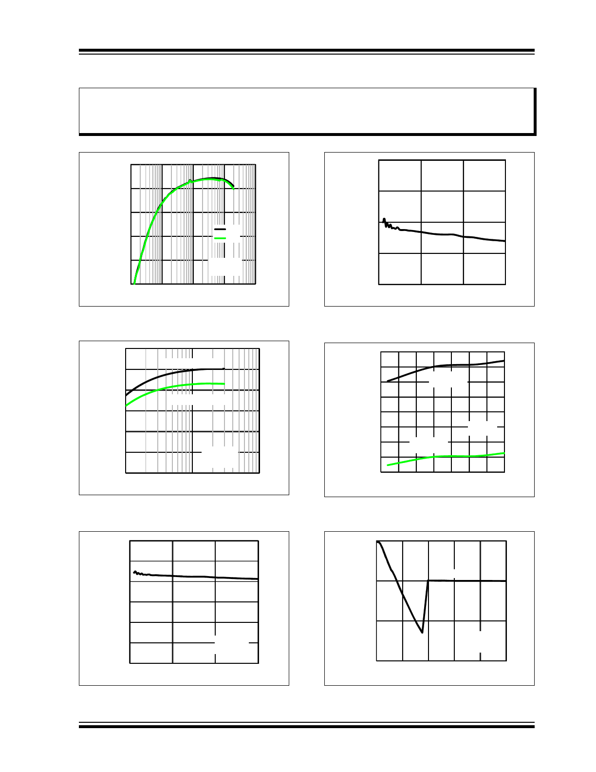
2.0
TYPICAL PERFORMANCE CURVES
FIGURE 2-1:
Efficiency (V
IN
= 1.25V) vs.
Output Current.
FIGURE 2-2:
Buck Efficiency (V
IN
= 1.8V)
vs. Output Current.
FIGURE 2-3:
Buck Output Voltage vs.
Output Current.
FIGURE 2-4:
Buck Load Regulation vs.
Output Current.
FIGURE 2-5:
Boost Feedback Voltage vs.
Temperature.
FIGURE 2-6:
Boost Output Voltage vs.
Output Current.
Note:
The graphs and tables provided following this note are a statistical summary based on a limited number of
samples and are provided for informational purposes only. The performance characteristics listed herein
are not tested or guaranteed. In some graphs or tables, the data presented may be outside the specified
operating range (e.g., outside specified power supply range) and therefore outside the warranted range.
50
60
70
80
90
100
0.0001
0.001
0.01
0.1
1
OUTPUT CURRENT (A)
25
°C
85
°C
V
IN
= 1.25V
V
OUT1
= 1.8V
E
F
F
ICI
E
NCY
(
%
)
40
50
60
70
80
90
100
0.001
0.01
0.1
OUTPUT CURRENT (A)
V
IN
= 1.8V
V
OUT2
= 1.0V
T
A
= 25°C
L2 = SPM4012T-4R7M
L2 = CIG2MW4R7NNE
E
F
F
ICI
E
NCY
(%)
0.97
0.98
0.99
1
1.01
1.02
1.03
0
0.01
0.02
0.03
OUTPUT CURRENT (A)
V
IN
= 1.8V
V
OUT2
= 1.0V
T
A
= 25°C
PFM
OUT
P
UT
V
O
L
T
AGE
(
V
)
-1.0%
-0.5%
0.0%
0.5%
1.0%
0
0.01
0.02
0.03
OUTPUT CURRENT (A)
V
IN
= 1.8V
V
OUT2
= 1.0V
T
A
= 25°C
PFM
L
O
AD RE
GUL
A
T
ION (
%
)
0.598
0.600
0.602
0.604
0.606
0.608
0.610
0.612
0.614
-50
-25
0
25
50
75
100
125
TEMPERATURE (
°C)
V
IN
= 1.2V
T
A
= 25°C
PFM
I
OUT1
= 100uA
PWM
I
OUT1
= 100mA
F
E
E
D
BACK V
O
L
T
AGE
(V
)
-4.0%
-2.0%
0.0%
2.0%
0
0.04
0.08
0.12
0.16
0.2
OUTPUT CURRENT (A)
V
IN
= 1.2V
V
OUT1
= 1.8V
T
A
= 25°C
PFM
PWM
LOA
D
R
E
GU
LA
TI
ON
(
%
)
MIC23099
DS20005684A-page 10
2016 Microchip Technology Inc.
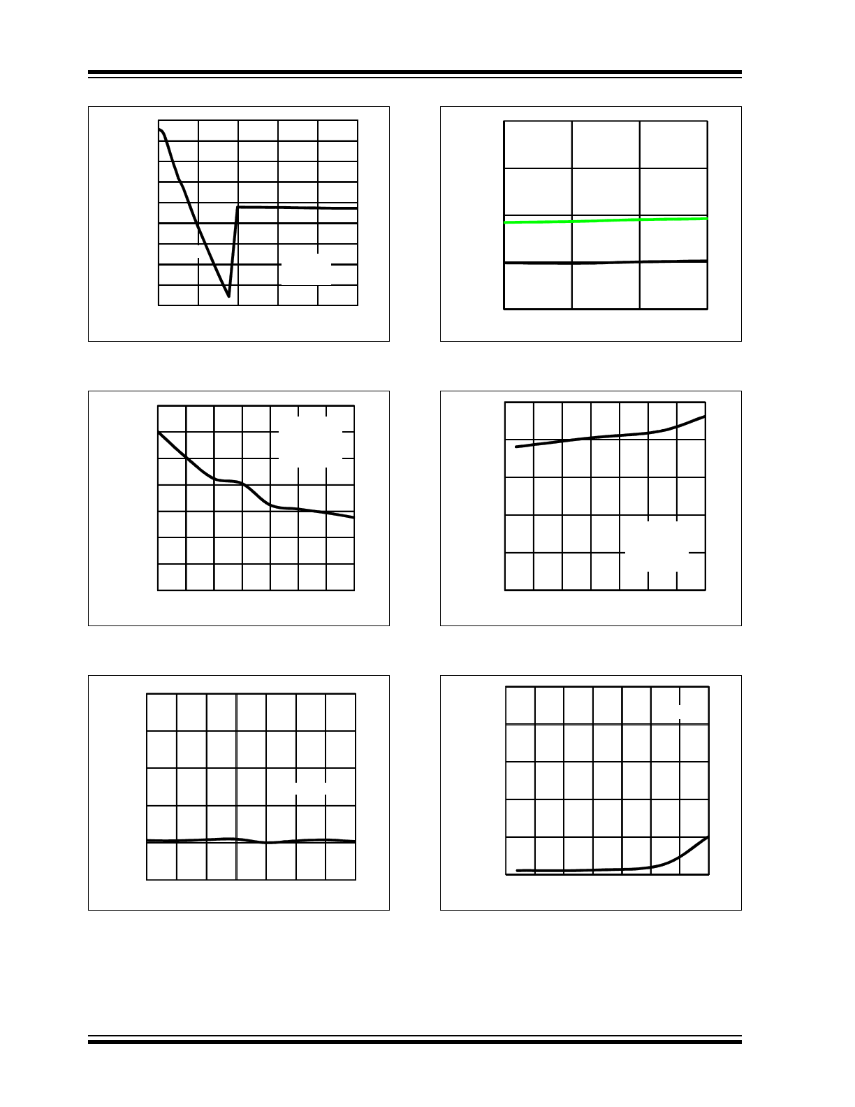
FIGURE 2-7:
Boost Output Voltage vs.
Output Current.
FIGURE 2-8:
V
IN
Quiescent Current
(Switching) vs. Input Voltage.
FIGURE 2-9:
V
IN
Shutdown Current vs.
Input Voltage.
FIGURE 2-10:
Enable Threshold vs. Input
Voltage.
FIGURE 2-11:
V
IN
Quiescent Current
(Switching) vs. Temperature.
FIGURE 2-12:
V
IN
Shutdown Supply
Current vs. Temperature.
1.75
1.76
1.77
1.78
1.79
1.80
1.81
1.82
1.83
1.84
0
0.04
0.08
0.12
0.16
0.2
OUTPUT CURRENT (A)
V
IN
= 1.2V
V
OUT1
= 1.8V
T
A
= 25°C
PWM
PFM
O
U
T
P
UT
V
O
L
T
AGE
(V
)
0
50
100
150
200
250
300
350
0.9
1.0
1.1
1.2
1.3
1.4
1.5
1.6
INPUT VOLTAGE (V)
I
OUT1
= 0A
I
OUT2
= 0A
LED = OPEN
SWITCHING
T
A
= 25°C
QUI
E
S
C
E
N
T
CURRE
NT
(µ
A)
0.0
0.1
0.2
0.3
0.4
0.5
0.9
1.0
1.1
1.2
1.3
1.4
1.5
1.6
INPUT VOLTAGE (V)
V
EN
= OPEN
S
HUT
DOW
N
CURRE
NT
(µ
A)
0.4
0.5
0.6
0.7
0.8
0.9
1.1
1.3
1.5
INPUT VOLTAGE(V)
Rising
Falling
T
A
= 25°C
EN
T
H
R
ESH
O
L
D
(V)
0
50
100
150
200
250
-50
-25
0
25
50
75
100
125
TEMPERATURE (
°C)
V
IN
= 1.2V
I
OUT1
= 0A
I
OUT2
= 0A
LED = OPEN
SWITCHING
QUI
E
S
C
E
N
T
CURRE
NT
(µ
A)
0.0
0.2
0.4
0.6
0.8
1.0
-50
-25
0
25
50
75
100
125
TEMPERATURE (
°C)
V
IN
= 1.2V
S
H
U
T
DOW
N
CURRE
NT
(µ
A)