
2017 Microchip Technology Inc.
DS20005748A-page 1
MIC2230
Features
• High Efficiency: Over 96%
• Ultra-Low Quiescent Current: Only 28 μA
• Ultra-Low Shutdown Current: Less Than 1 μA
• Fast Transient Performance
• 2.5 MHz PWM Operation
• High Output Current Capability per Channel:
800 mA
• No Schottky Diodes Required
• Stable with 2.2 μH Inductor, 10 μF Ceramic
Capacitor
• Adjustable Output Voltage Down to 0.8V
• Built-In Soft-Start Circuitry
• Current-Limit Protection
• Automatic Switching into Light Load Mode
Operation
• /FPWM Pin allows Low-Noise Forced PWM Mode
Operation
• Power Good Output with Internal 5 μA Current
Source allows Sequencing with Programmable
Delay Time
• Small Thermally Enhanced 3 mm × 3 mm
TDFN-12L Package
Applications
• MPU & ASIC Power
• PDAs
• Digital Cameras
• PC Cards
• Wireless and DSL Modems
General Description
The MIC2230 is a dual output, high-efficiency
synchronous step-down DC/DC converter. The
MIC2230 is ideally suited for portable and embedded
systems that demand high power conversion
efficiencies and fast transient performance, while
offered in a very small package. The MIC2230 offers an
ultra-low quiescent current in light load mode, assuring
minimum current draw from battery powered
applications in standby modes. The MIC2230 was
designed to only require miniature 2.2 μH inductors
and 10 μF ceramic capacitors.
The MIC2230 features a selectable mode that allows
the user to trade-off lowest noise performance for low
power efficiency. Trickle mode operation provides
ultra-high efficiency at light loads, while PWM operation
provides very low ripple noise performance. To
maximize battery life in low-dropout conditions,
MIC2230 can operate with a maximum duty cycle of
100%.
The MIC2230 is available in a space-saving
3 mm × 3 mm TDFN-12L package with a junction
temperature range from –40°C to +125°C.
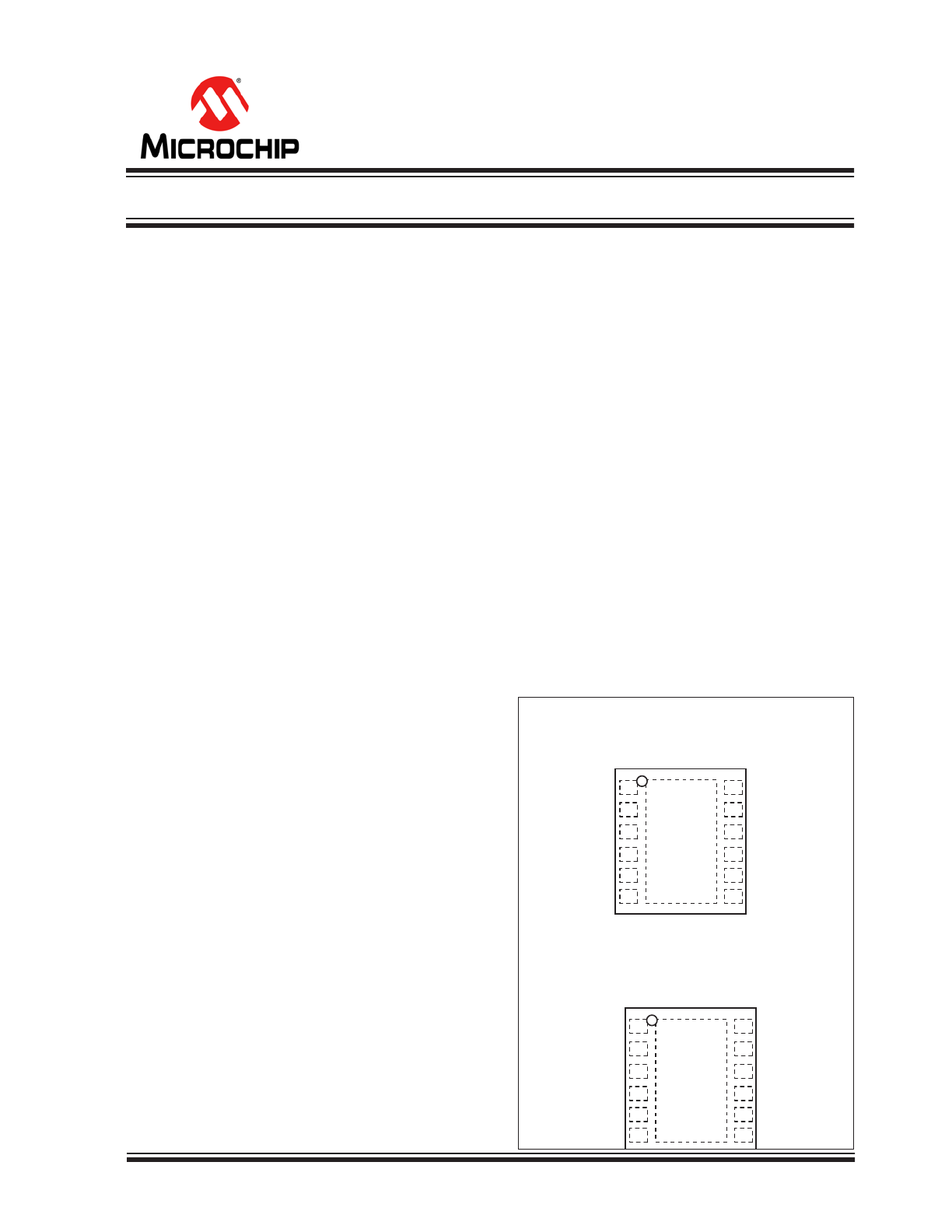
Package Types
MIC2230
3x3 TDFN* (Fixed)
Top View
AGND
SW1
5
1
OUT2
EN2
AVIN
SW2
12 OUT1
EN1
PGOOD
VIN
11
10
9
2
3
4
8
PGND
/FPWM
6
7
MIC2230
3x3 TDFN* (Adjustable)
Top View
AGND
SW1
5
1
FB2
EN2
AVIN
SW2
12 FB1
EN1
PGOOD
VIN
11
10
9
2
3
4
8
PGND
/FPWM
6
7
Dual Synchronous 800 mA/800 mA Step-Down DC/DC Regulator
MIC2230
DS20005748A-page 2
2017 Microchip Technology Inc.
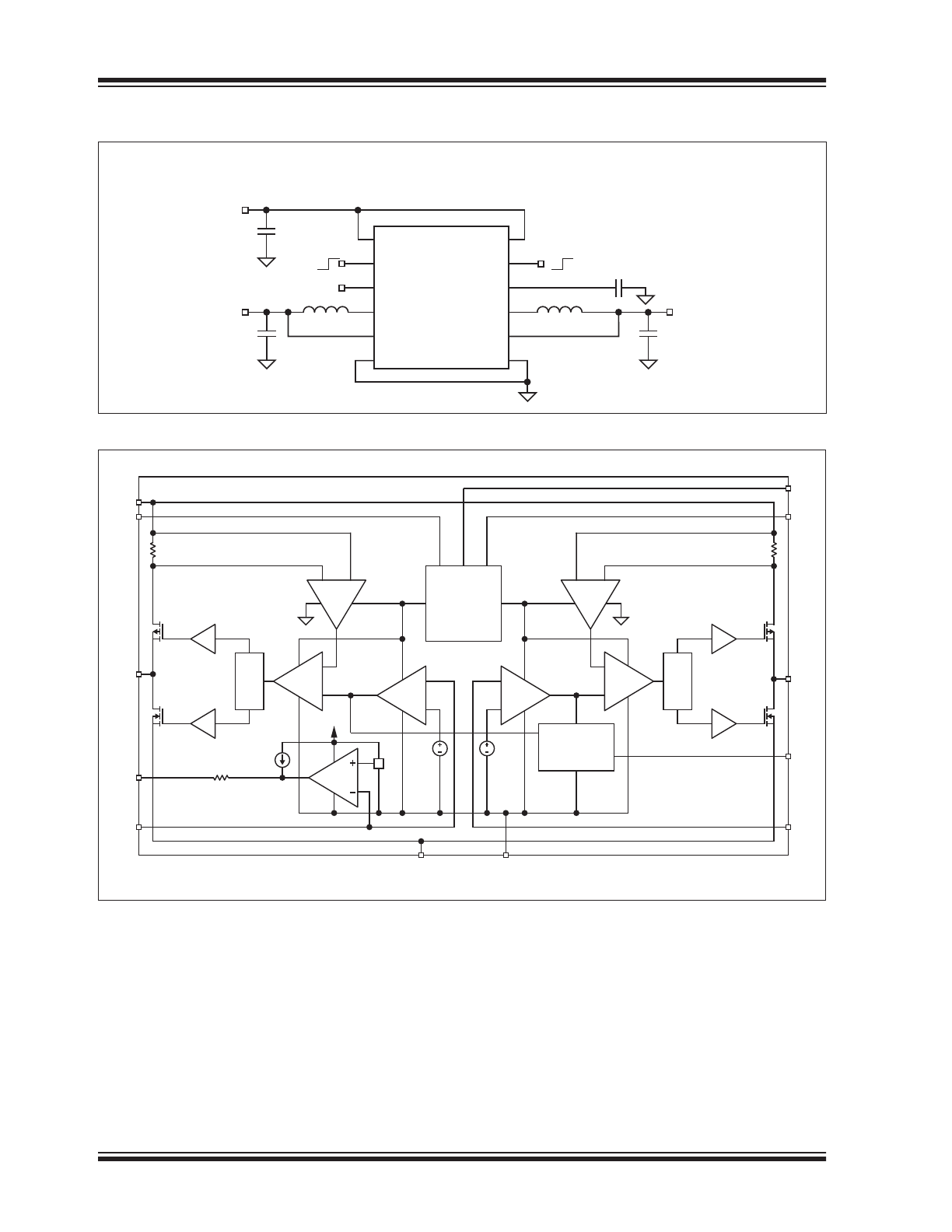
Typical Application Circuit
Functional Block Diagram
MIC2230
3x3 TDFN
EN2
SW2
PGND
OUT2
PGOOD
V
IN
2.5V to 5.5V
10μF
10μF
V
OUT
1
1.8V / 800mA
EN1
MIC2230
/FPWM
SW1
OUT1
2.2μH
VIN
AVIN
AGND
10μF
390pF
2.2μH
V
OUT
2
1.575V / 800mA
ON
OFF
ON
OFF
Compensation
Trickle Mode
Logic
Anti
Shoot-through
Logic
HSD
LSD
Anti
Shoot-through
Logic
HSD
LSD
ENABLE
LOGIC
VIN
EN1
SW1
PGOOD
FB1
PGND
AGND
FB2
/FPWM
SW2
EN2
AVIN
ISENSE2
ISENSE1
AVIN
EA1
EA2
5μA
0.8V
0.8V
1kΩ
2017 Microchip Technology Inc.
DS20005748A-page 3
MIC2230
1.0
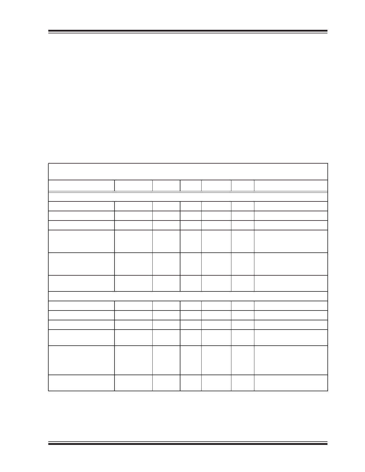
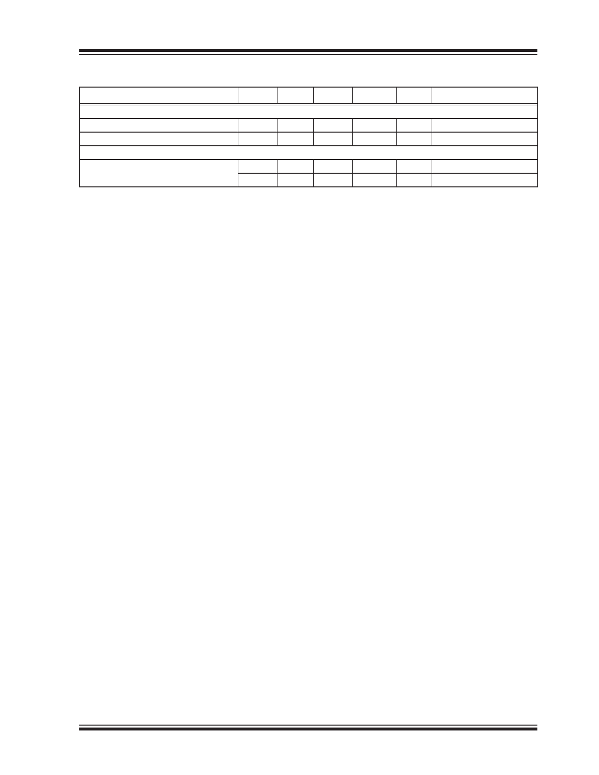
ELECTRICAL CHARACTERISTICS
Absolute Maximum Ratings †
Supply Voltage, (V
IN
) ................................................................................................................................................. +6V
Enable 1 Voltage ........................................................................................................................................................ +6V
Enable 2 Voltage ........................................................................................................................................................ +6V
Logic Input Voltage, (V
EN
, V
FPWM
)..................................................................................................................... 0V to V
IN
ESD Protection.........................................................................................................................................................+2 kV
Operating Ratings ††
Supply Voltage, V
IN
..................................................................................................................................... +2.5V to 5.5V
†
Notice: Exceeding the absolute maximum rating may damage the device.
††
Notice: The device is not guaranteed to function outside its operating rating.
DC CHARACTERISTICS (
Note 1
)
Electrical Characteristics:
Unless otherwise indicated, T
A
= 25°C with V
IN
= V
EN1
= V
EN2
= 3.6V, V
OUT1
, V
OUT2
:
L = 2.2 μH, C = 10 μF. Bold values indicate –40ºC
T
J
+125ºC.
Parameters
Sym.
Min.
Typ.
Max.
Units
Conditions
Supply Voltage and Current
Supply Voltage Range
2.5
—
5.5
V
—
UVLO (Rising)
2.3
2.4
2.5
V
—
UVLO Hysteresis
—
100
—
mV
—
PWM Mode Supply
Current
—
560
950
μA
/FPWM = Low; V
OUT1
,
V
OUT2
= 1.03 * V
NOM
(not
switching)
Trickle Mode Supply
Current
—
28
50
μA
/FPWM = High; V
OUT1
,
V
OUT2
= 1.03 * V
NOM
(not
switching)
Shutdown Quiescent
Current
—
0.1
1
μA
V
EN
= 0V
Output Voltage Accuracy
Feedback Voltage, V
FB
0.780
0.8
0.820
V
Adjustable
Output Voltage, V
OUT
–2.5
—
+2.5
%
Fixed Output Options
Feedback Bias Current
—
10
—
nA
—
Output Voltage Line
Regulation
—
0.1
0.5
%
2.5V
V
IN
5.5V
Output Voltage Load
Regulation
—
0.5
—
%
V
IN
= 5V, I
OUT
= 10 mA to
800 mA, /FPWM = 0V
V
IN
= 3V; I
OUT
= 10 mA to
800 mA, /FPWM = 0V
Ripple in Trickle Mode
—
40
—
mV
V
IN
=3.6V; I
OUT
= 1 mA;
C
OUT
= 10 μF, L = 2.2 μH.
Note 1:
Specification for packaged product only.
MIC2230
DS20005748A-page 4
2017 Microchip Technology Inc.
Logic Inputs
EN Input Threshold
—
0.8
1.2
V
On
0.3
0.7
—
V
Off
EN Input Current
—
0.01
1
μA
—
/FPWM Input Threshold
—
—
0.6×V
IN
V
On
0.3×V
IN
—
—
V
Off
/FPWM Input Current
—
0.01
1
μA
—
Protection
Current-Limit
0.9
1.2
1.8
A
—
Control
Maximum Duty Cycle
100
—
—
%
—
Oscillator
PWM Mode Frequency
2.125
2.5
2.875
MHz
—
Power Good
Power Good Reset
Threshold
—
6.25
12
%
Upper Threshold
–14
–8.5
—
%
Lower Threshold
PGOOD Series
Resistance
—
1
1.4
kΩ
—
PGOOD Pull-Up Current
—
5
—
μA
Output within 8.5% of
regulation
Power Switch
Switch On-Resistance
—
0.4
—
Ω
I
SW
= 150 mA (PFET)
—
0.35
—
Ω
I
SW
= 150 mA (NFET)
DC CHARACTERISTICS (
Note 1
) (CONTINUED)
Electrical Characteristics:
Unless otherwise indicated, T
A
= 25°C with V
IN
= V
EN1
= V
EN2
= 3.6V, V
OUT1
, V
OUT2
:
L = 2.2 μH, C = 10 μF. Bold values indicate –40ºC
T
J
+125ºC.
Parameters
Sym.
Min.
Typ.
Max.
Units
Conditions
Note 1:
Specification for packaged product only.
2017 Microchip Technology Inc.
DS20005748A-page 5
MIC2230
TEMPERATURE SPECIFICATIONS (
Note 1
)
Parameters
Sym.
Min.
Typ.
Max.
Units
Conditions
Temperature Ranges
Storage Temperature Range
T
A
–65
—
+150
°C
—
Junction Operating Temperature
T
J
–40
—
+125
°C
—
Package Thermal Resistances
Thermal Resistance, 3 x 3 QFN-12Ld
JA
—
60
—
°C/W
—
JC
—
15
—
°C/W
—
Note 1:
The maximum allowable power dissipation is a function of ambient temperature, the maximum allowable
junction temperature and the thermal resistance from junction to air (i.e., T
A
, T
J
,
JA
). Exceeding the
maximum allowable power dissipation will cause the device operating junction temperature to exceed the
maximum +125°C rating. Sustained junction temperatures above +125°C can impact the device reliability.
MIC2230
DS20005748A-page 6
2017 Microchip Technology Inc.
2.0
TYPICAL PERFORMANCE CURVES
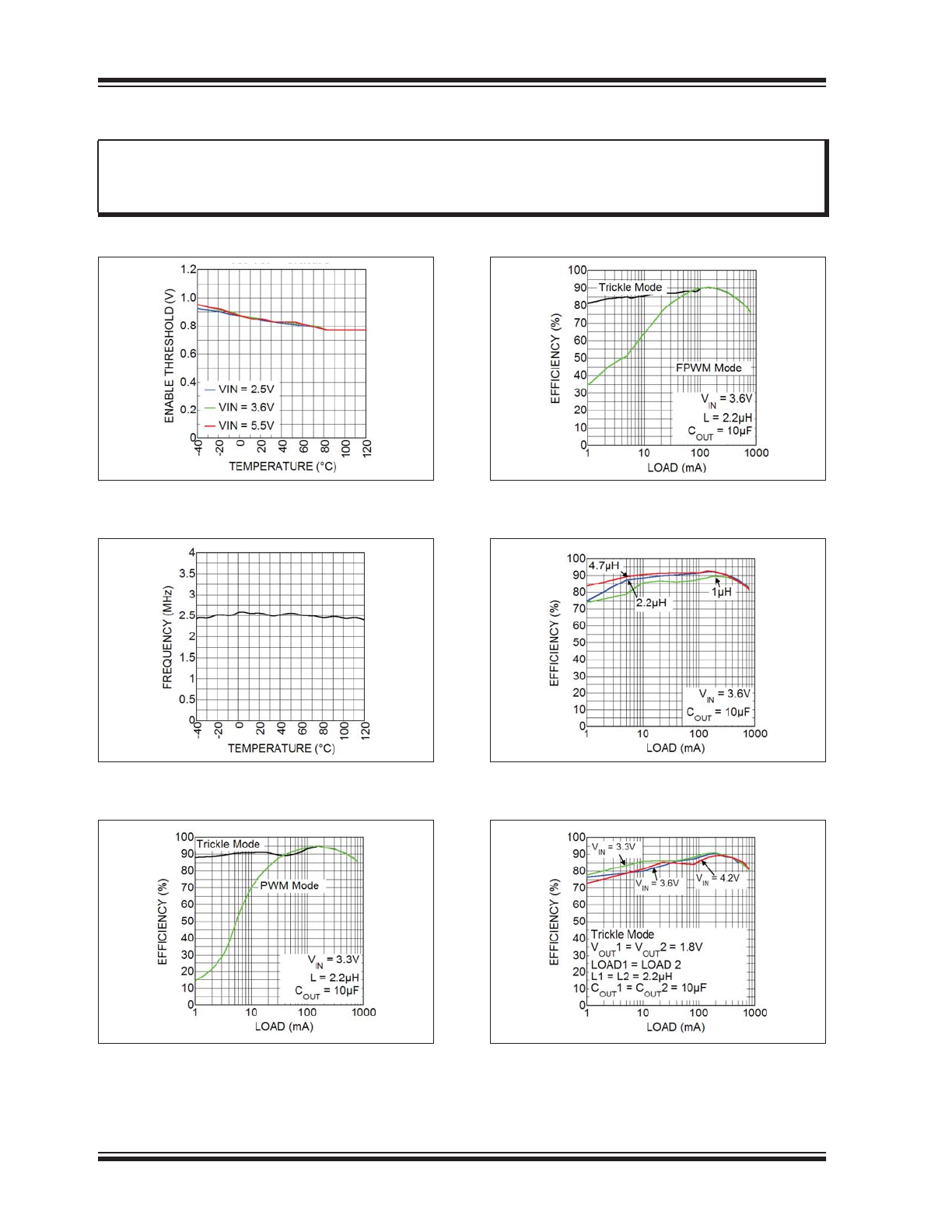
FIGURE 2-1:
Enabled Threshold vs.
Temperature.
FIGURE 2-2:
Frequency vs. Temperature.
FIGURE 2-3:
Efficiency.
FIGURE 2-4:
MIC2230 Efficiency
V
OUT
= 1.575V.
FIGURE 2-5:
MIC2230 Efficiency
V
OUT
= 1.8V.
FIGURE 2-6:
MIC2230 Efficiency
V
OUT1
= V
OUT2
= 1.8V.
Note:
The graphs and tables provided following this note are a statistical summary based on a limited number of
samples and are provided for informational purposes only. The performance characteristics listed herein
are not tested or guaranteed. In some graphs or tables, the data presented may be outside the specified
operating range (e.g., outside specified power supply range) and therefore outside the warranted range.
2017 Microchip Technology Inc.
DS20005748A-page 7
MIC2230
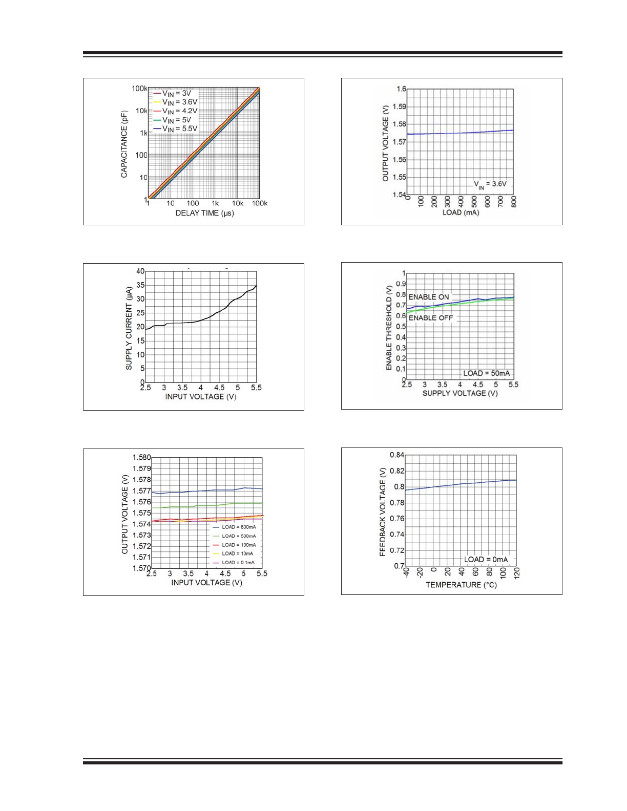
FIGURE 2-7:
Capacitance vs. Delay
Time.
FIGURE 2-8:
Trickle Mode Current vs.
Input Voltage.
FIGURE 2-9:
Output Voltage vs. Input
Voltage.
.
FIGURE 2-10:
Output Voltage vs. Load.
FIGURE 2-11:
Enable Threshold vs.
Supply Voltage.
FIGURE 2-12:
Feedback Voltage vs.
Temperature.
MIC2230
DS20005748A-page 8
2017 Microchip Technology Inc.
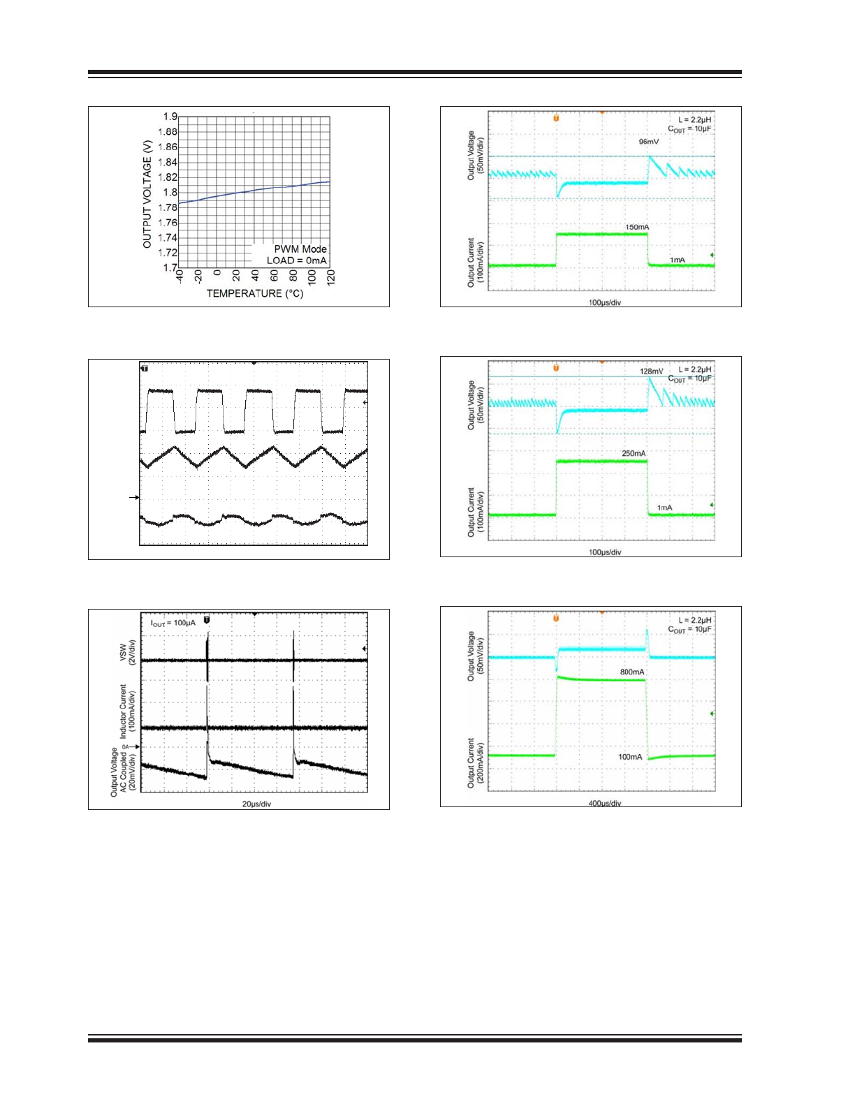
FIGURE 2-13:
Output Voltage vs.
Temperature.
FIGURE 2-14:
FPWM Mode.
FIGURE 2-15:
Trickle Mode.
FIGURE 2-16:
Load Transient Trickle
Mode.
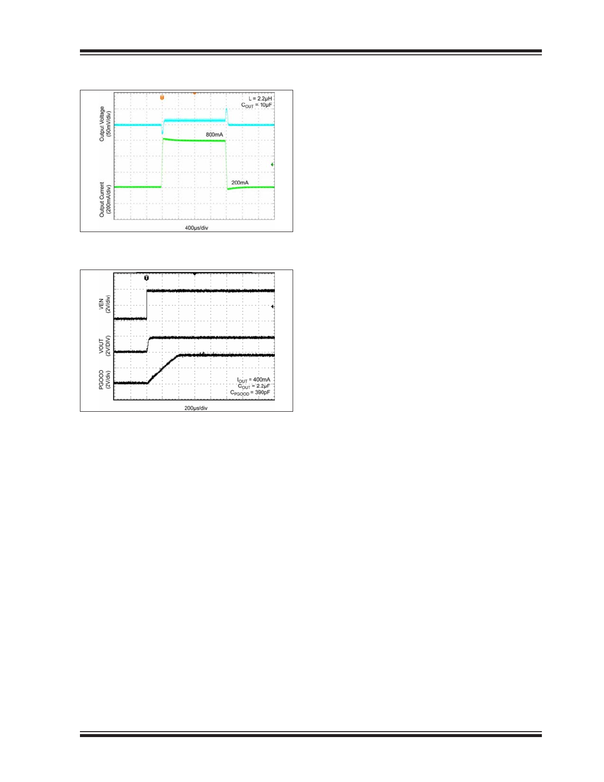
FIGURE 2-17:
Load Transient Trickle
Mode.
FIGURE 2-18:
Load Transient PWM Mode
.
VSW
(2V/div)
Output V
oltage
AC Coupled
(20mV/div)
Inductor Current
(200mA/div)
0A
200ns/div
V
IN
= 3.6V
V
OUT
= 1.8V
L = 2.2μH
/FPWM = 0
I
OUT
= 400mA
2017 Microchip Technology Inc.
DS20005748A-page 9
MIC2230
FIGURE 2-19:
Load Transient PWM Mode.
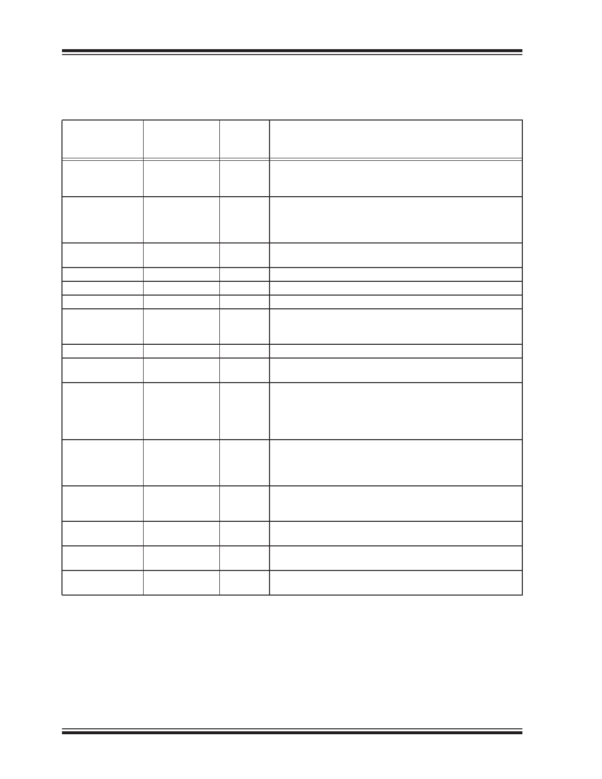
FIGURE 2-20:
Enable Response.
MIC2230
DS20005748A-page 10
2017 Microchip Technology Inc.
3.0
PIN DESCRIPTIONS
The descriptions of the pins are listed in
Table 3-1
.
TABLE 3-1:
PIN FUNCTION TABLE
MIC2230
Adjustable
3X3 QFN
MIC2230
Fixed
3X3 QFN
Symbol
Description
1
—
FB2
Feedback 2: For adjustable voltage options connect the exter-
nal resistor divider network to FB2 to set the output voltage of
regulator 2. Nominal value is 0.8V.
2
2
EN2
Enable 2 input. Logic low powers down regulator 2. Logic high
powers up regulator 2. MIC2230 features built-in soft-start
circuitry that reduces in-rush current and prevents the output
voltage from overshooting at start up.
3
3
AVIN
Analog Supply Voltage: Supply voltage for the analog control
circuitry. Requires bypass capacitor to GND.
4
4
SW2
Switch node for regulator 2, connected to external inductor.
5
5
AGND
Analog (signal) ground.
6
6
PGND
Power ground.
7
7
/FPWM
Forced PWM Mode Bar. Grounding this pin forces the device to
stay in constant frequency PWM mode only. Pulling this pin
high enables automatic Trickle Mode operation.
8
8
SW1
Switch node for regulator 1, connected to external inductor.
9
9
VIN
Supply Voltage: Supply voltage for the internal switches and
drivers. Requires bypass capacitor to GND.
10
10
PGOOD
Power Good Output. This output is pulled down unless the
regulator 1 output voltage is within +6.25% and –8.5% of
regulation. After the output voltage is in regulation, the output
starts to go high with an internal 5 μA current source. A delay
time could be programmed by tying a capacitor to this pin.
11
11
EN1
Enable 1 input. Logic low powers down regulator 1. Logic high
powers up regulator 1. MIC2230 features built-in soft-start
circuitry that reduces in-rush current and prevents the output
voltage from overshooting at start up.
12
–
FB1
Feedback 1: For adjustable voltage options connect to the
external resistor divider network to FB1 to set the output
voltage of regulator 1. Nominal value is 0.8V.
–
1
OUT2
Output Voltage 2. For fixed output voltage options connect
OUT2 to the output voltage of regulator 2.
–
12
OUT1
Output Voltage 1. For fixed output voltage options connect
OUT1 to the output voltage of regulator 1.
EP
EP
EP
Exposed Thermal pad. Should be connected to the Ground
plane.