
© 2009 Microchip Technology Inc.
DS22153C-page 1
MCP9843/98243
Features
• Meets JEDEC Specification
- MCP9843 - JC42.4-TSE3000B3
Temperature Sensor
- MCP98243 --> JC42.4-TSE2002B3
Temperature Sensor with 2 Kbit Serial
EEPROM for Serial Presence Detect (SPD)
• 2-wire I
2
C™/SMBus Interface
• Available Packages:
- DFN-8, TDFN-8, UDFN-8, TSSOP-8
Temperature Sensor Features
• Temperature-to-Digital Converter
• Sensor Accuracy (Grade B):
- ±0.2°C/±1°C (typ./max.)
→
+75°C to +95°C
- ±0.5°C/±2°C (typ./max.)
→
+40°C to +125°C
- ±1°C/±3°C (typ./max.)
→
-20°C to +125°C
• Specified V
DD
Range: 3.0V to 3.6V
• Operating Current: 200 µA (typical)
• Operating V
DD
Range: 2.7V to 5.5V
Serial EEPROM Features (MCP98243)
• Specified V
DD
Range: 1.8V to 5.5V
• Operating Current:
- Write
→ 1.1 mA (typical) for 3.5 ms (typical)
- Read
→ 100 µA (typical)
• Permanent and Reversible Software Write Protect
• Software Write Protection for the lower 1 Kbit
• Organized as 1 block of 256 x 8-bit (2 Kbit)
Typical Applications
• DIMM Modules for Servers, PCs, and Laptops
• General Purpose Temperature Datalog
Description
Microchip Technology Inc.’s MCP9843/98243 digital
temperature sensors convert temperature from -40°C
and +125°C to a digital word. These sensors meet
JEDEC Specification JC42.4-TSE3000B3 and
JC42.4-TSE2002B3 Memory Module Thermal Sensor
Component. It provides an accuracy of ±0.2°C/±1°C
(typical/maximum) from +75°C to +95°C. In addition,
MCP98243 has an internal 256 Byte EEPROM which
can be used to store memory module and vendor
information.
The MCP9843/98243 digital temperature sensor
comes with user-programmable registers that provide
flexibility for DIMM temperature-sensing applications.
The registers allow user-selectable settings such as
Shutdown or Low-Power modes and the specification
of temperature Event boundaries. When the
temperature changes beyond the specified Event
boundary limits, the MCP9843/98243 outputs an Alert
signal at the Event pin. The user has the option of
setting the temperature Event output signal polarity as
either an active-low or active-high comparator output
for thermostat operation, or as a temperature Event
interrupt output for microprocessor-based systems.
The MCP98243 EEPROM is designed specifically for
DRAM DIMMs (Dual In-line Memory Modules) Serial
Presence Detect (SPD). The lower 128 Bytes (address
0x00 to 0x7F) can be Permanent Write Protected
(PWP) or Software Reversible Write Protected (SWP).
This allows DRAM vendor and product information to
be stored and write protected. The upper 128 bytes
(address 0x80 to 0xFF) can be used for general
purpose data storage. These addresses are not write
protected.
This sensor has an industry standard 2-wire,
I
2
C compatible serial interface, allowing up to eight
devices to be controlled in a single serial bus.
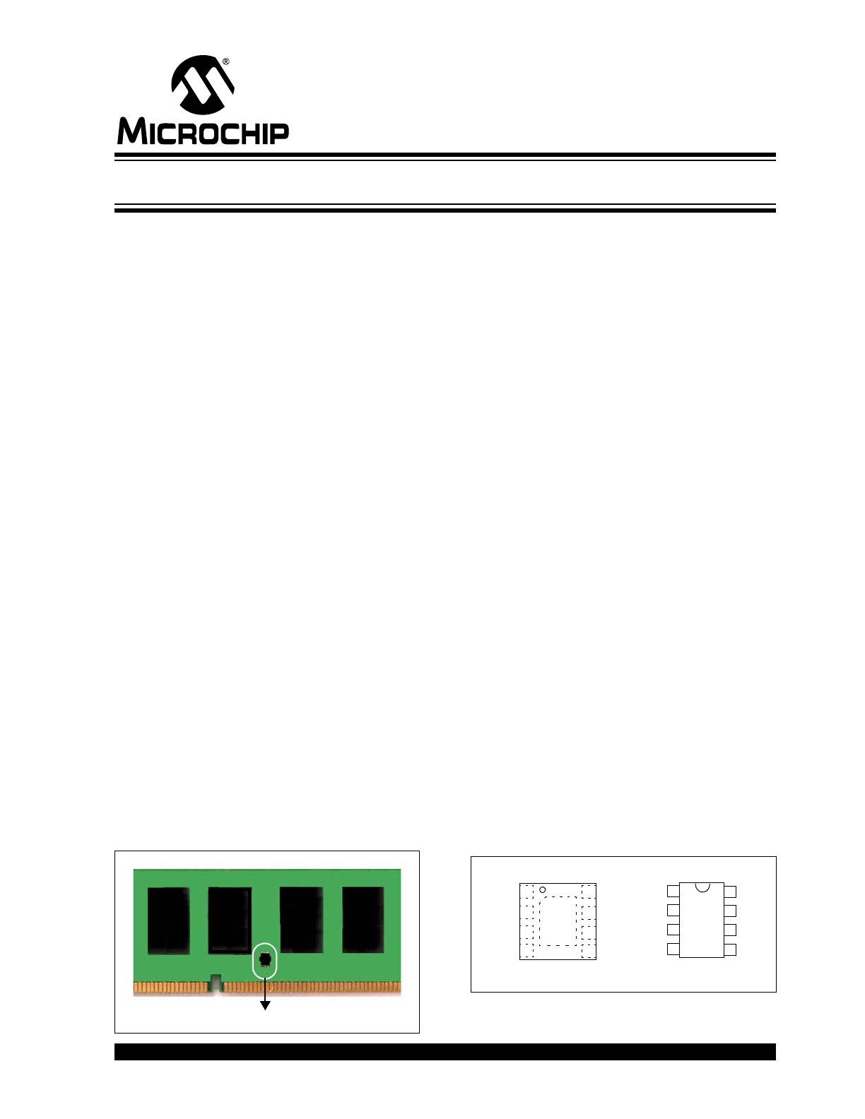
Package Types
DIMM MODULE
MCP9843/98243
8-Pin 2x3 DFN/TDFN/UDFN *
SDA
GND
Event
SCL
1
2
3
4
8-Pin TSSOP
A0
V
DD
A1
A2
8
7
6
5
* Includes Exposed Thermal Pad (EP); see
Table 3-1
.
SCL
Event
SDA
A1
A2
1
2
3
4
8
7
6
5
GND
A0
V
DD
EP
9
Memory Module Temperature Sensor w/ EEPROM for SPD
MCP9843/98243
DS22153C-page 2
© 2009 Microchip Technology Inc.
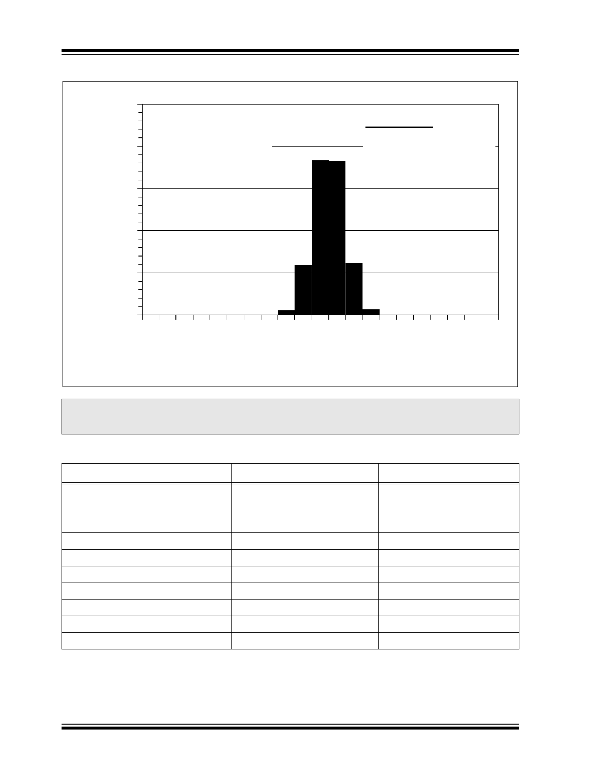
Sensor Typical Accuracy Performance
Note:
This accuracy data from the production system represents the typical accuracy performance of the
MCP98242 Memory Module Temperature Sensor. The MCP98242 production methodology is also used for
the MCP9843/98243 to achieve the same typical accuracy performance.
0%
10%
20%
30%
40%
50%
-1
.0
-0
.8
-0
.6
-0
.4
-0
.2
0.0
0.2
0.4
0.6
0.
8
1.0
Temperature Accuracy (°C)
O
ccu
rr
en
ces
T
A
= +85°C
1,063,478 units
63 Production lots
Statistics:
Average = 0.003 °C
St. Dev = 0.13 °C
±3 Sigma = ±0.4 °C
MCP98243 VS. MCP98242
Feature
MCP98243
MCP98242
Event Output in Shutdown Mode
Event Output De-asserts
Event Output Remains in previous
state. If the output asserts before
shutdown command, it remains
asserted during shutdown
I
2
C communication Timeout Range
t
OUT
= 25 ms to 35 ms
t
OUT
= 20 ms to 50 ms
I
2
C Maximum Bus Frequency
400 kHz
100 kHz
I
2
C SCL & SDA V
IL
/V
IH
voltage levels
V
IL_MAX
=0.3*V
DD
, V
IH_MIN
=0.7*V
DD
V
IL_MAX
= 0.8V, V
IH_MIN
= 2.1V
V
HV A0
range
7V to 12V
8V to 12V
I
2
C Spike Supression
50 ns
—
I
2
C input hysteresis
0.05V
DD
0.5V
Device/Revision ID Register
0x2101 (hex)
0x2001
© 2009 Microchip Technology Inc.
DS22153C-page 3
MCP9843/98243
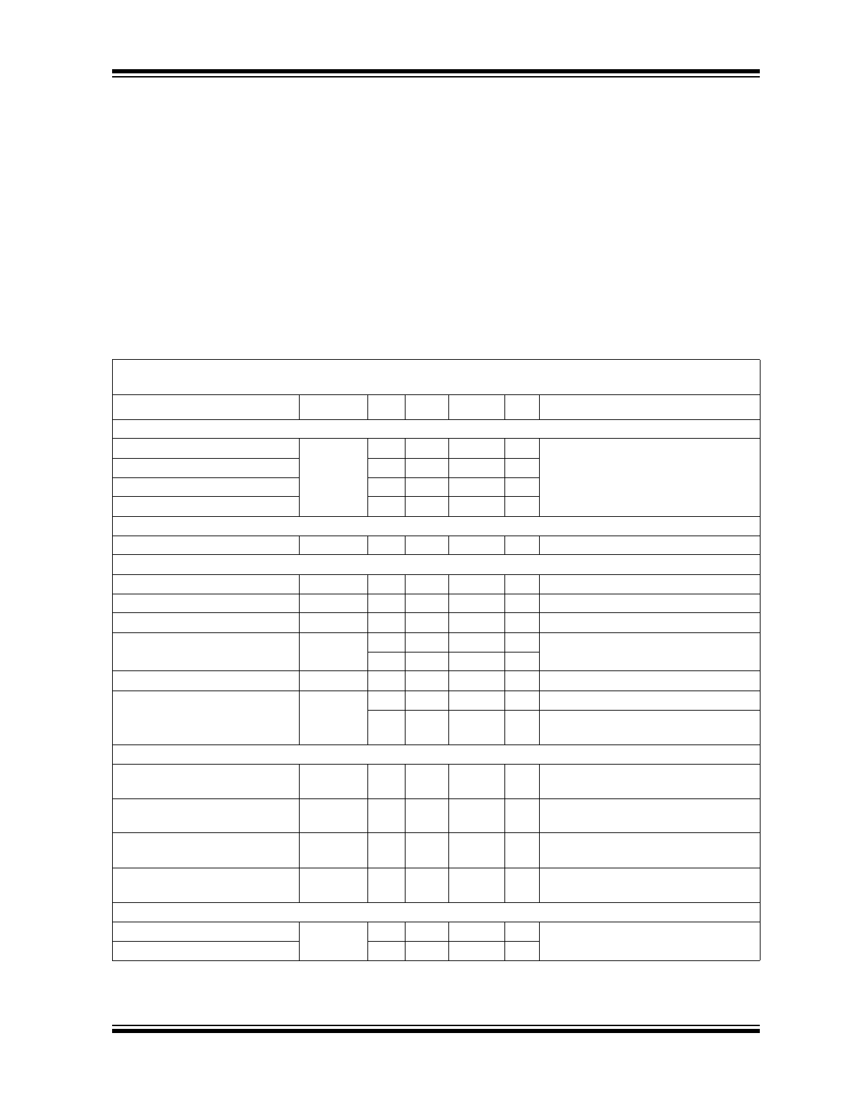
1.0
ELECTRICAL
CHARACTERISTICS
Absolute Maximum Ratings †
V
DD
.................................................................................. 6.0V
Voltage at all Input/Output pins ............... GND – 0.3V to 6.0V
Pin A0 ................................................... GND – 0.3V to 12.5V
Storage temperature .....................................-65°C to +150°C
Ambient temp. with power applied ................-40°C to +125°C
Junction Temperature (T
J
) .......................................... +150°C
ESD protection on all pins (HBM:MM) ................. (4 kV:300V)
Latch-Up Current at each pin (25°C) ....................... ±200 mA
†Notice: Stresses above those listed under “Maximum
ratings” may cause permanent damage to the device. This is
a stress rating only and functional operation of the device at
those or any other conditions above those indicated in the
operational listings of this specification is not implied.
Exposure to maximum rating conditions for extended periods
may affect device reliability.
TEMPERATURE SENSOR DC CHARACTERISTICS
Electrical Specifications: Unless otherwise indicated, V
DD
= 3.0V to 3.6V, GND = Ground,
and T
A
= -20°C to +125°C.
Parameters
Sym
Min
Typ
Max
Unit
Conditions
Temperature Sensor Accuracy
+75°C < T
A
≤ +95°C
T
ACY
-1.0
±0.2
+1.0
°C
JC42.4 - TSE2002B3
Grade B Accuracy Specification
+40°C < T
A
≤ +125°C
-2.0
±0.5
+2.0
°C
-20°C < T
A
≤ +125°C
-3.0
±1
+3.0
°C
T
A
= -40°C
—
-1
—
°C
Temperature Conversion Time
0.25°C/bit
t
CONV
—
65
125
ms 15 s/sec (typical) (See Section 5.2.4)
Power Supply
Specified Voltage Range
V
DD
3.0
—
3.6
V
JC42.4 Specified Voltage Range
Operating Voltage Range
V
DD
2.7
—
5.5
V
Note 1
Operating Current
I
DD_TS
—
200
500
µA
EEPROM Inactive
Shutdown Current - MCP9843
MCP98243
I
SHDN
—
1
2
µA
EEPROM Inactive, I
2
C Bus Inactive
—
1
3
µA
Power On Reset (POR)
V
POR_TS
—
2.2
—
V
Threshold for falling V
DD
voltage
Power Supply Rejection,
T
A
= +25°C
Δ°C/ΔV
DD
—
±0.3
—
°C/V V
DD
= 2.7V to 5.5V
—
±0.15
—
°C
V
DD
= 3.3V+150 mV
PP AC
(0 to 1 MHz)
Event Output (Open-Drain output, external pull-up or pull-down resistor required), see Section 5.2.3
High-level Current (leakage)
I
OH
—
—
1
µA
V
OH
= V
DD
(Active-Low, Pull-up
Resistor)
Low-level Voltage
V
OL
—
—
0.4
V
I
OL
= 3 mA (Active-Low, Pull-up
Resistor)
Low-level Current (leakage)
I
OL
—
—
1
µA
V
OL
= V
SS
(Active-High, Pull-down
Resistor)
High-level Voltage
V
OH
—
—
V
DD
-0.5
V
I
OH
= 3 mA (Active-High, Pull-down
Resistor)
Thermal Response, from +25°C (Air) to +125°C (oil bath)
DFN/UDFN/TDFN-8
t
RES
—
0.7
—
s
Time to 63% (89°C)
TSSOP-8
—
1.4
—
s
Note 1: Characterized but not production tested. Also, see Section 2.0 “Typical Performance Curves”.
MCP9843/98243
DS22153C-page 4
© 2009 Microchip Technology Inc.
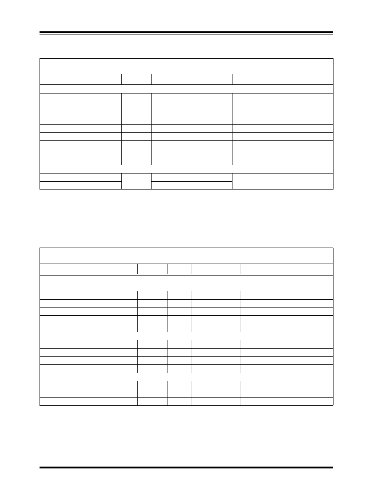
MCP98243 EEPROM DC CHARACTERISTICS
Electrical Specifications: Unless otherwise indicated, V
DD
= 1.8V to 5.5V, GND = Ground,
and T
A
= -20°C to +125°C.
Parameters
Sym
Min
Typ
Max
Unit
Conditions
Power Supply
Operating Voltage Range
V
DD
1.8
—
5.5
V
Current, EEPROM write
I
DD_EE
—
1100
2000
µA
Sensor in Shutdown Mode (for t
WC
),
(Note 1)
Current, EEPROM read
I
DD_EE
—
100
500
µA
Sensor in Shutdown Mode (Note 1)
Power On Reset (POR)
V
POR_EE
—
1.6
—
V
EEPROM
Write Cycle time (byte/page)
t
WC
—
3
5
ms
Endurance T
A
= +25°C
—
—
1M
—
cycles Number of Write Cycles, V
DD
= 5V (Note 2)
EEPROM Write Temperature
EE
WRITE
0
—
85
°C
EEPROM Read Temperature
EE
READ
-40
—
125
°C
For minimum read temperature, see Note 2
Write Protect Voltage
SWP and CWP Voltage
V
HV
7
—
12
V
Applied at A0 pin (Note 3)
PWP Voltage
—
V
DD
—
V
Note 1:
For V
DD
ranges of 1.8V to the temperature sensor V
POR_TS
, the temperature sensor becomes partially biased and
consumes 80 µA (typical) until the sensor POR resets and acknowledges a shutdown command. See
Figure 2-15
.
2:
Characterized but not production tested. For endurance estimates in a specific application, please consult the Total
Endurance™ Model which can be obtained from Microchip’s web site at www.microchip.com.
3:
The range of voltage applied at A0 pin for Permanent Write Protect is GND to V
DD
+ 1V. See
Figure 2-13
and
Section 5.3.3 “Write Protection”.
INPUT/OUTPUT PIN DC CHARACTERISTICS (NOTE 1)
Electrical Specifications: Unless otherwise indicated, V
DD
= 1.8V to 5.5V, GND = Ground and
T
A
= -20°C to +125°C.
Parameters
Sym
Min
Typ
Max
Units
Conditions
Serial Input/Output (SCL, SDA, A0, A1, A2) (Note 2)
Input
High-level Voltage
V
IH
0.7V
DD
—
—
V
Low-level Voltage
V
IL
—
—
0.3V
DD
V
Input Current
I
IN
—
—
±5
µA
SDA and SCL only
Input Impedance (A0, A1, A2)
Z
IN
—
1
—
M
Ω
V
IN
> V
IH
Input Impedance (A0, A1, A2)
Z
IN
—
200
—
k
Ω
V
IN
< V
IL
Output (SDA only)
Low-level Voltage
V
OL
—
—
0.4
V
I
OL
= 3 mA
High-level Current (leakage)
I
OH
—
—
1
µA
V
OH
= V
DD
Low-level Current
I
OL
6
—
—
mA
V
OL
= 0.6V
Capacitance
C
IN
—
5
—
pF
SDA and SCL Inputs
Hysteresis
V
HYST
—
0.05V
DD
—
V
V
DD
> 2V
—
0.1V
DD
—
V
V
DD
< 2V
Spike Supression
T
SP
—
—
50
ns
Note 1: These specifications apply for the Temperature Sensor and EEPROM.
2: For V
DD
ranges of 1.8V to the temperature sensor V
POR_TS
, the temperature sensor becomes partially
biased and consumes 80 µA (typical) until the sensor POR resets and acknowledges a shutdown
command. See
Figure 2-15
.

© 2009 Microchip Technology Inc.
DS22153C-page 5
MCP9843/98243
SENSOR AND EEPROM SERIAL INTERFACE TIMING SPECIFICATIONS
Electrical Specifications: Unless otherwise indicated, GND = Ground, T
A
= -20°C to +125°C, and C
L
= 80 pF
(Note 1, 5).
V
DD
= 1.8V to 5.5V V
DD
= 2.2V to 5.5V
Parameters
Sym
Min
Max
Min
Max
Units
Conditions
2-Wire I
2
C Interface
Serial port frequency
f
SCL
10
100
10
400
kHz
Note 2, 4
Low Clock
t
LOW
4700
—
1300
—
ns
Note 2
High Clock
t
HIGH
4000
—
600
—
ns
Note 2
Rise time
t
R
—
1000
20
300
ns
Fall time
t
F
20
300
20
300
ns
Data in Setup time
t
SU:DI
250
—
100
—
ns
Note 3
Data in Hold time
t
HD:DI
0
—
0
—
ns
Note 6
Data out Hold time
t
HD:DO
200
900
200
900
ns
Note 4
Start Condition Setup time
t
SU:STA
4700
—
600
—
ns
Start Condition Hold time
t
HD:STA
4000
—
600
—
ns
Stop Condition Setup time
t
SU:STO
4000
—
600
—
ns
Bus idle
t
B:FREE
4700
—
1300
—
ns
Time out (Sensor Only)
t
OUT
—
—
25
35
ms
V
DD
= 3.0V to 3.6V
Bus Capacitive load
C
b
—
—
—
400
pf
Note 1: All values referred to V
IL MAX
and V
IH MIN
levels.
2: If t
LOW
> t
OUT
or t
HIGH
> t
OUT
, the temperature sensor I
2
C interface will time out. A Repeat Start command
is required for communication.
3: This device can be used in a Standard-mode I
2
C-bus system, but the requirement t
SU:DAT
≥ 250 ns must
be met. This device does not stretch SCL Low time. It outputs the next data bit to the SDA line within
t
R MAX
+ t
SU:DI MIN
= 1000 ns + 250 ns = 1250 ns (according to the Standard-mode I
2
C-bus specification)
before the SCL line is released.
4: As a transmitter, the device provides internal minimum delay time t
HD:DAT MIN
to bridge the undefined
region (min. 300 ns) of the falling edge of SCL t
F MAX
to avoid unintended generation of Start or Stop
conditions.
5: For V
DD
ranges of 1.8V to the temperature sensor V
POR_TS
, the temperature sensor becomes partially
biased and consumes 100 µA (typical) until the sensor POR resets and acknowledges a shutdown com-
mand.
6: As a receiver, SDA should not be sampled at the falling edge of SCL. SDA can transition t
HD:DI
0 ns after
SCL toggles Low.
MCP9843/98243
DS22153C-page 6
© 2009 Microchip Technology Inc.
TEMPERATURE CHARACTERISTICS
TIMING DIAGRAM
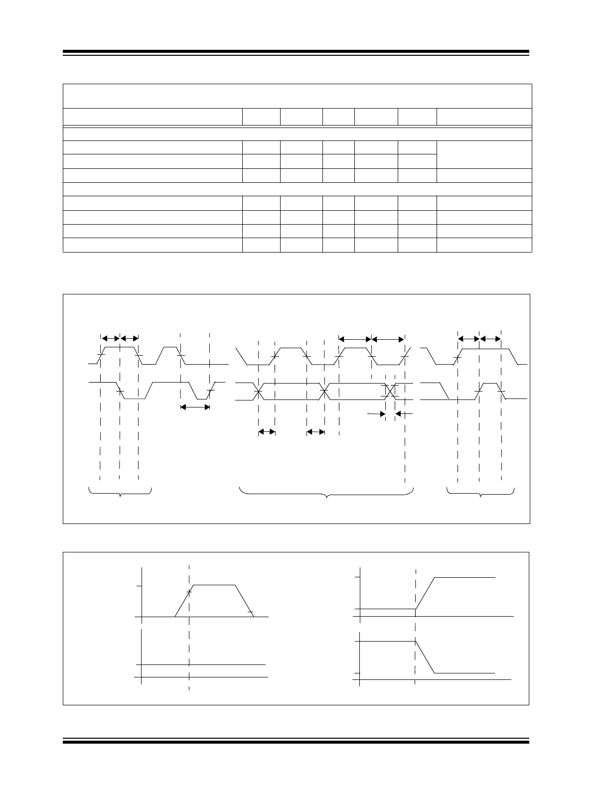
GRAPHICAL SYMBOL DESCRIPTION
Electrical Specifications: Unless otherwise indicated, V
DD
= 1.8V to 5.5V for the EEPROM, V
DD
= 3.0V to 3.6V for
the Temperature Sensor, and GND = Ground.
Parameters
Sym
Min
Typ
Max
Units
Conditions
Temperature Ranges
Specified Temperature Range
T
A
-20
—
+125
°C
Note 1
Operating Temperature Range
T
A
-40
—
+125
°C
Storage Temperature Range
T
A
-65
—
+150
°C
Thermal Package Resistances
Thermal Resistance, 8L-DFN
θ
JA
—
68
—
°C/W
Thermal Resistance, 8L-TDFN
θ
JA
—
52.5
—
°C/W
Thermal Resistance, 8L-TSSOP
θ
JA
—
139
—
°C/W
Thermal Resistance, 8L-UDFN
θ
JA
—
41
—
°C/W
Note 1: Operation in this range must not cause T
J
to exceed Maximum Junction Temperature (+150°C).
t
SU:
ST
O
t
SU
:D
I
t
SU:
DI
t
SU
:S
TO
t
B:
FR
EE
SC
L
SD
A
t
HD
:DI
/
t
HD:
DO
t
HIGH
t
LOW
t
OU
T
t
R
, t
F
Start Condition
Data Transmission
Stop Condition
V
DD
V
IH
V
IL
I
IN
Voltage
Current
time
V
DD
I
OH
Voltage
Current
time
INPUT
OUTPUT
V
OL
I
OL
© 2009 Microchip Technology Inc.
DS22153C-page 7
MCP9843/98243
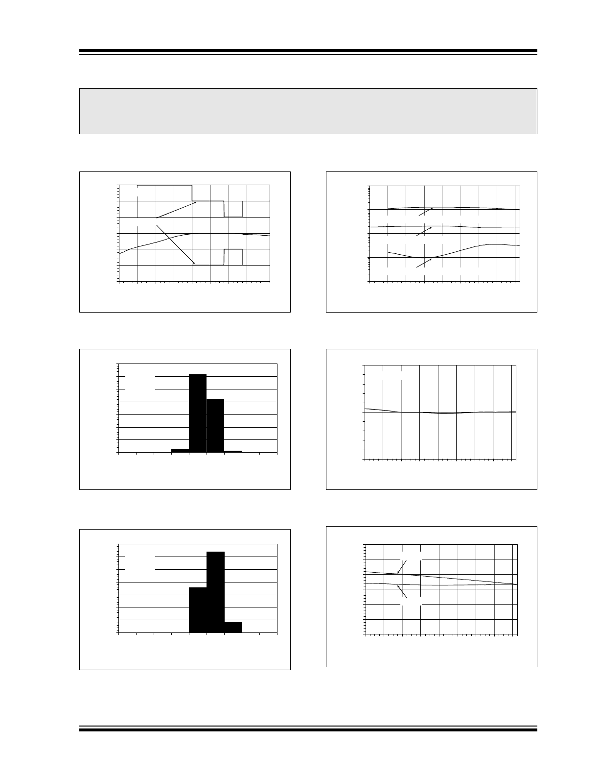
2.0
TYPICAL PERFORMANCE CURVES
Note: Unless otherwise indicated, V
DD
= 2.7V to 5.5V, GND = Ground, SDA/SCL pulled-up to V
DD
, and
T
A
= -40°C to +125°C.
FIGURE 2-1:
Average Temperature
Accuracy.
FIGURE 2-2:
Temperature Accuracy
Histogram, T
A
= +95°C.
FIGURE 2-3:
Temperature Accuracy
Histogram, T
A
= +75°C.
FIGURE 2-4:
Supply Current vs.
Temperature.
FIGURE 2-5:
Serial Bus Time-Out vs.
Temperature.
FIGURE 2-6:
Power-on Reset Threshold
Voltage vs. Temperature.
Note:
The graphs and tables provided following this note are a statistical summary based on a limited number of
samples and are provided for informational purposes only. The performance characteristics listed herein
are not tested or guaranteed. In some graphs or tables, the data presented may be outside the specified
operating range (e.g., outside specified power supply range) and therefore outside the warranted range.
-3.0
-2.0
-1.0
0.0
1.0
2.0
3.0
-40
-20
0
20
40
60
80
100 120
T
A
(°C)
T
e
mp
erat
u
re
A
ccu
racy
(
°C
)
V
DD
= 3.3V
Spec. Limits
0%
10%
20%
30%
40%
50%
60%
70%
-1.
0
0
-0.
7
5
-0.
5
0
-0.
2
5
0.00
0.25
0.50
0.75
1.00
Temperature Accuracy (°C)
O
ccu
rrenc
es
T
A
= +95°C
V
DD
= 3.3V
221 units
0%
10%
20%
30%
40%
50%
60%
70%
-1.
0
0
-0.
7
5
-0.
5
0
-0.
2
5
0.0
0
0.2
5
0.5
0
0.7
5
1.0
0
Temperature Accuracy (°C)
O
ccu
rr
enc
es
T
A
= +75°C
V
DD
= 3.3V
221 units
1
10
100
1000
10000
-40
-20
0
20
40
60
80
100 120
T
A
(°C)
I
DD
(µ
A
)
EEPROM Write (Sensor in Shutdown Mode)
Sensor (EEPROM Inactive)
EEPROM Read (Sensor in Shutdown Mode)
25
30
35
-40
-20
0
20
40
60
80
100 120
T
A
(°C)
t
OU
T
(m
s)
V
DD
= 3.3V to 3.6V
0
0.5
1
1.5
2
2.5
3
-40
-20
0
20
40
60
80
100 120
T
A
(°C)
V
PO
R
(V
)
V
POR_TS
V
POR_EE
MCP9843/98243
DS22153C-page 8
© 2009 Microchip Technology Inc.
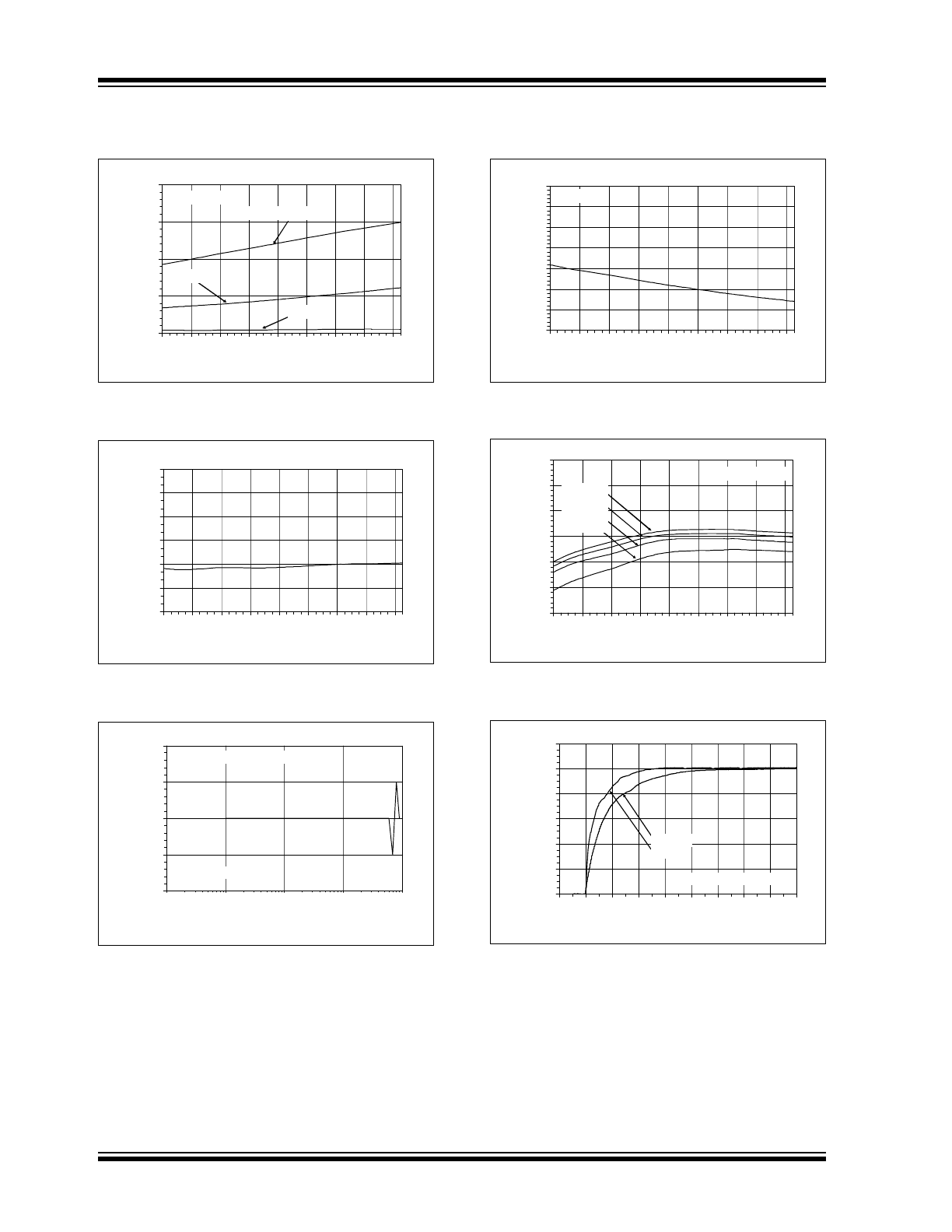
Note: Unless otherwise indicated, V
DD
= 2.7V to 5.5V, GND = Ground, SDA/SCL pulled-up to V
DD
, and
T
A
= -40°C to +125°C.
FIGURE 2-7:
Event and SDA V
OL
vs.
Temperature.
FIGURE 2-8:
Conversion Rate vs.
Temperature.
FIGURE 2-9:
Power Supply Rejection vs.
Frequency.
FIGURE 2-10:
SDA I
OL
vs. Temperature.
FIGURE 2-11:
Temperature Accuracy vs.
V
DD
.
FIGURE 2-12:
Package Thermal
Response.
0
0.1
0.2
0.3
0.4
-40
-20
0
20
40
60
80
100 120
T
A
(°C)
SD
A
a
n
d
Ev
en
t Ou
tp
u
t
(V
)
Event V
OL
SDA V
OL
I
OH
= I
OL
= 3 mA
Event (V
DD
- V
OH
)
35
50
65
80
95
110
125
-40
-20
0
20
40
60
80
100 120
T
A
(°C)
t
CO
NV
(m
s
)
-1.0
-0.5
0.0
0.5
1.0
100
1,000
10,000
100,000
1,000,000
Frequency (Hz)
N
o
rm
a
li
ze
d
T
e
mp
.
E
rro
r
(°
C
)
Δ°C/ΔV
DD
, V
DD
= 3.3V + 150 mV
PP (AC)
1k
10k
100k
1M
100k
1M
10k
100k
1M
1k
10k
100k
1M
100
1k
10k
100k
1M
T
A
= 25°C
No decoupling capacitor
6
12
18
24
30
36
42
48
-40
-20
0
20
40
60
80
100 120
T
A
(°C)
S
DA I
OL
(m
A)
V
OL
= 0.6V
-3.0
-2.0
-1.0
0.0
1.0
2.0
3.0
-40
-20
0
20
40
60
80
100 120
T
A
(°C)
T
em
p
er
at
u
re Ac
cu
ra
cy
(
°C
)
Δ°C/ΔV
DD
= 0.4°C/V
V
DD
= 2.7V
V
DD
= 3.0V
V
DD
= 3.6V
V
DD
= 5.5V
0%
20%
40%
60%
80%
100%
120%
-2
0
2
4
6
8
10
12
14
16
Time (s)
The
rm
al
R
espo
n
se
(%
)
22°C (Air) to 125°C (Oil bath)
TSSOP-8
DFN-8
© 2009 Microchip Technology Inc.
DS22153C-page 9
MCP9843/98243
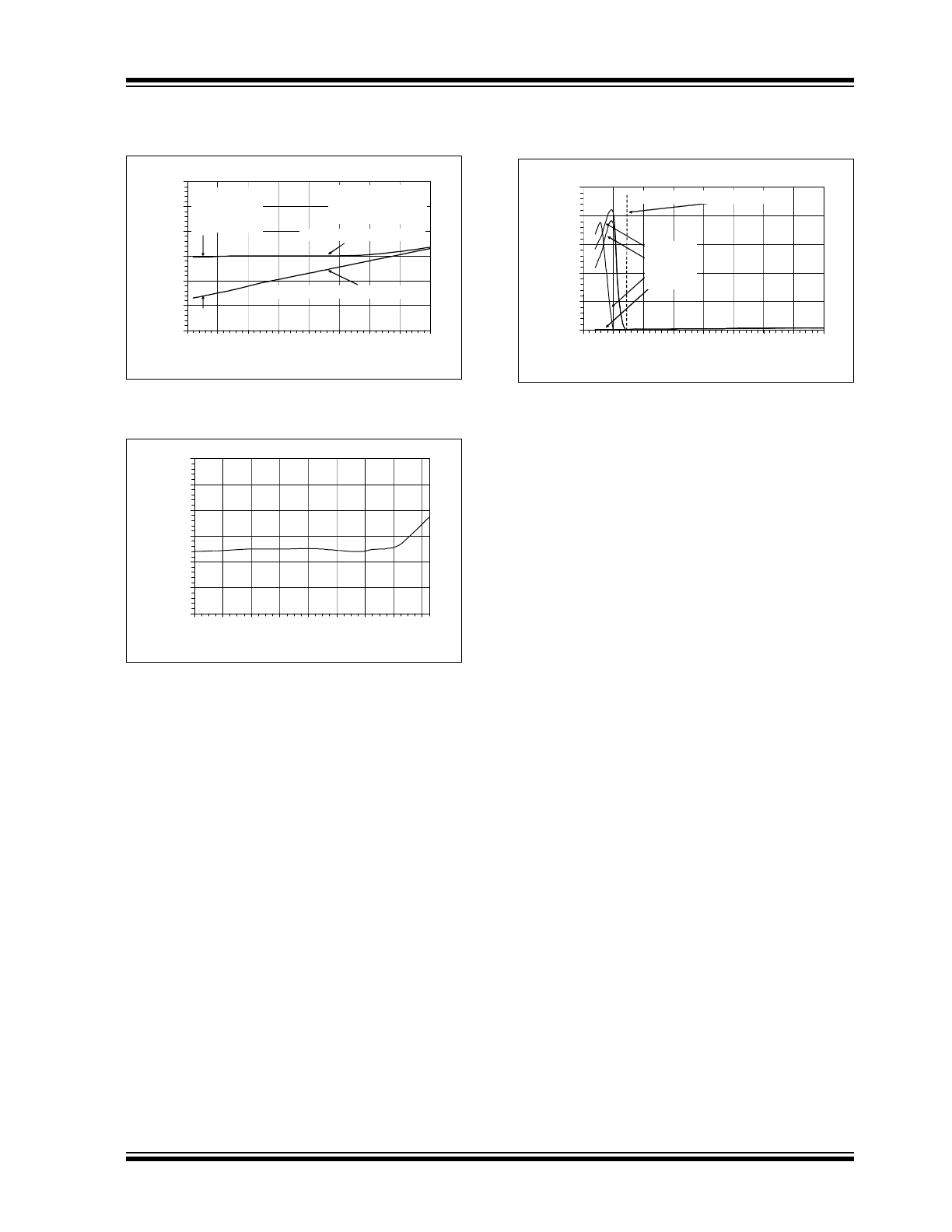
Note: Unless otherwise indicated, V
DD
= 2.7V to 5.5V, GND = Ground, SDA/SCL pulled-up to V
DD
, and
T
A
= -40°C to +125°C.
FIGURE 2-13:
SWP/CWP/PWP High
Voltage Range.
FIGURE 2-14:
Shutdown Current vs.
Temperature.
FIGURE 2-15:
Shutdown Current vs. V
DD
.
0
2
4
6
8
10
12
1.5
2.0
2.5
3.0
3.5
4.0
4.5
5.0
5.5
V
DD
(V)
V
HV
(V
)
Maximum PWP Voltage (V
DD
+ 1V)
Minimum SWP/CWP Voltage
V
HV
applied at A0 pin.
See
Table 5-4
for Pins
A1 and A2 connection
No
SWP/CWP/PWP
function within
this range
0.00
0.50
1.00
1.50
2.00
2.50
3.00
-40
-20
0
20
40
60
80
100 120
T
A
(°C )
I
SH
D
N
(µ
A
)
0
20
40
60
80
100
1.5
2.0
2.5
3.0
3.5
4.0
4.5
5.0
5.5
V
DD
(V)
I
S
HDN
(µ
A)
V
POR_TS
, Sensor in Shutdown Mode
T
A
= -40°C
T
A
= +25°C
T
A
= +85°C
T
A
= +125°C

MCP9843/98243
DS22153C-page 10
© 2009 Microchip Technology Inc.
NOTES: