
2010 Microchip Technology Inc.
DS21996D-page 1
MCP98242
Features:
• Temperature Sensor + 256 Byte Serial EEPROM
• EEPROM for Serial Presence Detect (SPD)
• Optimized for Voltage Range: 3.0V to 3.6V
• Shutdown/Standby Current: 3 µA (maximum)
• 2-wire Interface: I
2
C™/SMBus Compatible
• Available Packages: DFN-8, TDFN-8, UDFN-8,
TSSOP-8
Temperature Sensor Features:
• Temperature-to-Digital Converter
• Operating Current: 200 µA (typical)
• Accuracy:
- ±0.5°C/±1°C (typ./max.)
+75°C to +95°C
- ±1°C/±2°C (typ./max.)
+40°C to +125°C
- ±2°C/±3°C (typ./max.)
-20°C to +125°C
Serial EEPROM Features:
• Operating Current:
- Write
1.1 mA (typical) for 3.5 ms (typical)
- Read
100 µA (typical)
• Permanent and Reversible Software Write-Protect
• Software Write Protection for the Lower 128 Bytes
• Organized as 1 Block of 256 Bytes (256x8)
Typical Applications:
• DIMM Modules
• Laptops, Personal Computers and Servers
• Hard Disk Drives and Other PC Peripherals
Description:
Microchip Technology Inc.’s MCP98242 digital
temperature sensor converts temperature from -40°C
and +125°C to a digital word. This sensor meets
JEDEC Specification JC42.4 Mobile Platform Memory
Module Thermal Sensor Component. It provides an
accuracy of ±0.5°C/±1°C (typical/maximum) from
+75°C to +95°C. In addition, this device has an internal
256 Byte EEPROM which can be used to store memory
module and vendor information.
The MCP98242 digital temperature sensor comes with
user-programmable registers that provide flexibility for
DIMM temperature-sensing applications. The registers
allow user-selectable settings such as Shutdown or
Low-Power modes and the specification of
temperature event and critical output boundaries.
When the temperature changes beyond the specified
boundary limits, the MCP98242 outputs an Event
signal. The user has the option of setting the Event
output signal polarity as either an active-low or
active-high comparator output for thermostat operation,
or as a temperature event interrupt output for
microprocessor-based systems. The Event output can
also be configured as a critical temperature output.
The EEPROM is designed specifically for DRAM
DIMMs (Dual In-line Memory Modules) Serial Presence
Detect (SPD). The lower 128 bytes (address 00h to
7Fh) can be Permanent Write-Protected (PWP) or
Software Reversible Write-Protected (SWP). This
allows DRAM vendor and product information to be
stored and write-protected. The upper 128 bytes
(address 80h to FFh) can be used for general purpose
data storage. These addresses are not write-protected.
This sensor has an industry standard 2-wire, I
2
C/
SMBus compatible serial interface, allowing up to eight
devices to be controlled in a single serial bus. To
maintain interchangeability with the I
2
C/SMBus
interface the electrical specifications are specified with
the operating voltage of 3.0V to 3.6V. In addition, a
40 ms (typical) time out is implemented.
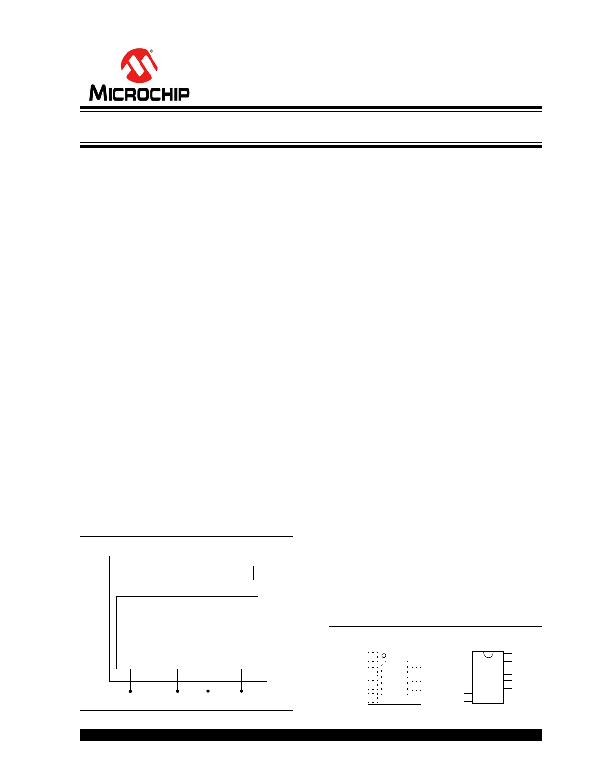
Package Types
Memory
DIMM MODULE
Temperature Sensor + EEPROM
MCP98242
3.3V
DD
_
SPD
SDA
SCL
• ±0.5°C (typ.) Sensor
• 256 Byte EEPROM for SPD
Event
8-Pin DFN/TDFN/UDFN (2x3) *
SDA
GND
Event
SCLK
MCP98242
1
2
3
4
8-Pin TSSOP
A0
V
DD
A1
A2
8
7
6
5
A2
A1
GND
Event
SCLK
1
2
3
4
8
7
6
5 SDA
V
DD
A0
EP
9
* Includes Exposed Thermal Pad (EP); see
Table 3-1
.
Memory Module Temperature Sensor w/EEPROM for SPD

MCP98242
DS21996D-page 2
2010 Microchip Technology Inc.
Notes:
2010 Microchip Technology Inc.
DS21996D-page 3
MCP98242
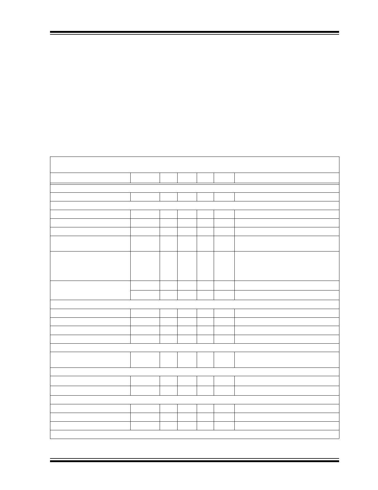
1.0
ELECTRICAL
CHARACTERISTICS
Absolute Maximum Ratings †
V
DD
.................................................................................. 6.0V
Voltage at all Input/Output pins ............... GND – 0.3V to 6.0V
Pin A0 ................................................... GND – 0.3V to 12.5V
Storage temperature .....................................-65°C to +150°C
Ambient temp. with power applied ................-40°C to +125°C
Junction Temperature (T
J
) .......................................... +150°C
ESD protection on all pins (HBM:MM) ................. (4 kV:300V)
Latch-Up Current at each pin (+25°C) ..................... ±200 mA
†Notice: Stresses above those listed under “Maximum
ratings” may cause permanent damage to the device. This is
a stress rating only and functional operation of the device at
those or any other conditions above those indicated in the
operational listings of this specification is not implied.
Exposure to maximum rating conditions for extended periods
may affect device reliability.
DC CHARACTERISTICS
Electrical Specifications: Unless otherwise indicated, V
DD
= 3.0V to 3.6V, GND = Ground, SDA/SCL pulled-up to
V
DD
, and T
A
= -20°C to +125°C.
Parameters
Sym
Min
Typ
Max
Unit
Conditions
Power Supply
Operating Voltage
V
DD
3.0
—
3.6
V
Operating Current
Temperature Sensor
I
DD
—
200
500
µA
EEPROM Inactive
EEPROM write
I
DD
—
1100
2000
µA
Sensor in Shutdown mode (for t
WC
)
EEPROM read
I
DD
—
100
500
µA
Sensor in Shutdown mode
Shutdown Current
I
SHDN
—
1
3
µA
EEPROM Inactive,
Sensor in Shutdown mode
Power-on-Reset (POR)
Threshold
V
POR
—
2.3
—
V
Temperature Sensor (V
DD
falling)
V
POR
—
1.6
—
V
EEPROM (V
DD
falling) (see
Section 5.4
“Summary of Temperature Sensor
Power-on Default”
)
Power Supply Rejection,
T
A
= +25°C
°C/V
DD
—
±0.4
—
°C/V
V
DD
= 3.0V to 3.6V
°C/V
DD
—
±0.15
—
°C
V
DD
= 3.3V+150 mV
PP AC
(0 to 1 MHz)
Temperature Sensor Accuracy
+75°C < T
A
+95°C
T
ACY
-1.0
±0.5
+1.0
°C
+40°C < T
A
+125°C
T
ACY
-2.0
±1
+2.0
°C
-20°C < T
A
+125°C
T
ACY
-3.0
±2
+3.0
°C
T
A
-40°C
T
ACY
—
-2
—
°C
Conversion Time
0.25°C/bit
t
CONV
—
65
125
ms
15 s/sec (typical) (See
Section 5.2.3.3
“Temperature Resolution”
)
Event Output (Open-drain)
High-level Current (leakage)
I
OH
—
—
1
µA
V
OH
= V
DD
Low-level Voltage
V
OL
—
—
0.4
V
I
OL
= 3 mA
EEPROM
Write Cycle (byte/page)
t
WC
—
3
5
ms
—
Endurance T
A
= +25°C
—
1M
—
—
cycles V
DD
= 5V,
Note 1
Write-Protect High Voltage
V
HI_WP
8
—
12
V
Applied at A0 pin,
Note 1
Thermal Response
Note 1:
Characterized but not production tested.
MCP98242
DS21996D-page 4
2010 Microchip Technology Inc.
GRAPHICAL SYMBOL DESCRIPTION
DFN
t
RES
—
0.7
—
s
Time to 63% (89°C)
25°C (Air) to 125°C (oil bath)
TSSOP
t
RES
—
1.4
—
s
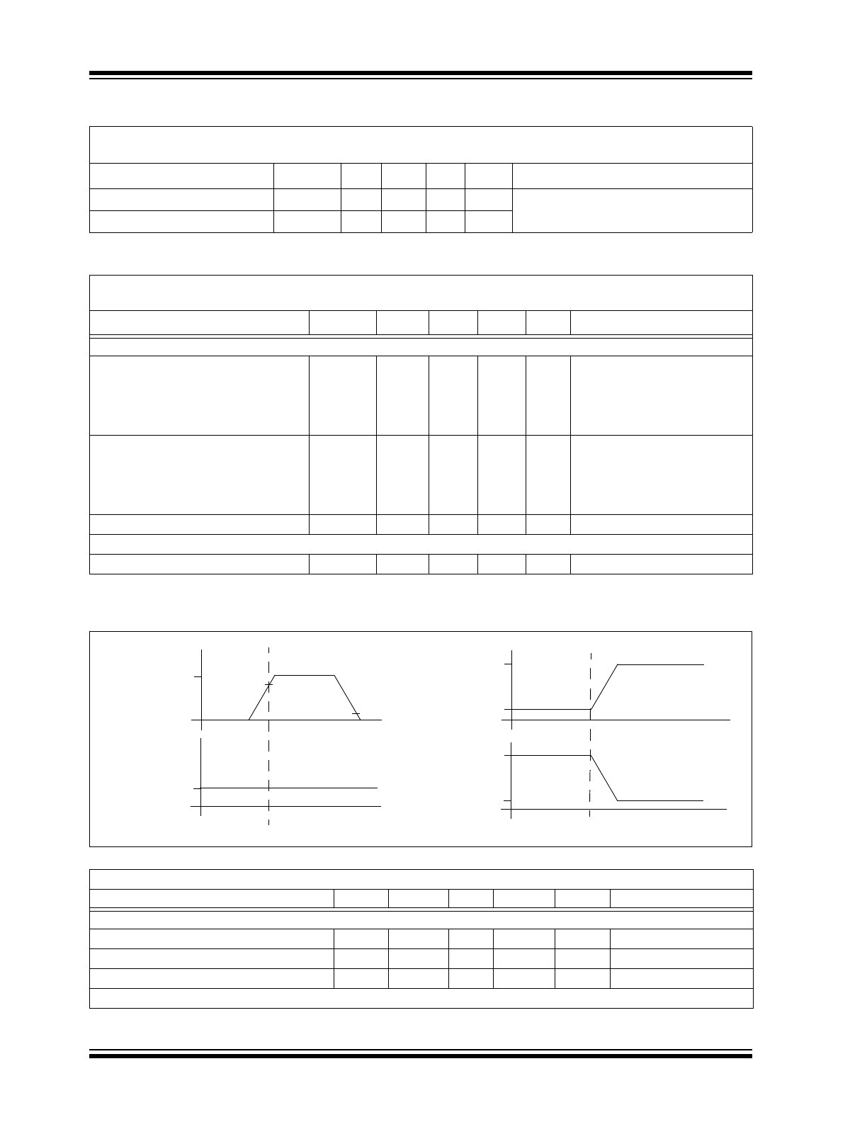
DC CHARACTERISTICS
Electrical Specifications: Unless otherwise indicated, V
DD
= 3.0V to 3.6V, GND = Ground, SDA/SCL pulled-up to
V
DD
, and T
A
= -20°C to +125°C.
Parameters
Sym
Min
Typ
Max
Unit
Conditions
Note 1:
Characterized but not production tested.
INPUT/OUTPUT PIN DC CHARACTERISTICS
Electrical Specifications: Unless otherwise indicated, V
DD
= 3.0V to 3.6V, GND = Ground and
T
A
= -20°C to +125°C.
Parameters
Sym
Min
Typ
Max
Units
Conditions
Serial Input/Output (SCL, SDA, A0, A1, A2)
Input
High-level Voltage
V
IH
2.1
—
—
V
Low-level Voltage
V
IL
—
—
0.8
V
Input Current
I
IN
—
—
±5
µA
Output (SDA)
Low-level Voltage
V
OL
—
—
0.4
V
I
OL
= 3 mA
High-level Current (leakage)
I
OH
—
—
1
µA
V
OH
= V
DD
Low-level Current
I
OL
6
—
—
mA
V
OL
= 0.6V
Capacitance
C
IN
—
5
—
pF
SDA and SCL Inputs
Hysteresis
V
HYST
—
0.5
—
V
Note: The serial inputs do not load the serial bus for V
DD
range of 1.8V to 5.5V.
V
DD
V
IH
V
IL
I
IN
Voltage
Current
time
V
DD
I
OH
Voltage
Current
time
INPUT
OUTPUT
V
OL
I
OL
TEMPERATURE CHARACTERISTICS
Electrical Specifications: Unless otherwise indicated, V
DD
= 3.0V to 3.6V, GND = Ground.
Parameters
Sym
Min
Typ
Max
Units
Conditions
Temperature Ranges
Specified Temperature Range
T
A
-20
—
+125
°C
(
Note 1
)
Operating Temperature Range
T
A
-40
—
+125
°C
Storage Temperature Range
T
A
-65
—
+150
°C
Thermal Package Resistances
Note 1:
Operation in this range must not cause T
J
to exceed Maximum Junction Temperature (+150°C).
2010 Microchip Technology Inc.
DS21996D-page 5
MCP98242
0
TIMING DIAGRAM
Thermal Resistance, 8L-DFN
JA
—
84.5
—
°C/W
Thermal Resistance, 8L-TDFN
JA
—
41
—
°C/W
Thermal Resistance, 8L-TSSOP
JA
—
139
—
°C/W
TEMPERATURE CHARACTERISTICS
Electrical Specifications: Unless otherwise indicated, V
DD
= 3.0V to 3.6V, GND = Ground.
Parameters
Sym
Min
Typ
Max
Units
Conditions
Note 1:
Operation in this range must not cause T
J
to exceed Maximum Junction Temperature (+150°C).
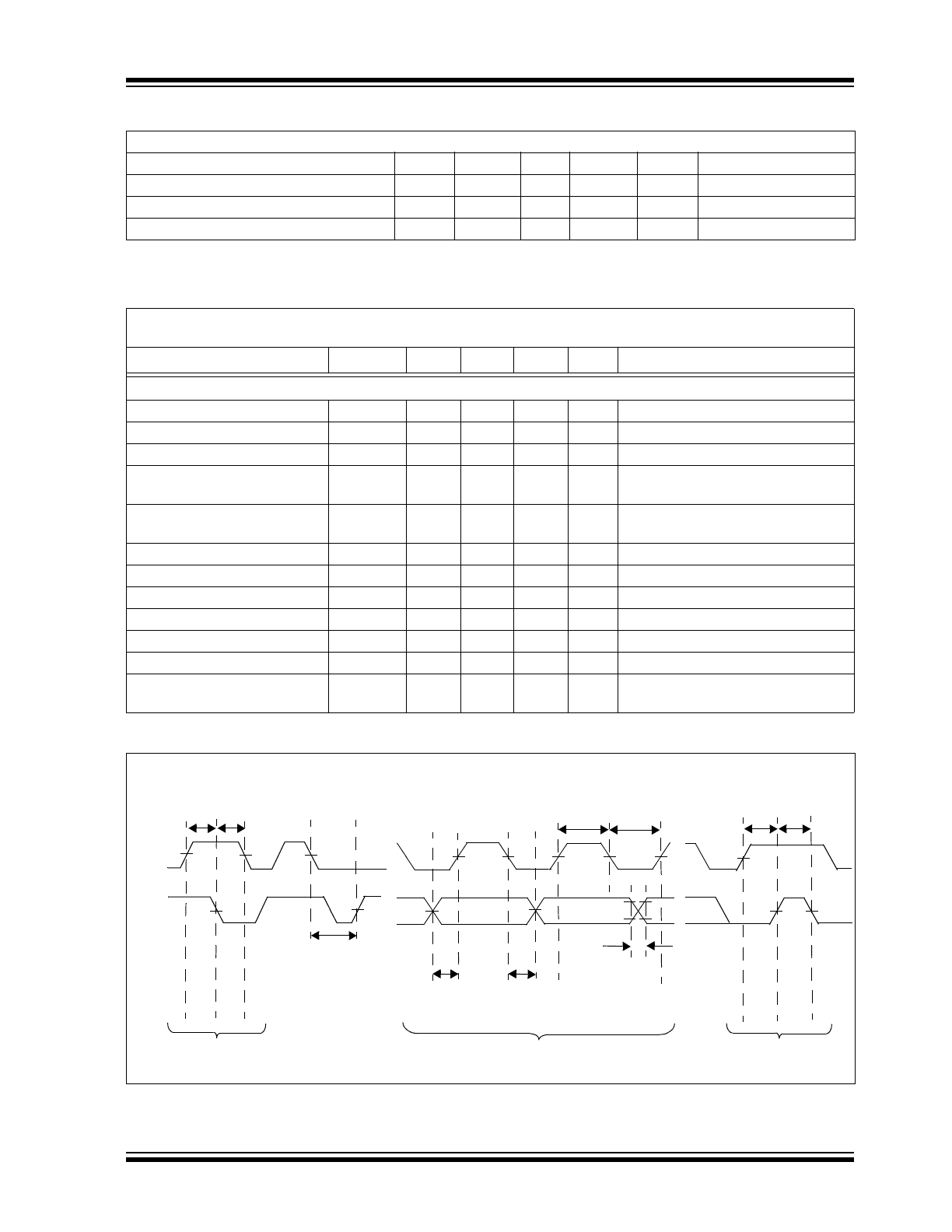
SENSOR AND EEPROM SERIAL INTERFACE TIMING SPECIFICATIONS
Electrical Specifications: Unless otherwise indicated, V
DD
= 3.0V to 3.6V, GND = Ground, T
A
= -20°C to +125°C,
C
L
= 80 pF, and all limits measured to 50% point.
Parameters
Sym
Min
Typ
Max
Units
Conditions
2-Wire I
2
C™/SMBus-Compatible Interface
Serial Port Frequency
f
SC
10
—
100
kHz
I
2
C™/SMBus
Low Clock
t
LOW
4.7
—
—
µs
High Clock
t
HIGH
4.0
—
—
µs
Rise Time
t
R
—
—
1000
ns
(V
IL MAX
- 0.15V) to (V
IH MIN
+
0.15V)
Fall Time
t
F
—
—
300
ns
(V
IH MIN
+ 0.15V) to (V
IL MAX
-
0.15V)
Data Setup Before SCLK High
t
SU-DATA
250
—
—
ns
Data Hold After SCLK Low
t
H-DATA
300
—
—
ns
Start Condition Setup Time
t
SU-START
4.7
—
—
µs
Start Condition Hold Time
t
H-START
4.0
—
—
µs
Stop Condition Setup Time
t
SU-STOP
4.0
—
—
µs
Bus Idle
t
B_FREE
4.7
—
—
µs
Time Out
t
OUT
25
40
50
ms
Temp. Sensor Only (characterized
but not production tested)
t
SU
-S
TA
R
T
t
H
-S
TA
R
T
t
SU
-DA
TA
t
SU
-S
TO
P
t
B-
FRE
E
SC
LK
SDA
t
H-
DA
TA
t
H
IG
H
t
LOW
t
OU
T
t
R
, t
F
Start Condition
Data Transmission
Stop Condition

MCP98242
DS21996D-page 6
2010 Microchip Technology Inc.
NOTES:
2010 Microchip Technology Inc.
DS21996D-page 7
MCP98242
2.0
TYPICAL PERFORMANCE CURVES
Note: Unless otherwise indicated, V
DD
= 3.0V to 3.6V, GND = Ground, SDA/SCL pulled-up to V
DD
, and
T
A
= -20°C to +125°C.
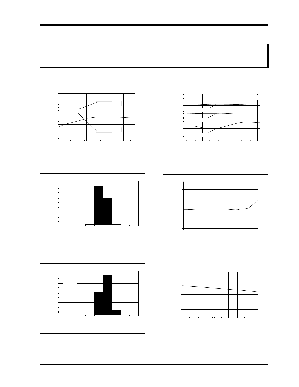
FIGURE 2-1:
Average Temperature
Accuracy.
FIGURE 2-2:
Temperature Accuracy
Histogram, T
A
= +95°C.
FIGURE 2-3:
Temperature Accuracy
Histogram, T
A
= +75°C.
FIGURE 2-4:
Supply Current vs.
Temperature.
FIGURE 2-5:
Shutdown Current vs.
Temperature.
FIGURE 2-6:
Power-on Reset Threshold
Voltage vs. Temperature.
Note:
The graphs and tables provided following this note are a statistical summary based on a limited number of
samples and are provided for informational purposes only. The performance characteristics listed herein
are not tested or guaranteed. In some graphs or tables, the data presented may be outside the specified
operating range (e.g., outside specified power supply range) and therefore outside the warranted range.
-3.0
-2.0
-1.0
0.0
1.0
2.0
3.0
-40
-20
0
20
40
60
80
100 120
T
A
(°C)
Te
mp
er
at
ur
e A
ccu
ra
cy
(
°C
)
V
DD
= 3.0V to 3.6V
Spec. Limits
0%
10%
20%
30%
40%
50%
60%
70%
-1
.0
0
-0
.7
5
-0
.5
0
-0
.2
5
0.
00
0.
25
0.
50
0.
75
1.
00
Temperature Accuracy (°C)
O
ccur
re
nce
s
T
A
= +95°C
V
DD
= 3.3V
221 units
0%
10%
20%
30%
40%
50%
60%
70%
-1
.0
0
-0
.7
5
-0
.5
0
-0
.2
5
0.
00
0.
25
0.
50
0.
75
1.
00
Temperature Accuracy (°C)
O
ccur
re
nce
s
T
A
= +75°C
V
DD
= 3.3V
221 units
1
10
100
1000
10000
-40
-20
0
20
40
60
80
100 120
T
A
(°C)
I
DD
(µ
A
)
V
DD
= 3.3V to 3.6V
EEPROM Write (Sensor in Shutdown Mode)
Sensor (EEPROM Inactive)
EEPROM Read (Sensor in Shutdown Mode)
0.00
0.50
1.00
1.50
2.00
2.50
3.00
-40
-20
0
20
40
60
80
100 120
T
A
(°C )
I
SHD
N
(µ
A
)
V
DD
= 3.0V to 3.6V
0
0.5
1
1.5
2
2.5
3
-40
-20
0
20
40
60
80
100 120
T
A
(°C)
V
PO
R
(V
)
MCP98242
DS21996D-page 8
2010 Microchip Technology Inc.
Note: Unless otherwise indicated, V
DD
= 3.0V to 3.6V, GND = Ground, SDA/SCL pulled-up to V
DD
, and
T
A
= -20°C to +125°C.
FIGURE 2-7:
Event and SDA V
OL
vs.
Temperature.
FIGURE 2-8:
Conversion Rate vs.
Temperature.
FIGURE 2-9:
Power Supply Rejection vs.
Frequency.
FIGURE 2-10:
SDA IOL vs. Temperature.
FIGURE 2-11:
Temperature Accuracy vs.
V
DD
.
FIGURE 2-12:
Package Thermal
Response.
0
0.1
0.2
0.3
0.4
-40
-20
0
20
40
60
80
100 120
T
A
(°C)
E
v
en
t & S
DA V
OL
(V
)
Event
SDA
V
DD
= 3.0V to 3.6V
I
OL
= 3 mA
35
50
65
80
95
110
125
-40
-20
0
20
40
60
80
100 120
T
A
(°C)
t
CONV
(m
s)
V
DD
= 3.0V to 3.6V
-1.0
-0.5
0.0
0.5
1.0
100
1,000
10,000
100,000
1,000,000
Frequency (Hz)
N
o
rm
al
ized
T
e
m
p
.
E
rr
o
r
(°
C
)
Δ°C/ΔV
DD
, V
DD
= 3.3V + 150 mV
PP (AC)
1k
10k
100k
1M
100k
1M
10k
100k
1M
1k
10k
100k
1M
100
1k
10k
100k
1M
T
A
= +25°C
No decoupling capacitor
6
12
18
24
30
36
42
48
-40
-20
0
20
40
60
80
100 120
T
A
(°C)
S
DA I
OL
(m
A
)
V
DD
= 3.0V to 3.6V
V
OL
= 0.6V
-3.0
-2.0
-1.0
0.0
1.0
2.0
3.0
-40
-20
0
20
40
60
80
100 120
T
A
(°C)
T
em
p
er
atu
re A
ccu
ra
cy
(°
C
)
V
DD
= 3.0V
V
DD
= 3.6V
Δ°C/ΔV
DD
= 0.4°C/V
0%
20%
40%
60%
80%
100%
120%
-2
0
2
4
6
8
10
12
14
16
Time (s)
T
h
er
ma
l R
espo
n
se
(%
)
22°C (Air) to 125°C (Oil bath)
TSSOP-8
DFN-8
2010 Microchip Technology Inc.
DS21996D-page 9
MCP98242
3.0
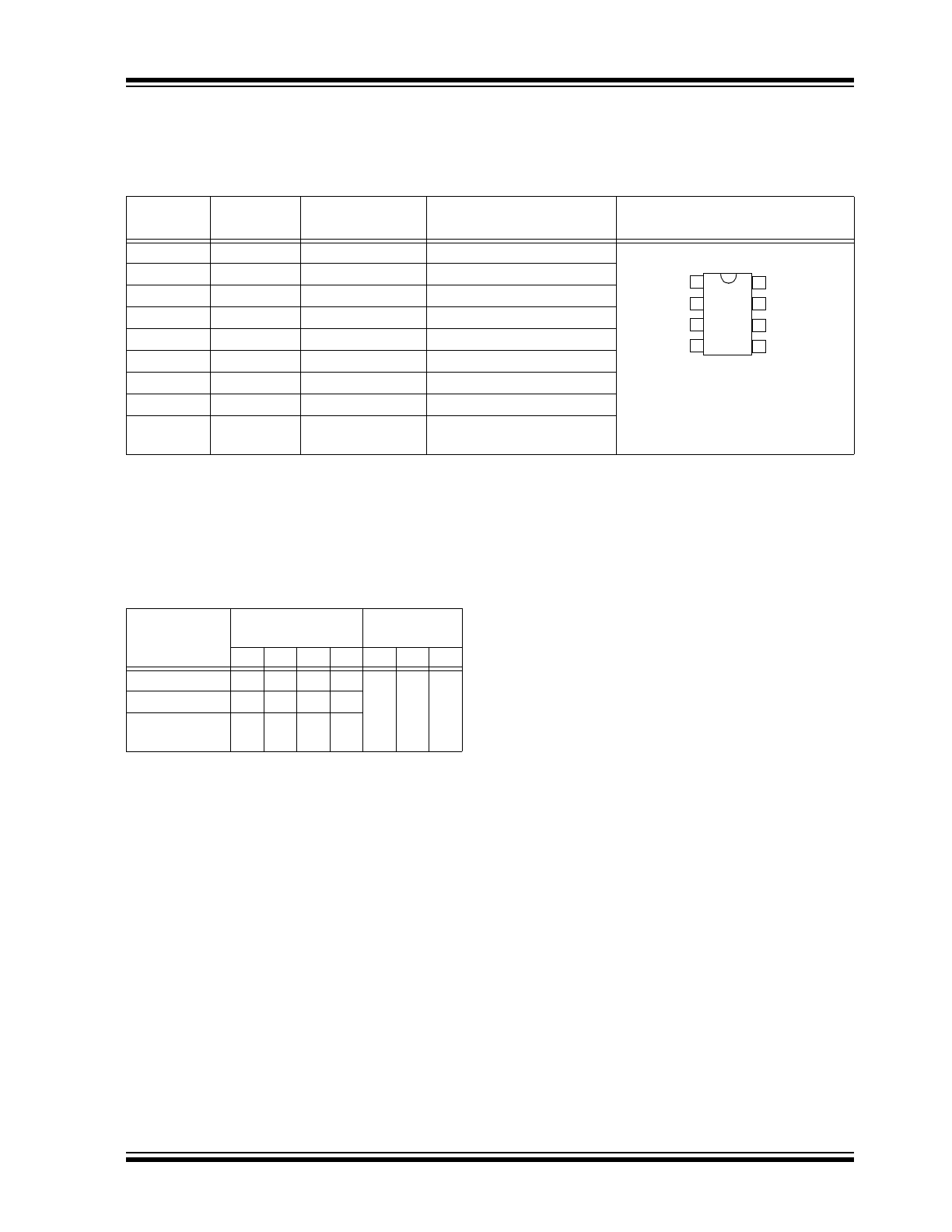
PIN DESCRIPTION
The descriptions of the pins are listed in
Table 3-1
.
TABLE 3-1:
PIN FUNCTION TABLES
3.1
Address Pins (A2, A1, A0)
These pins are device address input pins.
The address pins correspond to the Least Significant
bits (LSb) of address bits. The Most Significant bits
(MSb) (A6, A5, A4, A3). This is shown in
Table 3-2
.
3.2
Ground Pin (GND)
The GND pin is the system ground pin.
3.3
Serial Data Line (SDA)
SDA is a bidirectional input/output pin, used to serially
transmit data to/from the host controller. This pin
requires a pull-up resistor. (See
Section 4.0 “Serial
Communication”
).
3.4
Serial Clock Line (SCLK)
The SCLK is a clock input pin. All communication and
timing is relative to the signal on this pin. The clock is
generated by the host or master controller on the bus.
(See
Section 4.0 “Serial Communication”
).
3.5
Open-Drain Temperature Alert
Output (Event)
The MCP98242 Event pin is an open-drain output. The
device outputs a signal when the ambient temperature
goes beyond the user-programmed temperature limit.
(see
Section 5.2.3 “Event Output Configuration”
).
3.6
Power Pin (V
DD)
V
DD
is the power pin. The operating voltage range, as
specified in the DC electrical specification table, is
applied on this pin.
3.7
Exposed Thermal Pad (EP)
There is an internal electrical connection between the
Exposed Thermal Pad (EP) and the GND pin; they
must be connected to the same potential on the Printed
Circuit Board (PCB).
DFN/TDFN/
UDFN
TSSOP
Symbol
Pin Function
Package Type
1
1
A0
Slave Address
2
2
A1
Slave Address
3
3
A2
Slave Address
4
4
GND
Ground
5
5
SDA
Serial Data Line
6
6
SCLK
Serial Clock Line
7
7
Event
Temperature Alert Output
8
8
V
DD
Power Pin
9
—
EP
Exposed Thermal Pad (EP);
must be connected to V
SS
.
SDA
GND
Event
SCLK
1
2
3
4
8-Pin TSSOP
A0
V
DD
A1
A2
8
7
6
5
TABLE 3-2:
MCP98242 ADDRESS BYTE
Device
Address Code
Slave
Address
A6 A5 A4 A3 A2 A1 A0
Sensor
0
0
1
1
X
X
X
EEPROM
1
0
1
0
EEPROM
Write-Protect
0
1
1
0
Note:
User-selectable address is shown by X.

MCP98242
DS21996D-page 10
2010 Microchip Technology Inc.
NOTES: