
2018 Microchip Technology Inc.
DS20005921A-page 1
MD1715
Features
• Advanced CMOS Technology
• ±4.75 to 12.9V Gate Drive Voltage
• 2A Output Source and Sink Current
• 6.5 ns Rise and Fall Time with 1 nF Load
• 10 ns Propagation Delay
• ±2 ns Matched Delay Times
• 12 Matched Channels
• 1.8V to 3.3V CMOS Logic Interface
• Smart Logic Threshold
• Low-inductance Package
Applications
• Medical Ultrasound Imaging
• Piezoelectric Transducer Drivers
• Metal Flaw Detection
• Non-destructive Testing (NDT)
General Description
The MD1715, paired with Microchip’s TC8020, forms a
2-channel five-level high-voltage high-speed transmit
pulser chip set. The chip set is designed for medical
ultrasound imaging applications but can also be used
for metal flaw detection, NDT and piezoelectric
transducer drivers.
The MD1715 is a 2-channel logic controller circuit with
12 low-impedance MOSFET gate drivers. There are
two sets of control logic inputs—one for Channel A and
one for Channel B. Each channel consists of three pairs
of MOSFET gate drivers. These drivers are designed to
match the drive requirements of Microchip’s TC8020.
The TC8020 is the output stage of the pulser, with six
pairs of MOSFETs. Each pair consists of a P-channel
and an N-channel MOSFET. They are designed to
have the same impedance and can provide typical
peak currents of ±3.5A at 200V.
Package Type
See
Table 2-1
for pin information.
40-lead QFN
(Top view)
1
40
2-Channel 5-Level High-Speed Ultrasound Driver IC
V
DD2
GN2
V
SS
V
DD1
High Speed
Gate Buffers
SP1
DP1
100Ω
DN1
SP2
SN2
DP2
DN2
DP3
DN3
OP1
GP1
ON1
GN1
Control
Logic
and
Level
Translation
VLL/EN
SEL
POS
NEG
GND
OP2
GP2
ON2
OP3
GP3
GN3
ON3
SN3
SP3
V
PP2
V
NN2
V
NN1
MD1715
1 OF 2-CH
TC8020
6 of 12-FETs
V
PP1
VDD1
VDD2
-12V
VSS
AVSS
-12V
GND
+12V +12V
AVDD
+12V
PAD
PAD
V
DD2
V
DD1
V
DD1
High Speed
Gate Buffers
SN1
MD1715
DS20005921A-page 2
2018 Microchip Technology Inc.
Functional Block Diagram
2018 Microchip Technology Inc.
DS20005921A-page 3
MD1715
Typical Application Circuit
10nF
10nF
10nF
10nF
10nF
10nF
10nF
10nF
TX(B)
TX(A)
TC8020
MD1715
AVDD
SELA
POSA
NEGA
POSB
NEGB
SELB
OP1A
ON1A
OP2A
ON2A
OP3A
ON3A
OP1B
ON1B
OP2B
ON2B
OP3B
ON3B
GP1
GN1
GP2
GN2
GP3
GN3
GP4
GN4
GP5
GN5
GP6
GN6
AGND
VLL/EN
+12V
GND
AVSS
(SUB)
VSS
1.8 to 3.3V
CMOS
Input Logic
VDD1
VDD2
-12V
+12V
+12V
+3.3V
-12V
VPP2
SP2
VPP1
SP1
SP3
SP4
SP5
SP6
SN3
SN2
SN1
VNN1
VNN2
SN5
SN4
SN6
PAD
DP1
DN1
DP2
DN2
DP3
DN3
DP4
DN4
DP5
DN5
DP6
DN6
MD1715
DS20005921A-page 4
2018 Microchip Technology Inc.
1.0
ELECTRICAL CHARACTERISTICS
Absolute Maximum Ratings†
GND and AGND, Ground .......................................................................................................................................... 0V
Logic Input Pin, V
LL
................................................................................................................................ –0.5V to +5.5V
Positive Gate Drive Supply, AV
DD
, V
DD
1, V
DD
2
................................................................................... –0.5V to +14.5V
Negative Gate Drive Supply, AV
SS,
V
SS
............................................................................................... –14.5V to +0.5V
Operating Junction Temperature, T
J
....................................................................................................... 0°C to +125°C
Storage Temperature, T
S
..................................................................................................................... –65°C to +150°C
Power Dissipation:
40-lead QFN (
Note 1
) ................................................................................................................................. 1.3W
† Notice: Stresses above those listed under “Absolute Maximum Ratings” may cause permanent damage to the
device. This is a stress rating only, and functional operation of the device at those or any other conditions above those
indicated in the operational sections of this specification is not intended. Exposure to maximum rating conditions for
extended periods may affect device reliability.
Note 1:
OPERATING SUPPLY VOLTAGES AND CURRENTS
Electrical Specifications for Operating Supply Currents: Over operating conditions unless otherwise specified,
V
LL
= 3.3V, AV
DD
= V
DD1
= V
DD2
= +12V, AV
SS
= V
SS
= –12V, T
A
= 25°C
Parameter
Sym.
Min.
Typ.
Max. Unit
Conditions
Logic Supply
V
LL
1.8
3.3
3.6
V
Positive Analog Supply
AV
DD
8
—
12.9
V
AV
DD
≥ (V
DD
1 or V
DD
2)
Positive Gate Drive Supply
V
DD
2, V
DD
1
4.75
—
12.9
V
Negative Gate Drive Supply
AV
SS
, V
SS
–12.9
—
–4.75
V
Logic Reference Current
I
VLL
—
10
—
µA V
LL
= 3.3V
AV
DD
Power-down Current
I
AVDDQ
—
0.4
—
mA
EN = 0, all inputs low
V
SS
Power-down Current
I
VSSQ
—
0.1
—
mA
V
DD1
Power-down Current
I
VDD1Q
—
10
25
µA
EN = 0, all inputs low
V
DD2
Power-down Current
I
VDD2Q
—
10
25
µA
AV
DD
Power-up Current
I
AVDDEN
—
2
3
mA
EN = 1, all inputs low
V
SS
Power-up Current
I
VSSEN
—
0.7
1
mA
V
DD
1 Power-up Current
I
VDD1EN
—
10
—
µA
EN = 1, all inputs low
V
DD
2 Power-up Current
I
VDD2EN
—
10
—
µA
AV
DD
CW 5 MHz Current
I
AVDDCW
—
10
—
mA A and B Channels on
at 5 MHz, no load,
V
DD
1 = 12V, V
DD
2 = 5V
V
SS
CW 5 MHz Current
I
VSSCW
—
5
—
mA
V
DD
1 CW 5 MHz Current
I
VDD1CW
—
25
—
mA
A and B Channels on
at 5 MHz, no load,
V
DD
1 = 5V, V
DD
2 = 12V
V
DD
2 CW 5 MHz Current
I
VDD2CW
—
25
—
mA
A and B Channels on
at 5 MHz, no load,
V
DD
1 = 12V, V
DD
2 = 5V
1 oz. four-layer 3 inches x 4 inches PCB
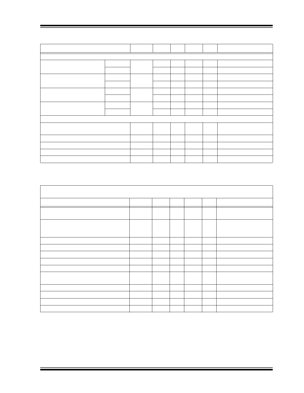
DC ELECTRICAL CHARACTERISTICS
Parameter
Sym.
Min.
Typ.
Max.
Unit
Conditions
P-CHANNEL AND N-CHANNEL GATE DRIVER OUTPUTS
Output Sink Resistance
P-Channel
R
SINK
—
5
6
Ω
I
SINK
= 100 mA
N-Channel
—
5
6
Ω
I
SINK
= 100 mA
Output Source Resistance
P-Channel
R
SOURCE
—
5
6
Ω
I
SOURCE
= 100 mA
N-Channel
—
5
6
Ω
I
SOURCE
= 100 mA
Peak Output Sink Current
P-Channel
I
SINK
1.7
2
—
A
N-Channel
1.7
2
—
A
Peak Output Source Current
P-Channel
I
SOURCE
1.7
2
—
A
N-Channel
1.7
2
—
A
LOGIC INPUTS
Chip Disable Low Voltage
V
ENL
0
—
0.3
V
VLL/EN is a dual function
pin
Input Logic High Voltage
V
IH
0.8 V
LL
—
V
LL
V
Input Logic Low Voltage
V
IL
0
—
0.2 V
LL
V
Input Logic High Current
I
IH
—
—
1
µA
Input Logic Low Current
I
IL
–1
—
—
µA
AC ELECTRICAL CHARACTERISTICS
Electrical Specifications: Over operating conditions unless otherwise specified, V
LL
= 3.3V,
AV
DD
= V
DD
1 = V
DD
2 = +12V, AV
SS
= V
SS
= –12V, T
A
= 25°C
Parameter
Sym.
Min.
Typ.
Max.
Unit
Conditions
Input Rise and Fall Time
t
irf
—
—
10
ns
Logic input edge speed
requirement
Output Rise Time
t
r
—
6.5
—
ns
1 nF load, input signal
rise/fall time 2 ns (
Timing
Waveforms
)
Output Fall Time
t
f
—
6.5
—
ns
Output Rise Delay
t
dr
—
10
—
ns
Output Fall Delay
t
df
—
10
—
ns
Rise and Fall Time Matching
|t
r
–t
f
|
—
1
—
—
For each channel
Propagation Delay Matching
|t
dr
–t
df
|
—
1
—
—
Delay Time Matching
t
dm
—
±2
—
ns
Channel to channel and
device to device
Output Jitter
∆t
j
—
20
—
ps
V
DD
= 10V
IC Enable Time
t
EN
_
ON
—
25
50
μs
IC Disable Time
t
EN
_
OFF
—
0.5
2
μs
Second Harmonic Distortion
HD2
–40
—
—
dB
2018 Microchip Technology Inc.
DS20005921A-page 5
MD1715

MD1715
DS20005921A-page 6
2018 Microchip Technology Inc.
TEMPERATURE SPECIFICATIONS
Parameter
Sym.
Min.
Typ.
Max.
Unit
Conditions
TEMPERATURE RANGE
Operating Junction Temperature
T
J
–0
—
+125
°C
Storage Temperature
T
S
–65
—
+150
°C
PACKAGE THERMAL RESISTANCE
40-lead QFN
JA
—
24
—
°C/W
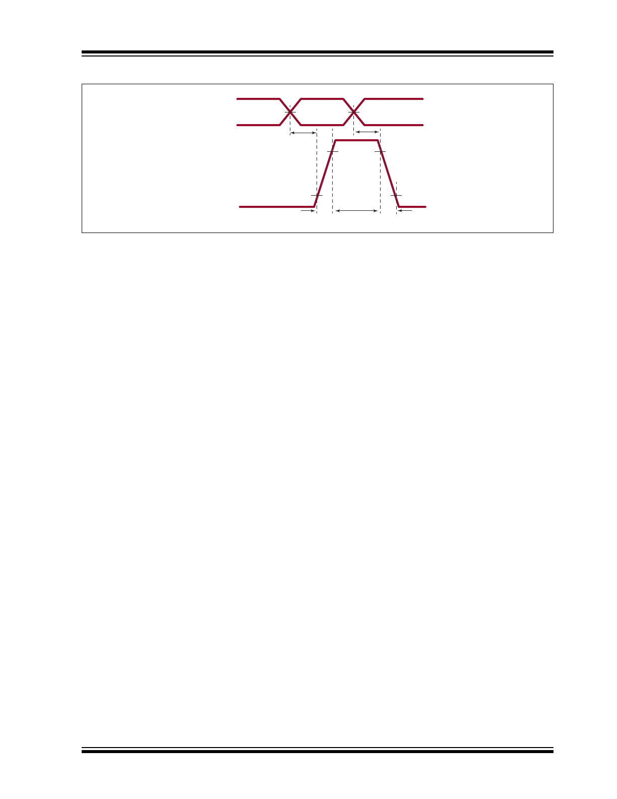
t
df
50%
10%
50%
Input
Output
0V
t
dr
V
DD
t
r
t
f
90%
2018 Microchip Technology Inc.
DS20005921A-page 7
MD1715
Timing Waveforms

MD1715
DS20005921A-page 8
2018 Microchip Technology Inc.
2.0
PIN DESCRIPTION
The details on the pins of MD1715 are listed on
Table 2-1
. See
Package Type
for the location of pins.
TABLE 2-1:
PIN FUNCTION TABLE
Pin Number
Pin Name
Description
1
SELA
SEL input logic control for Channel A. See
Table 3-1
.
2
POSA
POS input logic control for Channel A. See
Table 3-1
.
3
NEGA
NEG input logic control for Channel A. See
Table 3-1
.
4
VLL/EN
Logic High reference voltage and chip enable input
5
AVDD
Positive supply voltage of analog circuitry. AVDD should be at the same or higher
potential than the highest voltages of VDD1 or VDD2.
6
AGND
Digital ground
7
AVSS
Negative supply voltage of analog circuitry and connection of IC substrate.
Should be at the same potential as VSS.
8
SELB
SEL input logic control for Channel B. See
Table 3-2
.
9
POSB
POS input logic control for Channel B. See
Table 3-2
.
10
NEGB
NEG input logic control for Channel B. See
Table 3-2
.
11
VDD2
Positive supply voltage of the gate drivers for the output stages OP1 and ON1 in
Channel A and Channel B. VDD2 can be at a different voltage than VDD1.
12
OP1B
First output P-channel gate driver for Channel B
13
VDD1
Positive supply voltage of the gate drivers for the output stages OP2, ON2 and
ON3 in Channel A and Channel B. VDD1 can be at a different voltage than
VDD2.
14
GND
Power ground
15
OP2B
Second output P-channel gate driver for Channel B
16
VDD2
Positive supply voltage of the gate drivers for the output stages OP1 and ON1 in
Channel A and Channel B. VDD2 can be at a different voltage than VDD1.
17
ON1B
First output N-channel gate driver for Channel B
18
GND
Power ground
19
VDD1
Positive supply voltage of the gate drivers for the output stages OP2, ON2 and
ON3 in Channel A and Channel B. VDD1 can be at a different voltage than
VDD2.
20
ON2B
Second output N-channel gate driver for Channel B
21
GND
Power ground
22
ON3B
Damping output N-channel gate driver for Channel B
23
VSS
Negative supply voltage for the gate drive of OP3. Should be the same voltage as
AVSS.
24
OP3B
Damping output P-channel gate driver for Channel B
25
GND
Power ground
26
VSS
Negative supply voltage for gate drive of OP3. Should be the same voltage as
AVSS.
27
OP3A
Damping output P-channel gate driver for Channel A
28
GND
Power ground
2018 Microchip Technology Inc.
DS20005921A-page 9
MD1715
29
GND
Power ground
30
ON3A
Damping output N-channel gate driver for Channel A
31
ON2A
Second output N-channel gate driver for Channel A
32
VDD1
Positive supply voltage of the gate drivers for the output stages OP2, ON2 and
ON3 in Channel A and Channel B. VDD1 can be at a different voltage than
VDD2.
33
GND
Power ground
34
ON1A
First output N-channel gate driver for Channel A
35
VDD2
Positive supply voltage of the gate drivers for the output stages OP1 and ON1 in
Channel A and Channel B. VDD2 can be at a different voltage than VDD1.
36
OP2A
Second output P-channel gate driver for Channel A
37
GND
Power ground
38
VDD1
Positive supply voltage of the gate drivers for the output stages OP2, ON2 and
ON3 in Channel A and Channel B. VDD1 can be at a different voltage than
VDD2.
39
OP1A
First output P-channel gate driver for Channel A
40
VDD2
Positive supply voltage of the gate drivers for the output stages OP1 and ON1 in
Channel A and Channel B. VDD2 can be at a different voltage than VDD1.
Center Pad
Thermal Pad
IC substrate, must connect to AVSS externally
TABLE 2-1:
PIN FUNCTION TABLE (CONTINUED)
Pin Number
Pin Name
Description
MD1715
DS20005921A-page 10
2018 Microchip Technology Inc.
3.0
FUNCTIONAL DESCRIPTION
TC8020
GN1
GN2
NC
GN3
GP3
NC
SN3
SN6
NC
GP6
GN6
NC
GN5
GN4
GP5
GP4
NC
SN5
NC
SN4
NC
VSUB
NC
SP4
NC
SP5
NC
NC
DN1
DP1
DN2
DP2
DN3
DP3
SP3
SP6
DN6
DP6
DN5
DP5
DN4
DP4
GP2
GP1
NC
SN2
NC
SN1
NC
VSUB
NC
SP1
NC
SP2
NC
NC
MD1715
SELA
POSA
NEGA
VLL/EN
AVDD
AGND
AVSS
SELB
POSB
NEGB
VDD2
OP1A
VDD1
GND
OP2A
VDD2
ON1A
GND
VDD1
ON2A
ON3A
GND
GND
OP3A
VSS
GND
OP3B
VSS
ON3B
GND
VDD2
OP1B
VDD1
GND
OP2B
VDD2
ON1B
GND
VDD1
ON2B
TX(A)
TX(B)
FIGURE 3-1:
Circuit Pin Layout.