
2017 Microchip Technology Inc.
DS20005713B-page 1
MD1213
Features
• 6 ns Rise and Fall Time with 1000 pF Load
• 2A Peak Output Source and Sink Currents
• 1.8V to 5V Input CMOS Compatible
• 4.5V to 13V Total Supply Voltage
• Smart Logic Threshold
• Low-Jitter Design
• Two Matched Channels
• Outputs can Swing Below Ground
• Low-Inductance Package
• Thermally Enhanced Package
Applications
• Medical Ultrasound Imaging
• Piezoelectric Transducer Drivers
• Non-Destructive Testing
• PIN Diode Driver
• CCD Clock Driver/Buffer
• High-Speed Level Translator
General Description
The MD1213 is a high-speed dual-MOSFET driver. It is
designed to drive high-voltage P-channel and
N-channel MOSFETs for medical ultrasound and other
applications requiring a high-output current for a
capacitive load. The high-speed input stage of the
MD1213 can operate from 1.8V to 5V logic interface
with an optimum operating input signal range of 1.8V to
3.3V. An adaptive threshold circuit is used to set the
level translator switch threshold to the average of the
input logic 0 and logic 1 levels. The input logic levels
may be ground referenced even though the driver is
putting out bipolar signals. The level translator uses a
proprietary circuit, which provides DC coupling
together with high-speed operation.
The output stage of the MD1213 has separate power
connections enabling the output signal L and H levels
to be chosen independently from the supply voltages
used for the majority of the circuit. As an example, the
input logic levels may be 0V and 1.8V, the control logic
may be powered by +5V to –5V, and the output L and
H levels may be varied anywhere over the range of –5V
to +5V. The output stage is capable of peak currents of
up to ±2A, depending on the supply voltages used and
load capacitance present.
The OE pin serves a dual purpose. First, its
logic H level is used to compute the threshold voltage
level for the channel input level translators. Second,
when OE is low, the outputs are disabled with the A
output high and the B output low. This assists in
properly pre-charging the AC coupling capacitors that
may be used in series in the gate drive circuit of an
external PMOS and NMOS transistor pair.
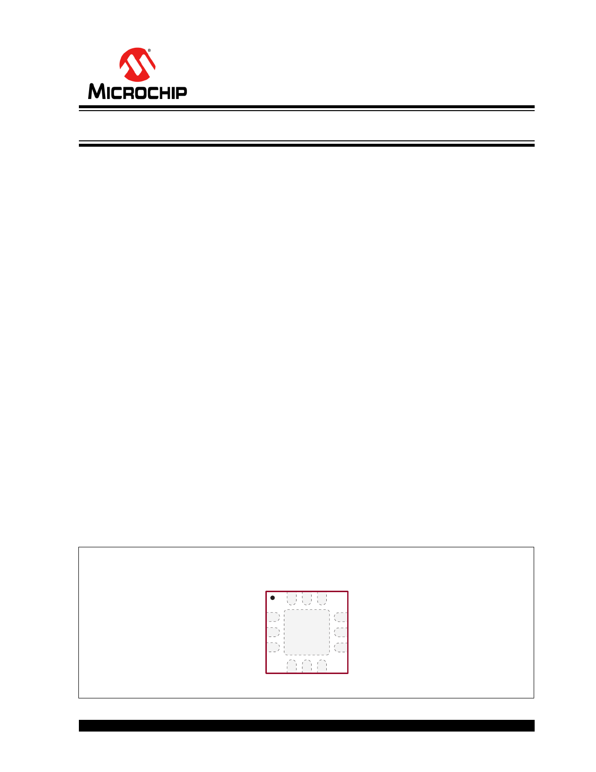
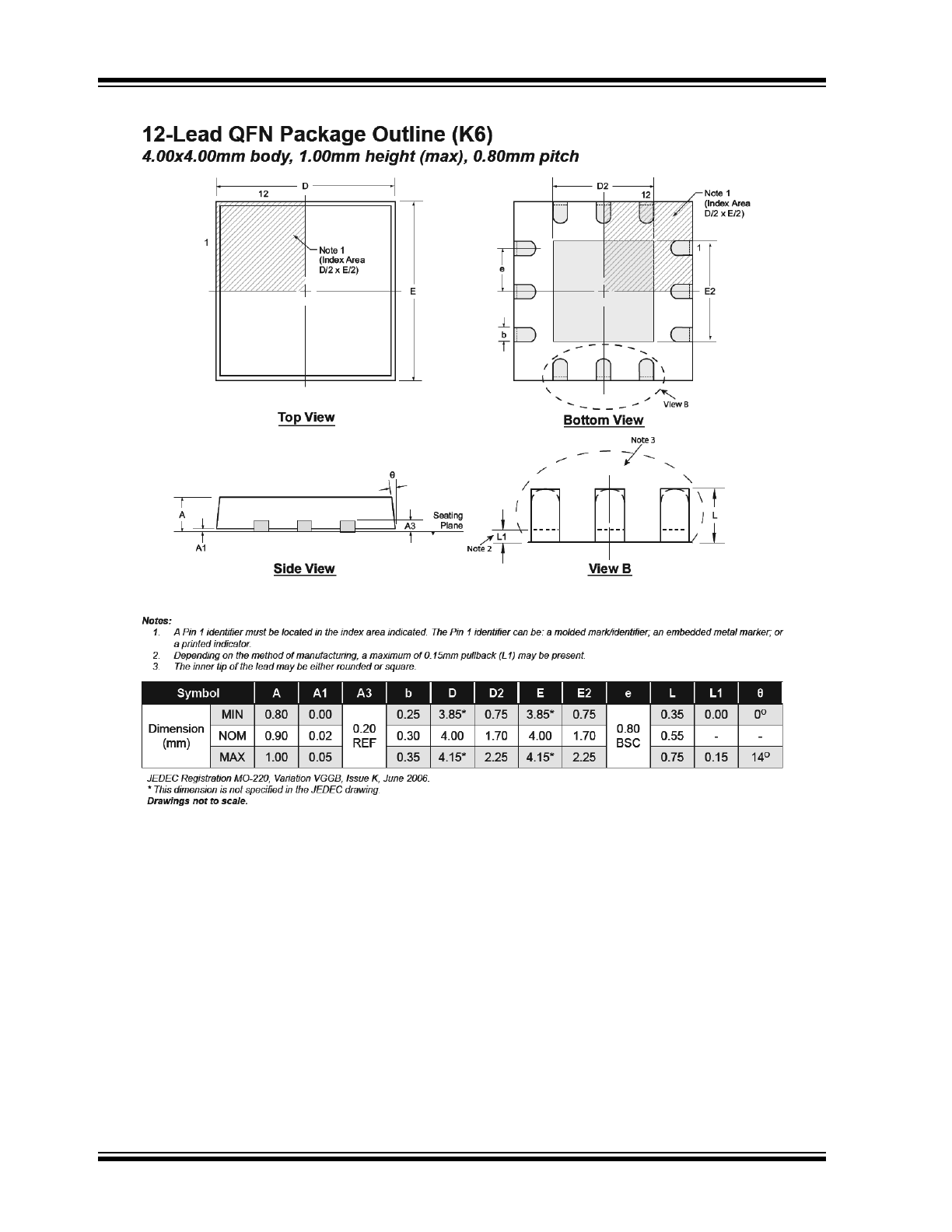
Package Type
12-lead QFN
(Top view)
See
Table 2-1
for pin information.
1
12
High-Speed Dual-MOSFET Driver
MD1213
DS20005713B-page 2
2017 Microchip Technology Inc.
Functional Block Diagram
VDD2
VH
VL
INA
OUTA
INB
OE
V
SS
2
VL
OUTB
VSS2
V
DD
2
VH
VSS1
GND
VDD1
SUB
Level
Shifter
Level
Shifter
Level
Shifter
2017 Microchip Technology Inc.
DS20005713B-page 3
MD1213
Typical Application Circuit
VDD2
VH
VL
INA
OUTA
INB
OE
V
SS
2
VL
OUTB
VSS2
V
DD
2
VH
VSS1
GND
VDD1
TC6320
1.0µF
-100V
To
Piezoelectric
Transducer
10nF
10nF
0.47µF
+5.0V
MD1213
3.3V
CMOS
Logic
Inputs
0.47µF
-5.0V
1.0µF
+100V
Level
Shifter
Level
Shifter
Level
Shifter
MD1213
DS20005713B-page 4
2017 Microchip Technology Inc.
1.0
ELECTRICAL CHARACTERISTICS
Absolute Maximum Ratings†
Level Translator Supply Voltage, V
DD
–V
SS
...........................................................................................–0.5V to +13.5V
Output High Supply Voltage, V
H
................................................................................................. V
L
–0.5V to V
DD
+ 0.5V
Output Low Supply Voltage, V
L
................................................................................................... V
SS
–0.5V to V
H
+ 0.5V
Low-Side Supply Voltage, V
SS
................................................................................................................. –7V to + 0.5V
Logic Input Pins .......................................................................................................................... V
SS
–0.5V to GND +7V
Maximum Junction Temperature, T
J
.................................................................................................................. +125°C
Operating Ambient Temperature, T
A
..................................................................................................... –40°C to +85°C
Storage Temperature, T
S
......................................................................................................................–65°C to +150°C
ESD Rating (
Note 1
) ............................................................................................................................... ESD Sensitive
Note 1: Device is ESD sensitive. Handling precautions are recommended.
† Notice: Stresses above those listed under “Absolute Maximum Ratings” may cause permanent damage to the
device. This is a stress rating only, and functional operation of the device at those or any other conditions above those
indicated in the operational sections of this specification is not intended. Exposure to maximum rating conditions for
extended periods may affect device reliability.
DC ELECTRICAL CHARACTERISTICS
Electrical Specifications: Over operating conditions unless otherwise specified, V
H
= V
DD
1 = V
DD
2 = 12V,
V
L
= V
SS
1
= V
SS
2 = 0V, V
OE
= 3.3V, T
A
= 25°C.
Parameter
Sym.
Min.
Typ.
Max.
Unit
Conditions
Level Translator
Supply Voltage
V
DD
–V
SS
4.5
—
13
V
2.5V ≤ V
DD
≤ 13V
Level Translator Negative
Supply Voltage
V
SS
–5.5
—
0
V
Output High Supply Voltage
V
H
V
SS
+2
—
V
DD
V
Output Low Supply Voltage
V
L
V
SS
—
V
DD
–2
V
V
DD
1 Quiescent Current
I
DD1Q
—
0.55
—
mA
No input transitions
V
DD
2 Quiescent Current
I
DD2Q
—
—
10
µA
V
H
Quiescent Current
I
HQ
—
—
10
µA
V
DD
1 Average Current
I
DD
1
—
0.88
—
mA
One channel on at 5 MHz,
no load
V
DD
2 Average Current
I
DD
2
—
6.6
—
mA
V
H
Average Current
I
H
—
23
—
mA
Input Logic Voltage High
V
IH
V
OE
–0.3
—
5
V
For logic inputs INA and INB
Input logic Voltage Low
V
IL
0
—
0.3
V
Input Logic Current High
I
IH
—
—
1
µA
Input Logic Current Low
I
IL
—
—
1
µA
OE Input Logic Voltage High
V
IH
1.8
—
5
V
For logic input OE
OE Input Logic Voltage Low
V
IL
0
—
0.3
V
OE Input Logic Impedance
to GND
R
IN
12
20
30
KΩ
Logic Input Capacitance
C
IN
—
5
10
pF
All inputs
Output Sink Resistance
R
SINK
—
—
12.5
Ω
I
SINK
= 50 mA
Output Source Resistance
R
SOURCE
—
—
12.5
Ω
I
SOURCE
= 50 mA
Peak Output Sink Current
I
SINK
—
2
—
A
Peak Output Source Current
I
SOURCE
—
2
—
A
2017 Microchip Technology Inc.
DS20005713B-page 5
MD1213
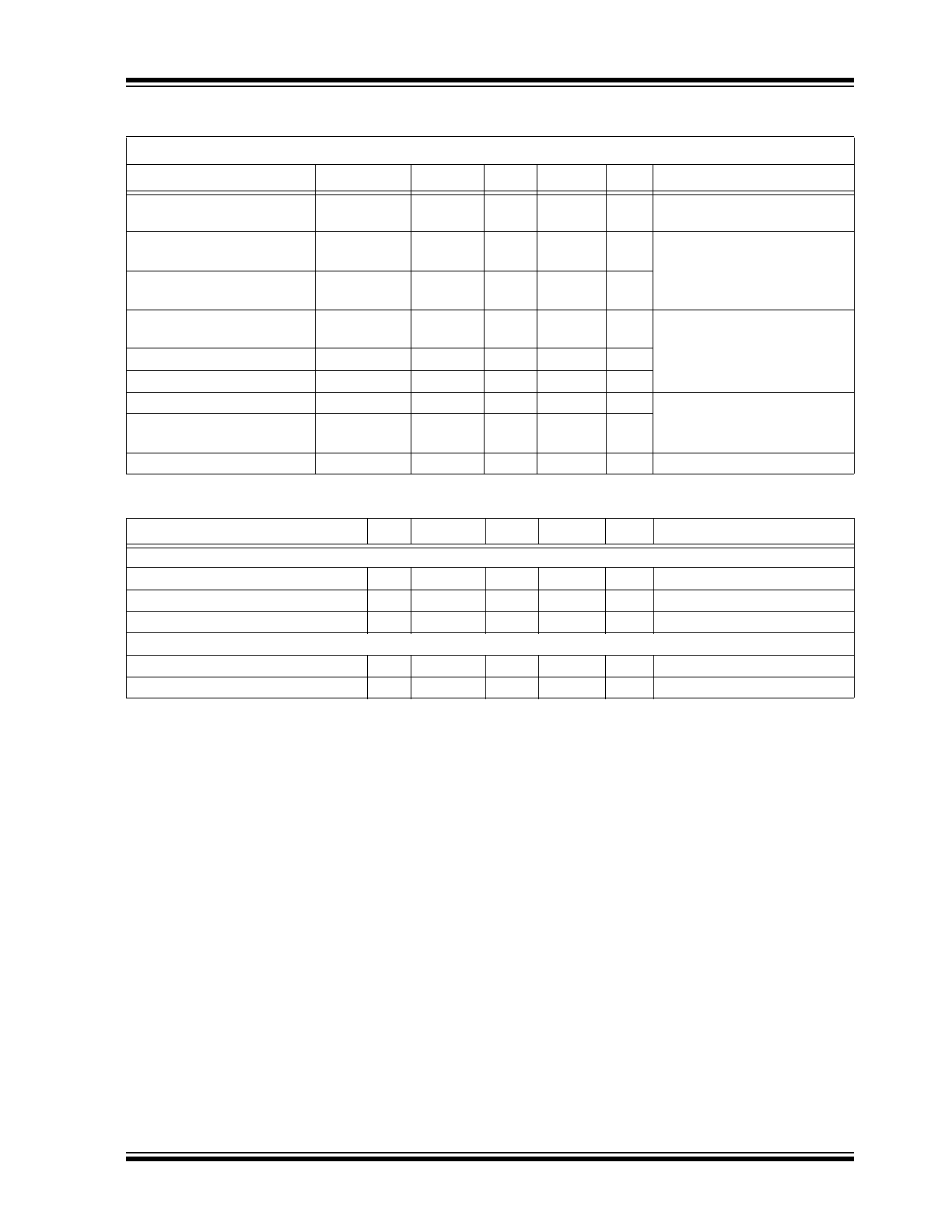
TEMPERATURE SPECIFICATIONS
Note 1: On an 1 oz. 4-layer 3” x 4” PCB with thermal pad and thermal via array
AC ELECTRICAL CHARACTERISTICS
Electrical Specifications: V
H
= V
DD
1 = V
DD
2 = 12V, V
L
= V
SS
1 = V
SS
2 = 0V, V
OE
= 3.3V, T
A
= 25°C.
Parameter
Sym.
Min.
Typ.
Max.
Unit
Conditions
Inputs or OE Rise
and Fall Time
t
irf
—
—
10
ns
Logic input edge speed
requirement
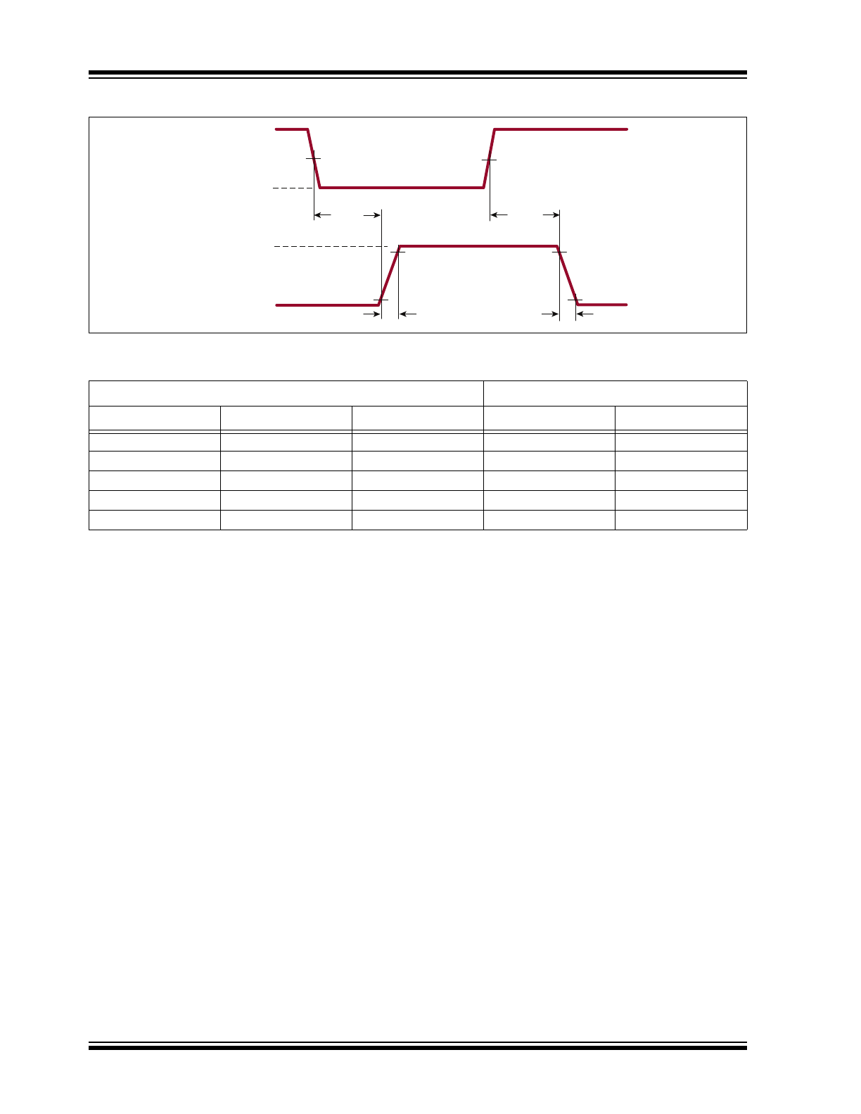
Propagation Delay when
Output is from Low to High
t
PLH
—
7
—
ns
C
LOAD
= 1000 pF, input signal
rise/fall time of 2 ns (See
Tim-
ing Diagram
and
Figure 3-1
.)
Propagation Delay when
Output is from High to Low
t
PHL
—
7
—
ns
Propagation Delay OE
to Outputs
t
POE
—
9
—
ns
C
LOAD
= 1000 pF, input signal
rise/fall time of 2 ns (See
Tim-
ing Diagram
.)
Output Rise Time
t
r
—
6
—
ns
Output Fall Time
t
f
—
6
—
ns
Rise and Fall Time Matching
l t
r
–t
f
l
—
1
—
ns
For each channel
Propagation Low to High and
High-to-low Matching
l t
PLH
–t
PHL
l
—
1
—
ns
Propagation Delay Match
∆t
dm
—
±2
—
ns
Device-to-device delay match
Parameter
Sym.
Min.
Typ.
Max.
Unit
Conditions
TEMPERATURE RANGE
Maximum Junction Temperature
T
J
—
—
+125
°C
Operating Ambient Temperature
T
A
–40
—
+85
°C
Storage Temperature
T
S
–65
—
+150
°C
PACKAGE THERMAL RESISTANCE
12-lead QFN
JA
—
47
—
°C/W
Note 1
Thermal Resistance to Case
θ
JC
—
7
—
°C/W
MD1213
DS20005713B-page 6
2017 Microchip Technology Inc.
Timing Diagram
TABLE 1-1:
TRUTH FUNCTION TABLE
Logic Input
Output
OE
INA
INB
OUTA
OUTB
H
L
L
V
H
V
H
H
L
H
V
H
V
L
H
H
L
V
L
V
H
H
H
H
V
L
V
L
L
X
X
V
H
V
L
IN
t
PLH
10%
OUT
t
PHL
t
r
90%
10%
t
f
3.3V
0V
0V
90%
50%
50%

2017 Microchip Technology Inc.
DS20005713B-page 7
MD1213
2.0
PIN DESCRIPTION
The details on the pins of MD1213 are listed on
Table 2-1
. See
Package Type
for the location of pins.
TABLE 2-1:
PIN FUNCTION TABLE
Pin Number
Pin Name
Description
1
INA
Logic input. Controls OUTA when OE is high. Input logic high will cause the output to
swing to VL. Input logic low will cause the output to swing to VH. (See
Figure 3-2
.)
2
VL
Supply voltage for N-channel output stage
3
INB
Logic input. Controls OUTB when OE is high. Input logic high will cause the output to
swing to VL. Input logic low will cause the output to swing to VH. (See
Figure 3-2
.)
4
GND
Logic input ground reference
5
VSS1
Low-side analog circuit and level translator supply voltage. VSS1 must be at the lowest
potential of the chip. Thermal Pad and Pin 5 must be connected externally.
6
VSS2
Low-side gate drive supply voltage. VSS2 should be at the same potential as VSS1.
7
OUTB
Output driver. Swings from VH to VL. Intended to drive the gate of an external
N-channel MOSFET via a series capacitor. When OE is low, the output is disabled.
OUTB will swing to VL, turning off the external N-channel MOSFET.
8
VH
Supply voltage for P-channel output stage
9
OUTA
Output driver. Swings from VH to VL. Intended to drive the gate of an external
P-channel MOSFET via a series capacitor. When OE is low, the output is disabled.
OUTA will swing to VH, turning off the external P-channel MOSFET.
10
VDD2
High-side gate drive supply voltage
11
VDD1
High-side analog circuit and level shifter supply voltage. Should be at the same
potential as VDD2.
12
OE
Output-enable logic input. When OE is high, (V
OE
+ V
GND
)/2 sets the threshold transi-
tion between logic level high and low for INA and INB. When OE is low, OUTA is at VH
and OUTB is at VL regardless of INA and INB.
Thermal Pad
Index Pad and Thermal Pad are connected internally.
MD1213
DS20005713B-page 8
2017 Microchip Technology Inc.
3.0
APPLICATION INFORMATION
For proper operation of the MD1213, low-inductance
bypass capacitors should be used on the various
supply pins. The GND input pin should be connected to
the digital ground. The INA, INB and OE pins should be
connected to their logic source with a swing of GND to
logic level 1.8V to 5V. Good PCB layout trace practices
should be followed corresponding to the desired
operating speed. The internal circuitry of the MD1213
is capable of operating up to 100 MHz, with the primary
speed limitation being the loading effect of the load
capacitance. Because of this speed and the high
transient currents due to the capacitive loads, the
bypass capacitors should be as close to the chip pins
as possible. Unless the load specifically requires
bipolar drive, the V
SS
1, V
SS
2, and V
L
pins should have
low-inductance feed-through connections to a ground
plane. The power connections V
DD
1 and V
DD
2 should
have a ceramic bypass capacitor to the ground plane
with short leads and decoupling components to prevent
resonance in the power leads. A common capacitor
and voltage source may be used for these two pins,
which should always have the same applied DC
voltage. For applications sensitive to jitter and noise,
separate decoupling networks may be used for V
DD
1
and V
DD
2.
FIGURE 3-1:
Propagation Delay.
The supplied voltages of V
H
and V
L
determine the
output logic levels. These two pins can draw fast
transient currents of up to 2A, so they should be
provided with a suitable bypass capacitor located next
to the chip pins. A ceramic capacitor of up to 1 µF may
be appropriate, with a series ferrite bead to prevent
resonance in the power supply lead going to the
capacitor.
FIGURE 3-2:
Logic Input Threshold.
Pay particular attention to minimizing trace lengths and
using sufficient trace width to reduce inductance.
Surface-mount components are highly recommended.
Since the output impedance of this driver is very low, in
some cases, it may be desirable to add a small series
resistor in series with the output signal to obtain better
waveform integrity at the load terminals. This will
reduce the output voltage slew rate at the terminals of
a capacitive load.
Focus on parasitic coupling from the driver output to
the input signal terminals. This feedback may cause
oscillations or spurious waveform shapes on the edges
of signal transitions. Since the input operates with
signals down to 1.8V, even small coupled voltages may
cause problems. Use of a solid ground plane and good
power and signal layout practices will prevent this
problem. Make sure that the circulating ground return
current from a capacitive load will not react with
common inductance and cause noise voltages in the
input logic circuitry.
1.0 1.5 2.0 2.5 3.0 3.5
10
9.0
8.0
7.0
6.0
Propagation Delay vs. Logic Voltage
Logic Voltage (V)
Propagation Delay (ns)
0 1.0 2.0 3.0 4.0 5.0
2.5
2.0
1.5
1.0
0.5
0
V
TH
vs. V
OE
V
OE
(volts)
V
TH
(volts)
V
OE
/2
0.6V
2017 Microchip Technology Inc.
DS20005713B-page 9
MD1213
4.0
PACKAGING INFORMATION
4.1
Package Marking Information
Legend: XX...X
Product Code or Customer-specific information
Y
Year code (last digit of calendar year)
YY
Year code (last 2 digits of calendar year)
WW
Week code (week of January 1 is week ‘01’)
NNN
Alphanumeric traceability code
Pb-free JEDEC
®
designator for Matte Tin (Sn)
*
This package is Pb-free. The Pb-free JEDEC designator ( )
can be found on the outer packaging for this package.
Note:
In the event the full Microchip part number cannot be marked on one line, it will
be carried over to the next line, thus limiting the number of available characters
for product code or customer-specific information. Package may or not include
the corporate logo.
3
e
3
e
12-lead QFN
YYWW
YYWW
NNN
NNN
XXXXXX
XXXXXX
e3
XXXXXX
XXXXXX
1721
1721
165
165
1213K6
1213K6
e3
MD
MD
Example
MD1213
DS20005713B-page 10
2017 Microchip Technology Inc.
Note: For the most current package drawings, see the Microchip Packaging Specification at www.microchip.com/packaging.