
2015-2016 Microchip Technology Inc.
DS20005382C-page 1
MCP9902/3/4
Features
• Up to Three External Temperature Monitors
- ±1°C maximum accuracy
MCP9902: -40°C to +105°C
MCP9903/4: -40°C to +125°C
- ±2°C maximum accuracy
(+65°C < T
DIODE
< +125°C)
- 0.125°C resolution
• Internal Temperature Monitor
- ±1°C accuracy
- (-40°C to +65°C)
- 0.125°C resolution
• Supports up to 2.2 nF diode filter capacitor
• Up to 400 kHz clock rate
- Maskable with register control
• Programmable SMBus address
• Operating voltage: 3.0 to 3.6 (V)
• ESD protection: 2 kV HBM
• Temperature Range: -40°C to +125°C
• Available in a small 8-Lead 2x2 mm WDFN and
10-lead 3x3 mm VDFN packages
Typical Applications
• General Purpose Temperature Sensing
• Industrial Freezers and Refrigerators
• Food Processing
• Base Stations
• Remote Radio Unit
Description
The MCP9902/3/4 is a high-accuracy, low-cost,
System Management Bus (SMBus) temperature
sensor. The MCP9902/3/4 monitors up to four
temperature channels. Advanced features such as
Resistance Error Correction (REC), Beta
Compensation and automatic diode-type detection
combine to provide a robust solution for complex
environmental monitoring applications.
Resistance Error Correction automatically eliminates
the temperature error caused by series resistance
allowing greater flexibility in routing thermal diodes.
Beta Compensation eliminates temperature errors
caused by low, variable beta transistors common in
today's fine geometry processors. The automatic beta
detection feature monitors the external diode/transistor
and determines the optimum sensor settings for
accurate temperature measurements regardless of
processor technology. This frees the user from
providing unique sensor configurations for each
temperature monitoring application. These advanced
features plus ±1°C measurement accuracy for both
external and internal diode temperatures provide a
low-cost, highly flexible and accurate solution for
critical temperature monitoring applications.
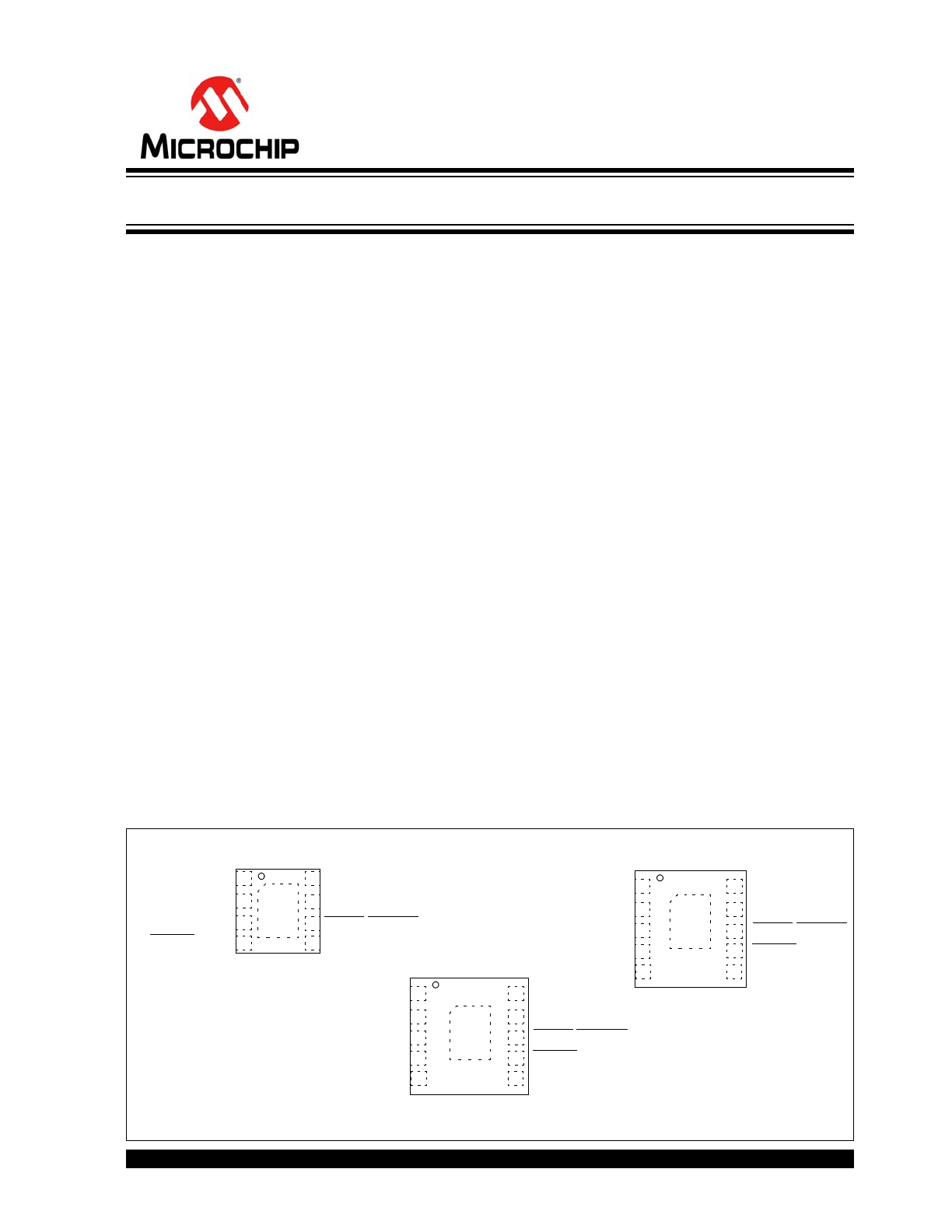
Package Types
1
2
3
4
8
7
6
5
EP
9
V
DD
DP1
DN1
THERM/ADDR
SMCLK
SMDATA
ALERT/THERM2
GND
MCP9902
2 x 2 WDFN*
1
2
3
4
10
9
8
7
EP
11
V
DD
DP1
DN1
DP2
SMCLK
SMDATA
ALERT/THERM2
THERM/ADDR
5
6
DN2
GND
MCP9903
3 x 3 VDFN*
1
2
3
4
10
9
8
7
EP
11
V
DD
DP1
DN1
DP2/DN3
SMCLK
SMDATA
ALERT/THERM2
THERM/ADDR
5
6
DN2/DP3
GND
MCP9904
3 x 3 VDFN*
* Includes Exposed Thermal Pad (EP); see
Table 3-1
.
Multi-Channel Low-Temperature Remote Diode Sensor
MCP9902/3
/4
DS2
0005382C-page 2
2015-20
16 M
ic
rochip
T
e
chnology
In
c.
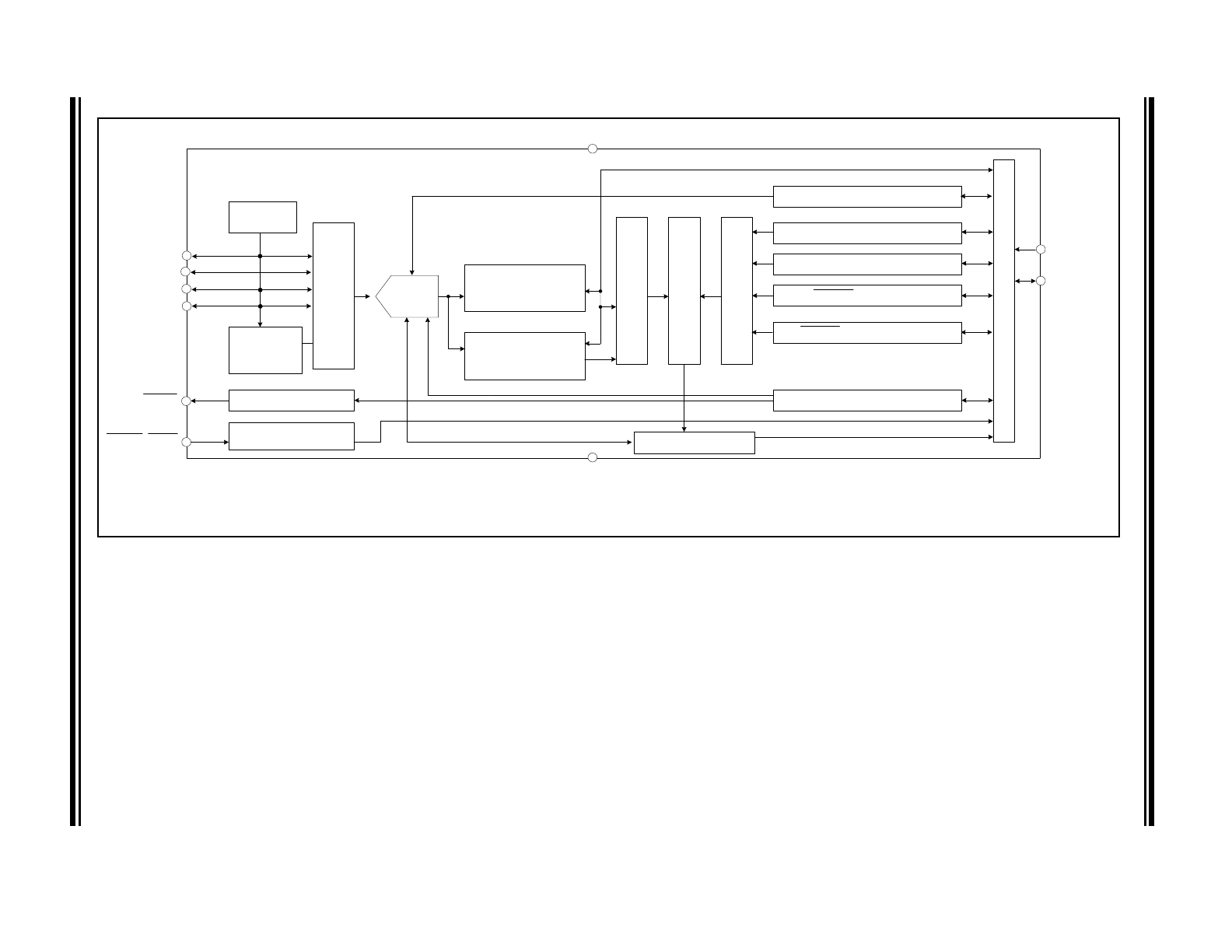
MCP9902/3/4 Functional Block Diagram
Internal
Temp Diode
Switching
Current
Analog
Mux
Internal
Temperature Register
Digital
M
ux
Digital
M
ux
Limit
C
omparator
Low Limit Registers
High Limit Registers
Conversion Rate Register
Interupt Masking
Status Registers
Configuration Register
SMBus
Interface
SMCLK
SMDATA
DP1
DN2
(1)
/DP3
(2)
V
DD
GND
External Temperature
Register(s)
'6 ADC
THERM Limit Register
THERM Hysteresis Register
SMBus Address Decode
ALERT
MCP990X
THERM/ADDR
DN1
DP2
(1)
/DN3
(2)
Note 1:
Second remote channel for MCP9903 and MCP9904.
2:
Third remote channel for MCP9904.
2015-2016 Microchip Technology Inc.
DS20005382C-page 3
MCP9902/3/4
1.0
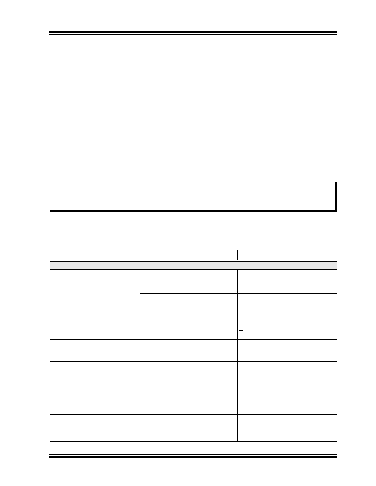
ELECTRICAL CHARACTERISTICS
1.1
Electrical Specifications
Absolute Maximum Ratings
(†)
Ambient Temperature under Bias...................................................................................................... -40°C to +125°C
Storage Temperature ....................................................................................................................... -65°C to +150°C
Voltage on V
DD
with respect to V
SS
................................................................................................... -0.3V to +4.0V
Voltage on all other pins with respect to V
SS
........................................................................... -0.3V to (V
DD
+ 0.3V)
Total Power Dissipation
(
1
)
............................................................................................................................. 500 mW
Maximum Current out of V
SS
pin ..................................................................................................................... 20 mA
Maximum Current into V
DD
pin ........................................................................................................................ 20 mA
Clamp Current, I
K
(V
PIN
< 0 or V
PIN
> V
DD
)
20 mA
ESD Rating, All pins HBM................................................................................................................................. 2000V
Input Current, any pin Except V
DD
10 mA
Note 1:
Power dissipation is calculated as follows: P
DIS
= V
DD
x {I
DD
–
I
OH
} +
{(V
DD
– V
OH
) x I
OH
} +
(V
OL
x I
OL
). Rating up to +85°C.
† NOTICE
: Stresses above those listed under “Absolute Maximum Ratings” may cause permanent damage to the
device. This is a stress rating only and functional operation of the device at those or any other conditions above those
indicated in the operation listings of this specification is not implied. Exposure above maximum rating conditions for
extended periods may affect device reliability.
1.2
DC Characteristics
Electrical Characteristics
: Unless otherwise specified, 3.0 ≤ V
DD
≤ 3.6V at -40°C ≤ T
A
≤ +125°C
Characteristic
Sym.
Min.
Typ.
Max.
Units
Conditions
Power Supply
Supply Voltage
V
DD
3.0
3.3
3.6
V
—
Supply Current
I
DD
—
200
450
µA
0.0625 conversion/second, dynamic
averaging disabled
—
225
600
µA
1 conversion/second, dynamic
averaging enabled
—
450
850
µA
4 conversions/second, dynamic
averaging enabled
—
1120
1500
µA
> 16 conversions/second, dynamic
averaging enabled
One-Shot Supply
Current
I
DD_OS
—
170
230
µA
Device in One-Shot state, no active
SMBus communications, ALERT and
THERM pins not asserted.
Standby Supply Current
I
DD_SBY
—
170
230
µA
Device in Standby state, no SMBus
communications, ALERT and THERM
pins not asserted.
Power-on Reset
Voltage
POR_V
—
0.6
0.9
V
Pin states defined
Power-On Reset
Release Voltage
PORR
—
1.45
—
V
Rising V
DD
Power-Up Timer
t
PWRT
—
10
—
ms
—
V
DD
Rise Rate
V
DD_RISE
0.05
—
—
V/ms
0 to 3V in 60 ms
Supply Voltage
V
DD
3.0
3.3
3.6
V
—
MCP9902/3/4
DS20005382C-page 4
2015-2016 Microchip Technology Inc.
External Temperature Monitor
Temperature Accuracy
(MCP9902)
—
-1
±0.25
+1
°C
-40°C < T
DIODE
< +105°C,
-40°C < T
A
< +65°C
-2
±0.25
+2
°C
-40°C < T
DIODE
< +125°C
-40°C < T
A
< +125°C
Temperature Accuracy
(MCP9903, MCP9904)
—
-1
±0.25
+1
°C
-40°C < T
DIODE
< +125°C,
-40°C < T
A
< +65°C
-2
±0.25
+2
°C
+40°C < T
DIODE
< +125°C
-40°C < T
A
< +125°C
Temperature
Resolution
—
—
0.125
—
°C
—
Internal Temperature Monitor
Temperature Accuracy
—
-1
±0.25
+1
°C
-40°C < T
A
< +65°C
-2
±0.5
+2
°C
-40°C < T
A
< +125°C
Temperature
Resolution
—
—
0.125
—
°C
—
Timing and Capacitive Filter
Time to First
Communications
t
INT_T
—
15
20
ms
Time after power up before ready to
begin communications and
measurement
Conversion Time All
Channels
(MCP9903, MCP9904)
t
CONV
—
190
—
ms
Default settings
Conversion Time All
Channels
(MCP9902)
t
CONV
—
150
—
ms
Default settings
Time to First
Conversion from
Standby
t
CONV1
—
220
—
ms
Default settings
Capacitive Filter
C
FILTER
—
2.2
2.7
nF
Connected across external diode
ALERT and THERM Pins
Output Low Voltage
V
OL
0.4
—
—
V
I
SINK
= 8 mA
Leakage Current
I
LEAK
—
—
±5
µA
ALERT and THERM pins
Device powered or
unpowered
T
A
< +85°C
pull-up voltage < 3.6V
1.2
DC Characteristics (Continued)
Electrical Characteristics
: Unless otherwise specified, 3.0 ≤ V
DD
≤ 3.6V at -40°C ≤ T
A
≤ +125°C
Characteristic
Sym.
Min.
Typ.
Max.
Units
Conditions
1.3
Thermal Specifications
Electrical Characteristics:
Unless otherwise specified, 3.0
V
DD
3.6V at -40C T
A
+125C
Parameters
Sym.
Min.
Typ.
Max.
Units
Test Conditions
Temperature Ranges
Specified Temperature Range
T
A
-40
—
+125
°C
Operating Temperature Range
T
A
-40
—
+125
°C
Storage Temperature Range
T
A
-65
—
+125
°C
Thermal Package Resistances (
Note 1
)
Thermal Resistance, 8L-WDFN, 2x2
JA
—
141.3
—
°C/W
2015-2016 Microchip Technology Inc.
DS20005382C-page 5
MCP9902/3/4
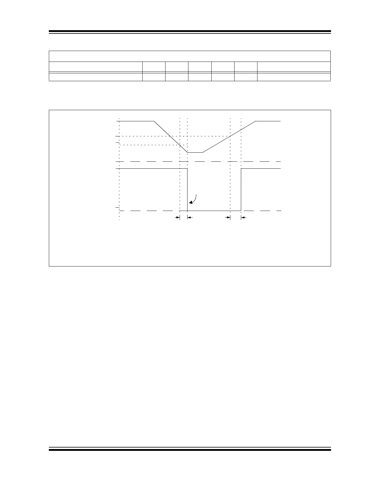
FIGURE 1-1:
POR and POR Rearm With Slow Rising V
DD
.
Thermal Resistance, 10L-VDFN, 3x3
JA
—
78
—
°C/W
Note 1:
JEDEC 2s2p, board size 76.2 x 114.3 x 1.6 mm, 1 via, airflow = 0 m/s.
1.3
Thermal Specifications
Electrical Characteristics:
Unless otherwise specified, 3.0
V
DD
3.6V at -40C T
A
+125C
Parameters
Sym.
Min.
Typ.
Max.
Units
Test Conditions
V
DD
V
POR
V
PORR
V
SS
V
SS
N
POR
T
POR
(
3
)
POR REARM
Note 1:
When N
POR
is low, the device is held in Reset.
2:
T
POR
1
s typical.
3:
T
VLOW
2.7
s typical.
T
VLOW
(
2
)
MCP9902/3/4
DS20005382C-page 6
2015-2016 Microchip Technology Inc.
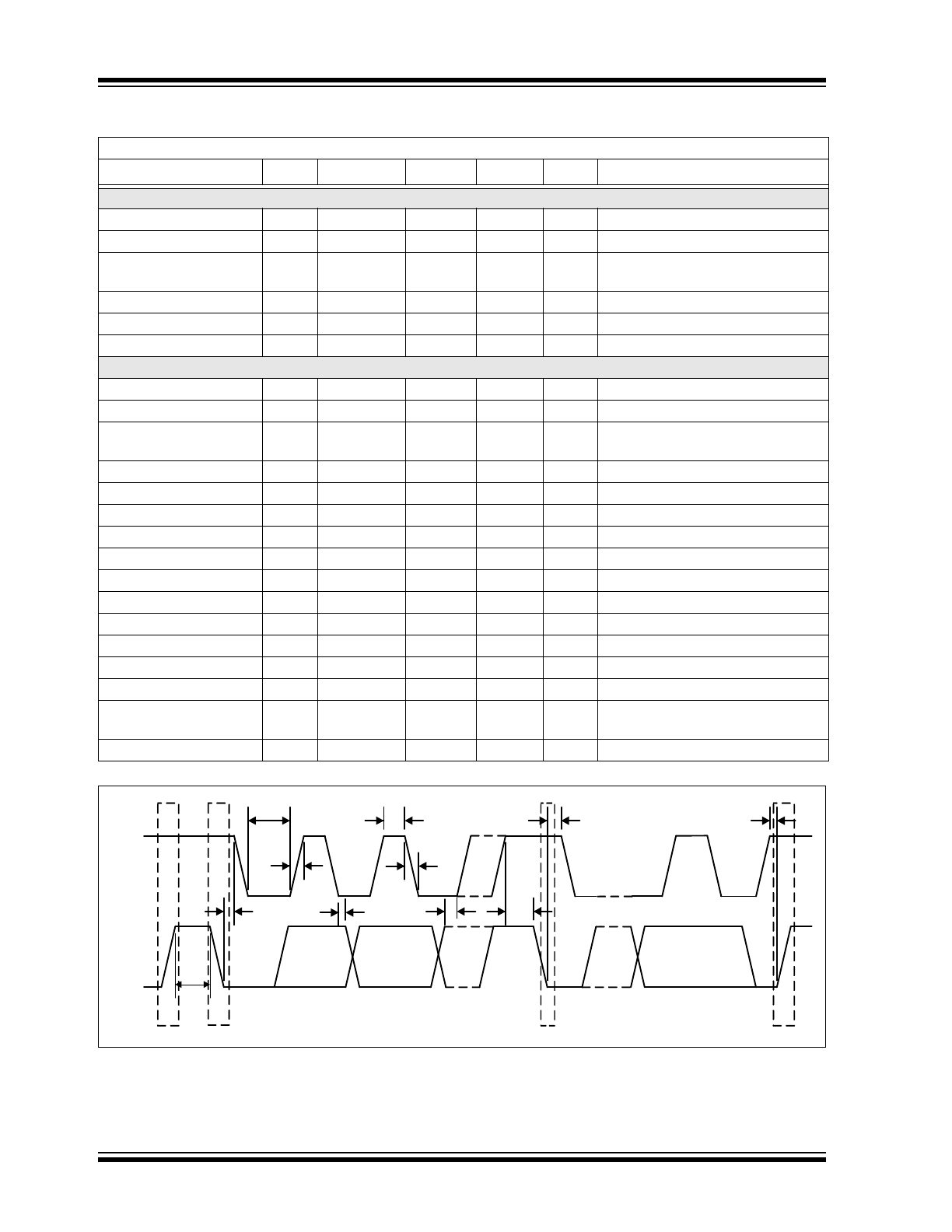
FIGURE 1-2:
SMBus Timing Diagram.
1.4
SMBUS Module Specifications
Operating Conditions
(unless otherwise indicated): 3.0V ≤ V
DD
≤ 3.6V at -40°C ≤ T
A
≤ +85°C
Characteristic
Sym.
Min.
Typ.
Max.
Units
Conditions
SMBus Interface
Input High Voltage
V
IH
2.1
—
V
DD
V
—
Input Low Voltage
V
IL
-0.3
0.8
V
—
Leakage Current
I
LEAK
—
—
±5
µA
Powered or unpowered
T
A
< +85°C
Hysteresis
—
0.1
V
DD
—
mV
—
Input Capacitance
C
IN
—
5
—
pF
—
Output Low Sink Current
I
OL
8.2
—
15
mA
SMDATA = 0.2V
SMBus Timing
Clock Frequency
f
SMB
10
—
400
kHz
—
Spike Suppression
t
SP
—
—
50
ns
—
Bus Free Time Stop to
Start
t
BUF
1.3
—
—
µs
—
Hold Time: Start
t
HD:STA
0.6
—
—
µs
—
Setup Time: Start
t
SU:STA
0.6
—
—
µs
—
Setup Time: Stop
t
SU:STO
0.6
—
—
µs
—
Data Hold Time
t
HD:DAT
0
—
—
µs
—
Data Hold Time
t
HD:DAT
0.3
—
—
µs
When transmitting to the master
Data Setup Time
t
SU:DAT
100
—
—
ns
When receiving from the master
Clock Low Period
t
LOW
1.3
—
—
µs
—
Clock High Period
t
HIGH
0.6
—
—
µs
—
Clock/Data Fall Time
t
FALL
—
—
300
ns
—
Clock/Data Rise Time
t
RISE
—
—
300
ns
Min = 20+0.1 C
LOAD
ns
Capacitive Load
C
LOAD
—
—
400
pF
Min = 20+0.1 C
LOAD
ns
Timeout
t
TIME-
OUT
25
—
35
ms
Per bus line
Clock Frequency
f
SMB
10
—
400
kHz
Disabled by default
SMDATA
SMCLK
T
BUF
P
S
S - Start Condition
P - Stop Condition
P
S
T
HIGH
T
LOW
T
HD:STA
T
SU:STO
T
HD:STA
T
HD:DAT
T
SU:DAT
T
SU:STA
T
FALL
T
RISE
2015-2016 Microchip Technology Inc.
DS20005382C-page 7
MCP9902/3/4
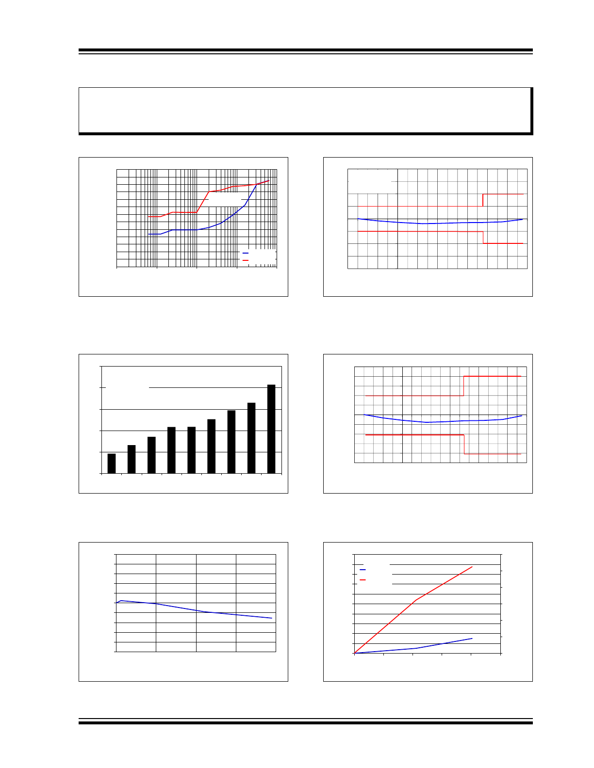
2.0
TYPICAL OPERATING CURVES
Note
: Unless otherwise indicated 3.0
V
DD
3.6V at -40C T
A
+125C.
FIGURE 2-1:
Supply Current vs.
Conversion Rate (T
A
= +25°C, V
DD
= 3.3V).
FIGURE 2-2:
I
DD
vs. Temperature.
FIGURE 2-3:
Temperature Error vs. Filter
Capacitor (V
DD
= 3.3V, T
A
= T
D
= +25°C, 2N3904).
FIGURE 2-4:
Temperature Error vs.
Ambient Temperature (V
DD
= 3.3V, T
D
= +25°C,
16 Units, 2N3904).
FIGURE 2-5:
Temperature Error vs.
Remote Temperature. (V
DD
= 3.3V, T
D
= +25°C,
16 Units, 2N3904).
FIGURE 2-6:
Temperature Error vs.
Series Resistance (T
A
= +25°C, V
DD
= 3.3V).
Note:
The graphs and tables provided following this note are a statistical summary based on a limited number of
samples and are provided for informational purposes only. The performance characteristics listed herein
are not tested or guaranteed. In some graphs or tables, the data presented may be outside the specified
operating range (e.g., outside specified power supply range) and therefore outside the warranted range.
0
100
200
300
400
500
600
700
800
900
1000
1100
1200
1300
0.01
0.1
1
10
100
Supply
Current
(µA)
Conversion Rate (Hz)
Disabled
Enabled
Dynamic
Averaging
0
50
100
150
200
250
-40C -20C
0C
25C
45C
65C
85C 105C 125C
Average of 5
devices
-0.25
-0.2
-0.15
-0.1
-0.05
0
0.05
0.1
0.15
0.2
0.25
0
1000
2000
3000
4000
T
emperature Error (
°C)
Filter Capacitance (pF)
-4
-3
-2
-1
0
1
2
3
4
-50
-40
-30
-20
-10
0
10
20
30
40
50
60
70
80
90
100
110
120
130
T
e
meprature Error (°C)
Temperature (°C)
V
DD
= 3.3V
T
D
= 25°C
30 Units
-2.5
-2
-1.5
-1
-0.5
0
0.5
1
1.5
2
2.5
-50
-40
-30
-20
-10
0
10
20
30
40
50
60
70
80
90
100
110
120
130
T
e
meprature Error (°C)
Temperature (°C)
0
20
40
60
80
100
120
0
0.1
0.2
0.3
0.4
0.5
0.6
0.7
0.8
0.9
1
0
50
100
150
200
250
T
emperaure Error
(°
C)
T
emperature Error (
°C)
Series Resistance (Ω)
Disabled
Enabled
REC

MCP9902/3/4
DS20005382C-page 8
2015-2016 Microchip Technology Inc.
3.0
PIN DESCRIPTIONS
The MCP9902/3/4 has two variants that include
features unique to each device. Refer to the table to
determine applicability of the pin descriptions.
The description of the pins is listed in
Table 3-1
.
3.1
Power Supply (V
DD
)
This pin is used to supply power to the device.
3.2
Diode 1 Pair (DN1/DP1)
Remote Diode 1 anode (DP1) and cathode (DN1) pins
for the MCP9902/3/4.
3.3
Diode 2 Pair (DN2/DP2)
Remote Diode 2 anode (DP2) and cathode (DN2) pins
for the MCP9903.
3.4
Anti-Parallel Diode Pair (DN3/DP2
and DN2/DP3) (MCP9904 only)
• DP2/DN3: DP2 anode and DN3 cathode
• DN2/DP3: DN2 cathode and DP3 anode
3.5
THERM LIMIT ALERT
(THERM/ADDR)
This pin asserts low when the hardware-set THERM
limit threshold is exceeded by one of the temperature
sensors. The assertion of this signal can’t be controlled
or masked by register setting. If enabled, the SMBus
slave address is set by the pull-up resistor on this pin.
3.6
Ground (GND)
This pin is used for system ground for the device.
3.7
Maskable ALERT
(ALERT/THERM2)
This pin asserts when a diode temperature exceeds
the ALERT threshold. This pin may be masked by
register settings.
3.8
SMBus Data (SMDATA)
This is the open drain, bidirectional data pin for SMBus
communication.
3.9
SMBus Clock (SMCLK)
This is the SMBus input clock pin for SMBus
communication.
3.10
Exposed Thermal Pad (EP)
Not internally connected, but recommend grounding for
mechanical support.
TABLE 3-1:
PIN FUNCTION TABLE
MCP9902
WDFN
MCP9903
VDFN
MCP9904
VDFN
Pin
Name
Pin
Type
Description
1
1
1
V
DD
P
Power
2
2
2
DP1
Analog
Diode 1/2 Connection
3
3
3
DN1
Analog
Diode 1/2 Connection
—
4
4
DP2
(
1
)
(/DN3)
(
2
)
Analog
Diode 1/2 Connection
—
5
5
DN2
(
1
)
(/DP3)
(
2
)
Analog
Diode 1/2 Connection
5
6
6
GND
P
Ground
4
7
7
THERM/ADDR
OD
Non-Maskable THERM
6
8
8
ALERT/THERM2
OD
Maskable ALERT/THERM2
7
9
9
SMDATA
OD
SMBus Clock
8
10
10
SMCLK
OD
SMBus Data
9
11
11
EP
—
Exposed Thermal pad
Note 1:
MCP9903 only.
2:
MCP9904 only.
3:
See
Section 3.10 “Exposed Thermal Pad (EP)”
for grounding recommendations.
2015-2016 Microchip Technology Inc.
DS20005382C-page 9
MCP9902/3/4
4.0
FUNCTIONAL DESCRIPTION
Thermal management is performed in cooperation
with a host device. This consists of the host reading
the temperature data of both the external and internal
temperature diodes of the MCP9902/3/4 and using
that data to control the speed of one or more fans.
The MCP9902/3/4 has two levels of monitoring. The
first provides a maskable ALERT signal to the host
when the measured temperatures exceed user pro-
grammable limits. This allows the MCP9902/3/4 to be
used as an independent thermal watchdog to warn the
host of temperature hot spots without direct control by
the host. The second level of monitoring provides a
non-maskable interrupt on the THERM output if the
measured temperatures meet or exceed a second pro-
grammable limit.
Figure 4-1
shows a system level block diagram of the
MCP9902/3/4.
FIGURE 4-1:
MCP9902/3/4
System
Diagram.
4.1
Power States
The MCP9902/3/4 has two modes of operation:
• Active (Run) - In this mode of operation, the ADC
is converting on all temperature channels at the
programmed conversion rate. The temperature
data is updated at the end of every conversion
and the limits are checked. In Active mode, writing
to the one-shot register will do nothing.
• Standby (Stop) - In this mode of operation, the
majority of circuitry is powered down to reduce
supply current. The temperature data is not
updated and the limits are not checked. In this
mode of operation, the SMBus is fully active and
the part will return requested data. Writing to the
one-shot register will enable the device to update
all temperature channels. Once all the channels
are updated, the device will return to the Standby
mode.
4.2
Conversion Rates
The MCP9902/3/4 may be configured for different con-
version rates based on the system requirements. The
default conversion rate is 4 conversions per second.
Other available conversion rates are shown in
Table 4-1
.
4.3
Dynamic Averaging
Dynamic averaging allows the MCP9902/3/4 to
measure the external diode channel for an extended
time based on the selected conversion rate. This
functionality can be disabled for increased power
savings at the lower conversion rates (see
Register 5-6
). When dynamic averaging is enabled,
the device will automatically adjust the sampling and
measurement time for the external diode channels.
This allows the device to average 2x or 16x longer
than the normal 11 bit operation (nominally 21 ms per
channel) while still maintaining the selected
conversion rate. The benefits of dynamic averaging
are improved noise rejection due to the longer
integration time as well as less random variation of the
temperature measurement.
When enabled, the dynamic averaging applies when a
one-shot command is issued. The device will perform
the desired averaging during the one-shot operation
according to the selected conversion rate.
When enabled, the dynamic averaging will affect the
typical supply current based on the chosen conversion
rate as shown in the power supply characteristics in
Table 1.2 "DC Characteristics"
.
CPU/GPU
MCP990X
Host
DP1
DN1
SMDATA
Thermal
Junction
SMCLK
SMBus
Interface
THERM/ADDR
ALERT
Power
Control
V
DD
GND
V
DD
= 3.3V
3.3V – 5V
DN2/
DP3
DP2/
DN3
Optional
Anti-parallel
diode
MCP9903/4 only
TABLE 4-1:
CONVERSION RATE
CONV<3:0>
Conversions/
Second
HEX
3
2
1
0
0h
0
0
0
0
1/16
1h
0
0
0
1
1/8
2h
0
0
1
0
1/4
3h
0
0
1
1
1/2
4h
0
1
0
0
1
5h
0
1
0
1
2
6h
0
1
1
0
4 (default)
7h
0
1
1
1
8
8h
1
0
0
0
16
9h
1
0
0
1
32
Ah
1
0
1
0
64
Bh - Fh
All others
1
MCP9902/3/4
DS20005382C-page 10
2015-2016 Microchip Technology Inc.
4.4
THERM Output
The THERM output is asserted independently of the
ALERT output and cannot be masked. Whenever any
of the measured temperatures exceed the user
programmed Therm Limit values for the programmed
number of consecutive measurements, the THERM
output is asserted. Once it has been asserted, it will
remain asserted until all measured temperatures drop
below the Therm Limit minus the Therm Hysteresis
(also programmable).
When the THERM output is asserted, the THERM
status bits will likewise be set. Reading these bits will
not clear them until the THERM output is deasserted.
Once the THERM output is deasserted, the THERM
status bits will be automatically cleared.
4.5
THERM Pin Address Decoding
The Address decode is performed by pulling known
currents from V
DD
through the external resistor
causing the pin voltage to drop based on the
respective current/resistor relationship. This pin
voltage is compared against a threshold that
determines the value of the pull-up resistor.
The MCP9902/3/4-A SMBus slave address is deter-
mined by the pull-up resistor on the THERM/ADDR pin
as shown in
Table 4-2
.
The MCP9902-1 I
2
C/SMBus address is hard coded to
1001_100(r/w).
The MCP9902-2 I
2
C/SMBus address is hard coded to
1001_101(r/w).
The MCP9903-1 I
2
C/SMBus address is hard coded to
1001_100(r/w).
The MCP9903-2 I
2
C/SMBus address is hard coded to
1001_101(r/w).
The MCP9904-1 I
2
C/SMBus address is hard coded to
1001_100(r/w).
The MCP9904-2 I
2
C/SMBus address is hard coded to
1001_101(r/w).
4.6
ALERT/THERM2 Output
4.6.1
ALERT/THERM2 PIN INTERRUPT
MODE
When configured to operate in interrupt mode, the
ALERT/THERM2 pin asserts low when an out-of-limit
measurement (> high limit or < low limit) is detected on
any diode or when an external diode fault is detected.
The ALERT/THERM2 pin will remain asserted as long
as an out-of-limit condition remains. Once the
out-of-limit condition has been removed, the
ALERT/THERM2 pin will remain asserted until the
appropriate status bits are cleared.
The ALERT/THERM2 pin can be masked by setting
the MASK_ALL bit. Once the ALERT/THERM2 pin has
been masked, it will be deasserted and remain deas-
serted until the MASK_ALL bit is cleared by the user.
Any interrupt conditions that occur while the
ALERT/THERM2 pin is masked will update the Status
Register normally. There are also individual channel
masks (see
Register 5-20
).
The ALERT/THERM2 pin is used as an interrupt signal
or as an SMBus Alert signal that allows an SMBus
slave to communicate an error condition to the master.
One or more ALERT/THERM2 Outputs can be
hard-wired together.
4.6.2
ALERT/THERM2 PIN IN THERM
MODE
When the ALERT/THERM2 pin is configured to oper-
ate in THERM mode, it will be asserted if any of the
measured temperatures exceeds the respective high
limit. The ALERT/THERM2 pin will remain asserted
until all temperatures drop below the corresponding
high limit minus the Therm Hysteresis value.
When the ALERT/THERM2 pin is asserted in THERM
mode, the corresponding high limit status bits will be
set. Reading these bits will not clear them until the
ALERT/THERM2 pin is deasserted. Once the
ALERT/THERM2 pin is deasserted, the status bits will
be automatically cleared.
The MASK_ALL bit will not block the ALERT/THERM2
pin in this mode; however, the individual channel
masks (see
Register 5-20
) will prevent the respective
channel from asserting the ALERT/THERM2 pin.
4.6.3
DEFAULT POWER UP CONDITIONS
On power-up, the ALERT/THERM2 is disabled and the
MASK ALL (MSKAL) bit in the CONFIG register (see
Register 5-6
) is set. Additionally, an artificial fault has
been placed in the device, and is enabled at power up.
The FAULT TEST (FT_TST) bit in the Fault Status reg-
ister (see
Register 5-20
) will allow the assertion of the
ALERT/THERM2 pin when this test mode is enabled
once MSKAL is cleared. To use the ALERT/THERM2
functions described in this section, the MSKAL bit must
be set to ‘0’, and the FT_TST bit to ‘1’ in order for the
pin to function properly.
TABLE 4-2:
I
2
C/SMBUS ADDRESS
DECODE
Pull Up Resistor on
THERM pin (±5%)
SMBus Address
4.7 kΩ
1111_100 (r/w)b
6.8 kΩ
1011_100 (r/w)b
10 kΩ
1001_100 (r/w)b
15 kΩ
1101_100 (r/w)b
22 kΩ
0011_100 (r/w)b
33 kΩ
0111_100 (r/w)b