
2013 Microchip Technology Inc.
DS20005192B-page 1
MCP9844
Features:
• 1MHz, 2-Wire I
2
C™ Interface
• User-Selectable Measurement Resolution:
- +0.5°C, +0.25°C, +0.125°C, +0.0625°C
• User-Programmable Temperature Limits:
- Temperature Window Limit
- Critical Temperature Limit
• User-Programmable Temperature Alert Output
• Specified V
DD
Range: 1.7V to 3.6V
• Operating Current: 100 µA (typical)
• Available Package: 8-Pin TDFN
Temperature Sensor Features:
• Temperature-to-Digital Converter (°C)
• Sensor Accuracy:
- ±0.2°C/±1°C (typ./max.)
+75°C to +95°C
- ±0.5°C/±2°C (typ./max.)
+40°C to +125°C
- ±1°C/±3°C (typ./max.)
-40°C to +125°C
Typical Applications:
• Temperature Sensing for Solid State Drive (SSD)
• General Purpose Temperature Datalog
• General Purpose
• Industrial Applications
• Industrial Freezers and Refrigerators
• Food Processing
• Personal Computers and Servers
• PC Peripherals
• Consumer Electronics
• Handheld/Portable Devices
Description:
Microchip Technology Inc.’s MCP9844 digital
temperature sensor converts temperature from -40°C
to +125°C to a digital word. It provides an accuracy of
±0.2°C/±1°C (typical/maximum) from +75°C to +95°C
with an operating voltage of 1.7V to 3.6V.
The MCP9844 digital temperature sensor comes with
user-programmable registers that provide flexibility for
temperature sensing applications. The registers allow
user-selectable settings such as Shutdown or Low-
Power modes, and the specification of temperature
event boundaries. When the temperature changes
beyond the specified event boundary limits, the
MCP9844 outputs an Alert signal at the Event pin. The
user has the option of setting the temperature event
output signal polarity as either an active-low or active-
high comparator output for the thermostat operation, or
as a temperature event interrupt output for
microprocessor-based systems.
This sensor has an industry standard I
2
C Fast Mode
Plus compatible 1 MHz serial interface.
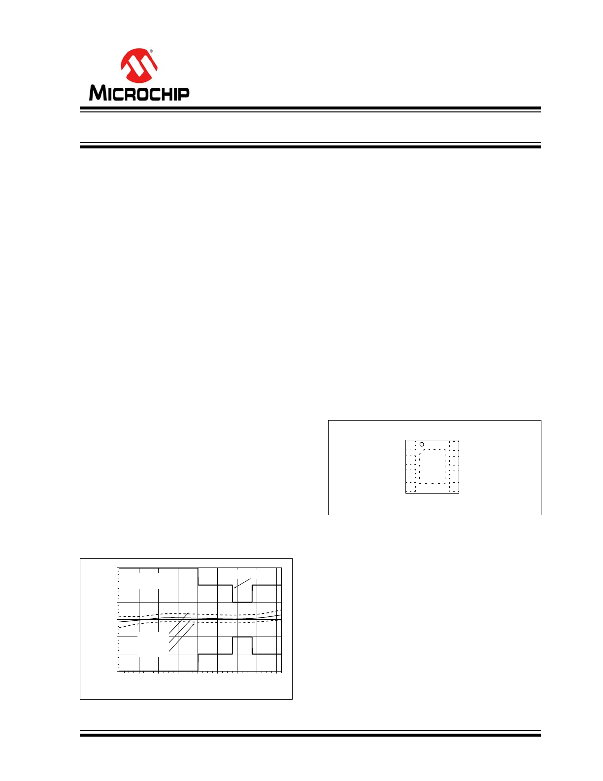
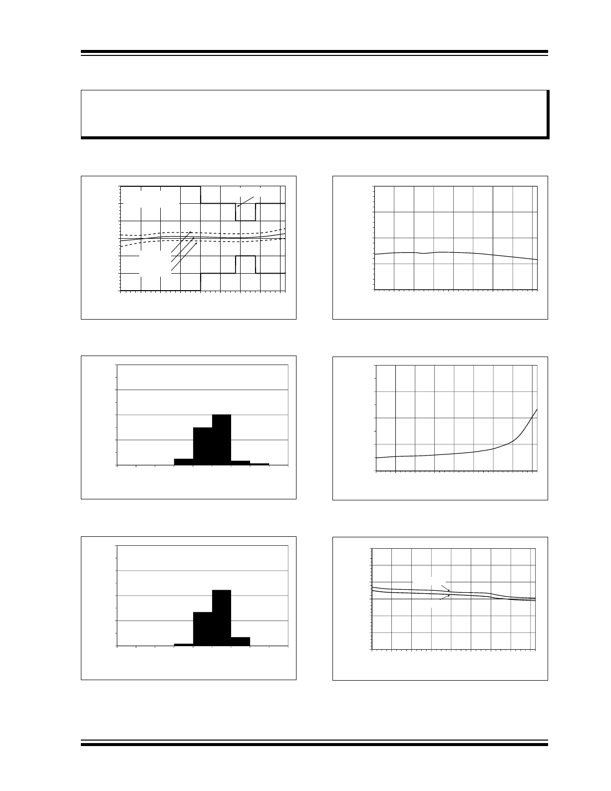
Package Types
-3.0
-2.0
-1.0
0.0
1.0
2.0
3.0
-40
-20
0
20
40
60
80
100
120
T
e
mperature Accuracy
(°C)
T
A
(°C)
V
DD
= 1.7 V to 3.6 V
16 units
Spec. Limits
+Std. Dev.
Average
-Std. Dev.
8-Pin 2x3 TDFN *
* Includes Exposed Thermal Pad (EP); see
Table 3-1
.
SCL
Event
SDA
A1
A2
1
2
3
4
8
7
6
5
GND
A0
V
DD
EP
9
±1°C Accurate, 1.8V Digital Temperature Sensor
MCP9844
DS20005192B-page 2
2013 Microchip Technology Inc.
1.0
ELECTRICAL
CHARACTERISTICS
Absolute Maximum Ratings †
V
DD
.................................................................................. 4.0V
Voltage at all Input/Output pins ............... GND – 0.3V to 4.0V
Pin A0....................................................... GND – 0.3V to 11V
Storage temperature .....................................-65°C to +150°C
Ambient temp. with power applied ................-40°C to +125°C
Junction Temperature (T
J
)...........................................+150°C
ESD protection on all pins (HBM:MM) ................. (4 kV:200V)
Latch-Up Current at each pin (25°C)........................ ±200 mA
†Notice:
Stresses above those listed under “Maximum
ratings” may cause permanent damage to the device. This is
a stress rating only and functional operation of the device at
those or any other conditions above those indicated in the
operational listings of this specification is not implied.
Exposure to maximum rating conditions for extended periods
may affect device reliability.
TEMPERATURE SENSOR DC CHARACTERISTICS
Electrical Specifications:
Unless otherwise indicated, V
DD
= 1.7V to 3.6V, GND = Ground,
and T
A
= -40°C to +125°C.
Parameters
Sym.
Min.
Typ.
Max.
Unit
Conditions
Temperature Sensor Accuracy
+75°C < T
A
+95°C
T
ACY
-1.0
±0.2
+1.0
°C
V
DD
= 1.8V
+40°C < T
A
+125°C
-2.0
±0.5
+2.0
°C
-40°C < T
A
+125°C
-3.0
±1
+3.0
°C
Temperature Conversion Time
0.5°C/bit
t
CONV
—
30
—
ms
0.25°C/bit (POR default)
—
65
125
ms 15 s/sec (typical) (See Section
5.2.4
)
0.125°C/bit
—
130
—
ms
0.0625°C/bit
—
260
—
ms
Power Supply
Specified Voltage Range
V
DD
1.7
—
3.6
V
Operating Current
I
DD
—
100
500
µA
Shutdown Current
I
SHDN
—
0.2
1
µA
T
A
= 85°C
Power On Reset (POR)
V
POR
—
1.4
1.6
V
Threshold for falling V
DD
voltage
Settling time after POR
t
POR
—
—
1
ms For warm and cold power cycles
Line Regulation
°C
—
0.2
—
°C
V
DD
= 1.7V to 3.6V
Event Output (Open-Drain output, external pull-up resistor required), see Section
5.2.3
High-level Current (leakage)
I
OH
—
—
1
µA
V
OH
= V
DD
Low-level Voltage
V
OL
—
—
0.4
V
I
OL
= 3 mA (Active-Low, Pull-up
Resistor)
Thermal Response, from +25°C (Air) to +125°C (oil bath)
TDFN-8
t
RES
—
0.7
—
s
Time to 63% (89°C)
2013 Microchip Technology Inc.
DS20005192B-page 3
MCP9844
INPUT/OUTPUT PIN DC CHARACTERISTICS
Electrical Specifications:
Unless otherwise indicated, V
DD
= 1.7V to 3.6V, GND = Ground and
T
A
= -40°C to +125°C.
Parameters
Sym.
Min.
Typ.
Max.
Units
Conditions
Serial Input/Output (SCL, SDA, A0, A1, A2)
Input
High-level Voltage
V
IH
0.7V
DD
—
—
V
Low-level Voltage
V
IL
—
—
0.3V
DD
V
Input Current
I
IN
—
—
±5
µA
SDA and SCL only
Input Impedance (A0, A1, A2)
Z
IN
—
1
—
M
V
IN
> V
IH
Input Impedance (A0, A1, A2)
Z
IN
—
200
—
k
V
IN
< V
IL
Output (SDA only)
Low-level Voltage
V
OL
—
—
0.4
V
I
OL
= 3 mA
High-level Current (leakage)
I
OH
—
—
1
µA
V
OH
= V
DD
Low-level Current
I
OL
20
—
—
mA
V
OL
= 0.4V, V
DD
≥ 2.2V
6
—
—
mA
V
OL
= 0.6V
Capacitance
C
IN
—
5
—
pF
SDA and SCL Inputs
Hysteresis
V
HYST
—
0.05V
DD
—
V
Spike Suppression
T
SP
—
—
50
ns
TEMPERATURE CHARACTERISTICS
Electrical Specifications:
Unless otherwise indicated, V
DD
= 1.7V to 3.6V, GND = Ground,
and T
A
= -40°C to +125°C.
Parameters
Sym.
Min.
Typ.
Max.
Units
Conditions
Temperature Ranges
Specified Temperature Range
T
A
-40
—
+125
°C
Note 1
Operating Temperature Range
T
A
-40
—
+125
°C
Storage Temperature Range
T
A
-65
—
+150
°C
Thermal Package Resistances
Thermal Resistance, 8L-TDFN
JA
—
52.5
—
°C/W
Note 1:
Operation in this range must not cause T
J
to exceed Maximum Junction Temperature (+150°C).
MCP9844
DS20005192B-page 4
2013 Microchip Technology Inc.
TIMING DIAGRAM
SERIAL INTERFACE TIMING SPECIFICATIONS
Electrical Specifications:
Unless otherwise indicated, GND = Ground, T
A
= -40°C to +125°C, and C
L
= 80 pF
Note 1
.
V
DD
= 1.7V to 3.6V
V
DD
= 2.2V to 3.6V
100 kHz
400 kHz
1000 kHz
Parameters
Sym.
Min.
Max.
Min.
Max.
Min.
Max.
Units
2-Wire I
2
C™ Interface
Serial port frequency (
Note 2
,
4
)
f
SCL
10
100
10
400
10
1000
kHz
Low Clock (
Note 2
)
t
LOW
4700
—
1300
—
500
—
ns
High Clock
t
HIGH
4000
—
600
—
260
—
ns
Rise time
(
Note 5
)
t
R
—
1000
20
300
—
120
ns
Fall time (
Note 5
)
t
F
20
300
20
300
—
120
ns
Data in Setup time (
Note 3
)
t
SU:DAT
250
—
100
—
50
—
ns
Data in Hold time (
Note 6
)
t
HD:DI
0
—
0
—
0
—
ns
Data out Hold time (
Note 4
)
t
HD:DO
200
900
200
900
0
350
ns
Start Condition Setup time
t
SU:STA
4700
—
600
—
260
—
ns
Start Condition Hold time
t
HD:STA
4000
—
600
—
260
—
ns
Stop Condition Setup time
t
SU:STO
4000
—
600
—
260
—
ns
Bus Idle/Free
t
B-FREE
4700
—
1300
—
500
—
ns
Time out
t
OUT
25
35
25
35
25
35
ms
Bus Capacitive load
C
b
—
—
—
400
—
100
pf
Note 1:
All values referred to V
IL MAX
and V
IH MIN
levels.
2:
If t
LOW
> t
OUT
, the temperature sensor I
2
C interface will time out. A Repeat Start command is required for
communication.
3:
This device can be used in a Standard mode I
2
C bus system, but the requirement t
SU:DAT
250 ns must
be met. This device does not stretch SCL Low period. It outputs the next data bit to the SDA line within t
R
MAX
+ t
SU:DAT MIN
= 1000 ns + 250 ns = 1250 ns (according to the Standard mode I
2
C bus specification)
before the SCL line is released.
4:
As a transmitter, the device provides internal minimum delay time t
HD:DAT MIN
to bridge the undefined
region (min. 200 ns) of the falling edge of SCL t
F MAX
to avoid unintended generation of Start or Stop
conditions.
5:
Characterized but not production tested.
6:
As a receiver, SDA should not be sampled at the falling edge of SCL. SDA can transition t
HD:DI
0 ns after
SCL toggles Low.
t
SU:
ST
O
t
SU
:D
I
t
SU
:D
I
t
SU
:S
TO
t
B:
FR
EE
SCL
SDA
t
HD
:D
I
/ t
HD
:DO
t
HI
GH
t
LOW
t
OU
T
t
R
, t
F
Start Condition
Data Transmission
Stop Condition
2013 Microchip Technology Inc.
DS20005192B-page 5
MCP9844
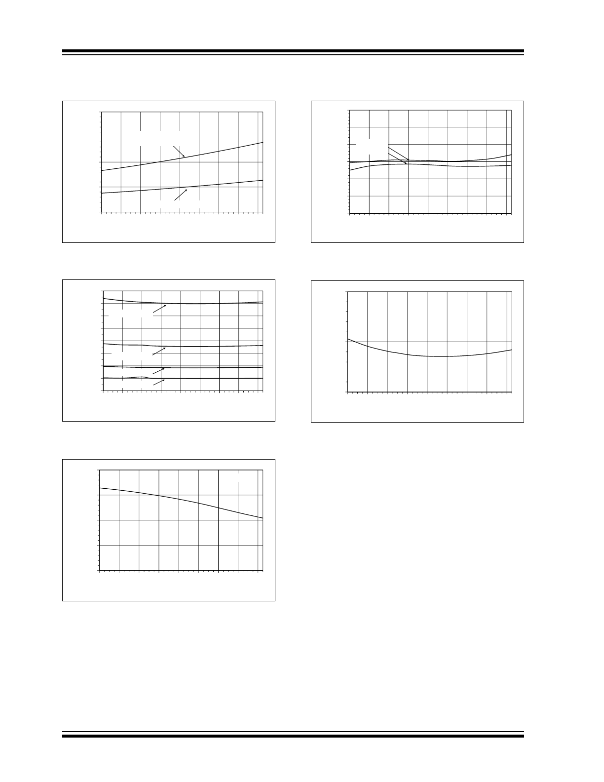
2.0
TYPICAL PERFORMANCE CURVES
Note:
Unless otherwise indicated, V
DD
= 1.7V to 3.6V, GND = Ground, SDA/SCL pulled-up to V
DD
, and
T
A
= -40°C to +125°C.
FIGURE 2-1:
Temperature Accuracy.
FIGURE 2-2:
Temperature Accuracy
Histogram, T
A
= + 85 °C.
FIGURE 2-3:
Temperature Accuracy
Histogram, T
A
= + 25 °C.
FIGURE 2-4:
Supply Current Vs.
Temperature.
FIGURE 2-5:
Shutdown Current Vs.
Temperature.
FIGURE 2-6:
Power-On Reset Threshold
Voltage Vs. Temperature.
Note:
The graphs and tables provided following this note are a statistical summary based on a limited number of
samples and are provided for informational purposes only. The performance characteristics listed herein
are not tested or guaranteed. In some graphs or tables, the data presented may be outside the specified
operating range (e.g., outside specified power supply range) and therefore outside the warranted range.
-3.0
-2.0
-1.0
0.0
1.0
2.0
3.0
-40
-20
0
20
40
60
80
100
120
T
e
mperature Accuracy
(°C)
T
A
(°C)
V
DD
= 1.7 V to 3.6 V
16 units
Spec. Limits
+Std. Dev.
Average
-Std. Dev.
25%
50%
75%
100%
Occurrences
T
A
= +85 °C
V
DD
= 1.7 V - 3.6 V
16 units
0%
-1.00
-0.75
-0.50
-0.25
0.00
0.25
0.50
0.75
1.00
Temperature Accuracy (°C)
25%
50%
75%
100%
Occurrences
T
A
= +25 °C
V
DD
= 1.7 V - 3.6 V
16 units
0%
-1.00
-0.75
-0.50
-0.25
0.00
0.25
0.50
0.75
1.00
Temperature Accuracy (°C)
75
100
125
150
I
DD
(µA)
50
75
-40
-20
0
20
40
60
80
100
120
T
A
(°C)
0 25
0.50
0.75
1.00
I
SHDN
(µA)
0.00
0.25
-40
-20
0
20
40
60
80
100
120
T
A
(°C )
1
1.2
1.4
1.6
1.8
V
PO
R
(V)
Falling V
DD
Rising V
DD
0.6
0.8
-40
-20
0
20
40
60
80
100
120
T
A
(°C)
MCP9844
DS20005192B-page 6
2013 Microchip Technology Inc.
Note:
Unless otherwise indicated, V
DD
= 1.7V to 3.6V, GND = Ground, SDA/SCL pulled-up to V
DD
, and
T
A
= -40°C to +125°C.
FIGURE 2-7:
Event Output and SDA V
OL
Vs. Temperature.
FIGURE 2-8:
Temperature Conversion
Rate Vs. Temperature.
FIGURE 2-9:
SDA I
OL
Vs. Temperature.
FIGURE 2-10:
Line Regulation: Change in
Temperature Accuracy Vs. Change in V
DD
.
FIGURE 2-11:
I
2
C™ Protocol Time-out Vs.
Temperature.
0 1
0.2
0.3
0.4
e
nt & SDA
V
OL
(V)
SDA, I
OL
= 20 mA
V
DD
= 2.2 V to 3.6 V
0
0.1
-40
-20
0
20
40
60
80
100
120
Ev
e
T
A
(°C)
Event, I
OL
= 3 mA
50
75
100
125
150
175
200
t
CONV
(ms)
0.0625 °C/LSb
0.125 °C/LSb
0
25
50
-40
-20
0
20
40
60
80
100
120
T
A
(°C)
0.25 °C/LSb
0.5 °C/LSb
20
30
40
50
SDA
I
OL
(mA)
V
OL
= 0.6V
10
20
-40
-20
0
20
40
60
80
100
120
T
A
(°C)
-1.0
0.0
1.0
2.0
3.0
lized T
e
mp. Error (°C)
V
DD
= 1.7 V
V
DD
= 3.6 V
-3.0
-2.0
-40
-20
0
20
40
60
80
100
120
Norma
l
T
A
(°C)
30
35
C
Bus t
OUT
(ms)
25
-40
-20
0
20
40
60
80
100
120
I
2
C
T
A
(°C)
2013 Microchip Technology Inc.
DS20005192B-page 7
MCP9844
3.0
PIN DESCRIPTION
The descriptions of the pins are listed in
Table 3-1
.
TABLE 3-1:
PIN FUNCTION TABLES
3.1
Address Pins (A0, A1, A2)
These pins are device address input pins.
The address pins correspond to the Least Significant
bits (LSb) of the address bits. The Most Significant bits
(MSb) are A6, A5, A4, A3. Refer to
Table 3-2
.
All address pins have an internal pull-down resistor.
3.2
Ground Pin (GND)
The GND pin is the system ground pin.
3.3
Serial Data Line (SDA)
The SDA is a bidirectional input/output pin used to
serially transmit data to/from the host controller. This
pin requires a pull-up resistor. (See
Section 4.0
“Serial Communication”
.)
3.4
Serial Clock Line (SCL)
The SCL is a clock input pin. All communication and
timing is relative to the signal on this pin. The clock is
generated by the host or master controller on the bus.
(See
Section 4.0 “Serial Communication”
.)
3.5
Temperature Alert, Open-Drain
Output (Event)
The MCP9844 temperature Event output pin is an
open-drain output. The device outputs a signal when
the ambient temperature goes beyond the user
programmed temperature limit. (See
Section 5.2.3
“Event Output Configuration”
.)
3.6
Power Pin (V
DD
)
V
DD
is the power pin. The operating voltage range, as
specified in the DC electrical specification table, is
applied on this pin.
3.7
Exposed Thermal Pad (EP)
There is an internal electrical connection between the
Exposed Thermal Pad (EP) and the GND pin; they can
be connected to the same potential on the Printed
Circuit Board (PCB). This provides better thermal
conduction from the PCB to the die.
MCP9844
Symbol
Description
TDFN
1
A0
Slave Address
2
A1
Slave Address
3
A2
Slave Address
4
GND
Ground
5
SDA
Serial Data Line
6
SCL
Serial Clock Line
7
Event
Temperature Alert Output
8
V
DD
Power Pin
9
EP
Exposed Thermal Pad (EP); can be connected to GND.
TABLE 3-2:
MCP9844 ADDRESS BYTE
Device
Address Code
Slave
Address
A6
A5
A4
A3
A2
A1
A0
Sensor
0
0
1
1
X
1
X
1
X
1
Note 1:
User-selectable address is shown by X,
where X is ‘1’ or ‘0’ for V
DD
and GND,
respectively
MCP9844
DS20005192B-page 8
2013 Microchip Technology Inc.
4.0
SERIAL COMMUNICATION
4.1
2-Wire Standard Mode I
2
C™
Protocol-Compatible Interface
The MCP9844 serial clock input (SCL) and the
bidirectional serial data line (SDA) form a 2-wire
bidirectional Standard mode I
2
C compatible
communication port (refer to the
Input/Output Pin DC
Characteristics
table and the
Serial Interface Timing
Specifications
table).
The following MCP9844 bus protocol is defined in
Table 4-1
.
TABLE 4-1:
MCP9844 SERIAL BUS
PROTOCOL DESCRIPTIONS
4.1.1
DATA TRANSFER
Data transfers are initiated by a Start condition
(START), followed by a 7-bit device address and a
read/write bit. An Acknowledge (ACK) from the slave
confirms the reception of each byte. Each access must
be terminated by a Stop condition (STOP).
Repeated communication is initiated after t
B-FREE
.
This device does not support sequential register read/
write. Each register needs to be addressed using the
Register Pointer.
This device supports the Receive Protocol. The
register can be specified using the pointer for the initial
read. Each repeated read or receive begins with a Start
condition and address byte. The MCP9844 retains the
previously selected register. Therefore, they output
data from the previously specified register (repeated
pointer specification is not necessary).
4.1.2
MASTER/SLAVE
The bus is controlled by a master device (typically a
microcontroller) that controls the bus access and
generates the Start and Stop conditions. The MCP9844
is a slave device and does not control other devices in
the bus. Both master and slave devices can operate as
either transmitter or receiver. However, the master
device determines which mode is activated.
4.1.3
START/STOP CONDITION
A high-to-low transition of the SDA line (while SCL is
high) is the Start condition. All data transfers must be
preceded by a Start condition from the master. A low-
to-high transition of the SDA line (while SCL is high)
signifies a Stop condition.
If a Start or Stop condition is introduced during data
transmission, the MCP9844 releases the bus. All data
transfers are ended by a Stop condition from the
master.
4.1.4
ADDRESS BYTE
Following the Start condition, the host must transmit an
8-bit address byte to the MCP9844. The address for
the MCP9844 temperature sensor is
‘0011,A2,A1,A0’ in binary, where the A2, A1 and A0
bits are set externally by connecting the corresponding
pins to V
DD
‘1’ or GND ‘0’. The 7-bit address
transmitted in the serial bit stream must match the
selected address for the MCP9844 to respond with an
ACK. Bit 8 in the address byte is a read/write bit.
Setting this bit to ‘1’ commands a read operation, while
‘0’ commands a write operation (see
Figure 4-1
).
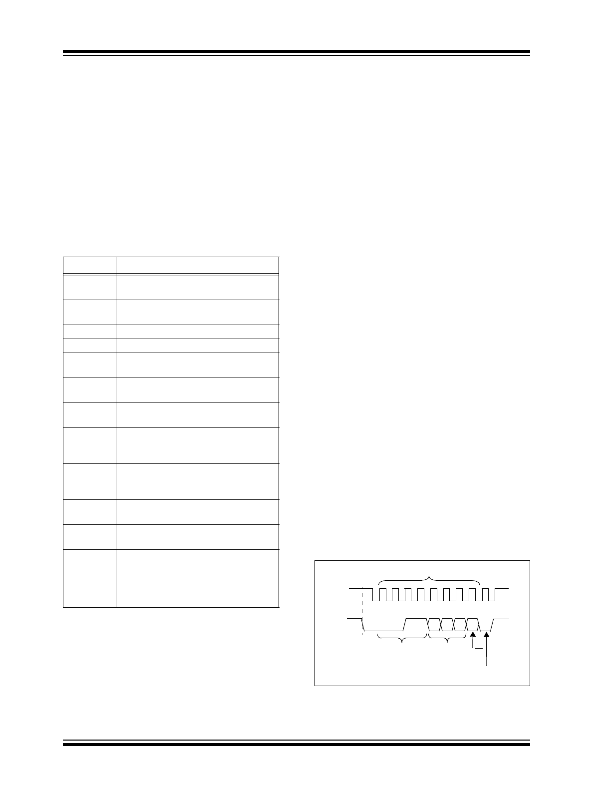
FIGURE 4-1:
Device Addressing.
Term
Description
Master
The device that controls the serial bus,
typically a microcontroller.
Slave
The device addressed by the master,
such as the MCP9844.
Transmitter Device sending data to the bus.
Receiver
Device receiving data from the bus.
START
A unique signal from the master to
initiate serial interface with a slave.
STOP
A unique signal from the master to
terminate serial interface from a slave.
Read/Write A read or write to the MCP9844
registers.
ACK
A receiver Acknowledges (ACK) the
reception of each byte by polling the
bus.
NAK
A receiver Not-Acknowledges (NAK) or
releases the bus to show End-of-Data
(EOD).
Busy
Communication is not possible
because the bus is in use.
Not Busy
The bus is in the Idle state, both SDA
and SCL remain high.
Data Valid
SDA must remain stable before SCL
becomes high in order for a data bit to
be considered valid. During normal
data transfers, SDA only changes state
while SCL is low.
1 2 3 4 5 6 7 8 9
SCL
SDA
0
0
1 1
A2 A1 A0
Start
Address Byte
Slave
Address
R/W
MCP9844
Response
Code
Address
A
C
K

2013 Microchip Technology Inc.
DS20005192B-page 9
MCP9844
4.1.5
DATA VALID
After the Start condition, each bit of data in the
transmission needs to be settled for a time specified by
t
SU-DATA
before SCL toggles from low-to-high (see
Serial Interface Timing Specifications
table).
4.1.6
ACKNOWLEDGE (ACK/NAK)
Each receiving device, when addressed, is obliged to
generate an ACK bit after the reception of each byte.
The master device must generate an extra clock pulse
for ACK to be recognized.
The acknowledging device pulls down the SDA line for
t
SU-DATA
before the low-to-high transition of SCL from
the master. SDA also needs to remain pulled down for
t
H-DATA
after a high-to-low transition of SCL.
During read, the master must signal an End-of-Data
(EOD) to the slave by not generating an ACK bit (NAK)
once the last bit has been clocked out of the slave. In
this case, the slave will leave the data line released to
enable the master to generate the Stop condition.
4.1.7
TIME OUT (T
OUT
)
If the SCL stays low or high for time specified by t
OUT
,
the MCP9844 resets the serial interface. This dictates
the minimum clock speed as specified in the
specification.
MCP9844
DS20005192B-page 10
2013 Microchip Technology Inc.
5.0
FUNCTIONAL DESCRIPTION
The MCP9844 temperature sensors consist of a band
gap type temperature sensor, a Delta-Sigma Analog-to-
Digital Converter (
ADC), user-programmable
registers and a 2-wire I
2
C protocol compatible serial
interface.
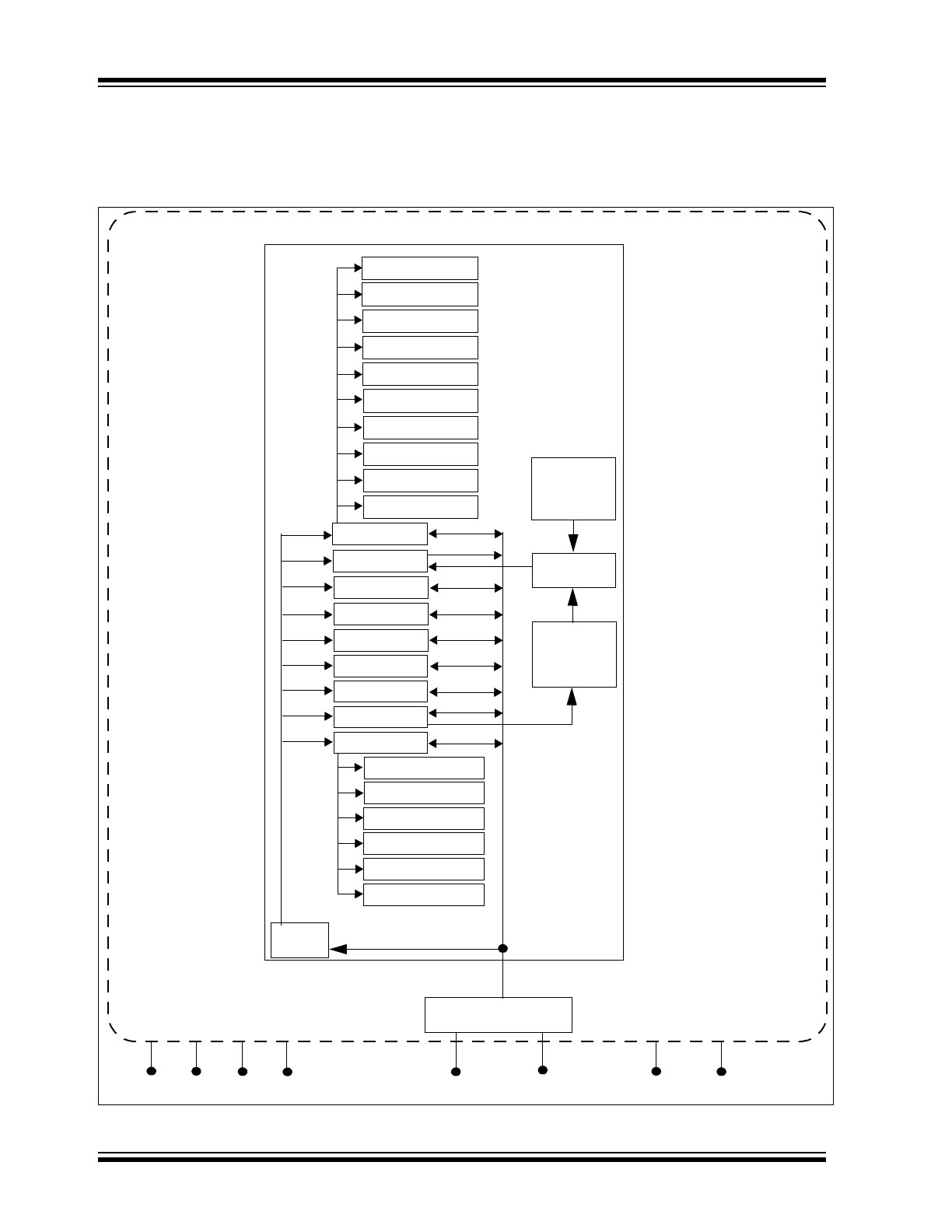
Figure 5-1
shows a block diagram of the
register structure.
FIGURE 5-1:
Functional Block Diagram.
Clear Event
0.5°C/bit
0.25°C/bit
0.125°C/bit
0.0625°C/bit
Temperature
T
UPPER
T
LOWER
Configuration
ADC
Band Gap
Temperature
Sensor
Event Status
Output Control
Critical Event only
Event Polarity
Event Comp./Int.
T
CRIT
Capability
Temp. Range
Accuracy
Output Feature
Register
Pointer
Critical Trip Lock
Alarm Win. Lock Bit
Shutdown
Hysteresis
Manufacturer ID
Resolution
Device ID/Rev.
Selected Resolution
Standard I
2
C
Interface
A0
A1
A2
Event
SDA
SCL
V
DD
GND
I
2
C™ Bus Time-out
Shutdown Status
MCP9844 Temperature Sensor