
2010 Microchip Technology Inc.
DS21909D-page 1
MCP9800/1/2/3
Features:
• Temperature-to-Digital Converter
• Accuracy with 12-bit Resolution:
- ±0.5°C (typical) at +25°C
- ±1°C (maximum) from -10°C to +85°C
- ±2°C (maximum) from -10°C to +125°C
- ±3°C (maximum) from -55°C to +125°C
• User-selectable Resolution: 9-12 bit
• Operating Voltage Range: 2.7V to 5.5V
• 2-wire Interface: I
2
C™/SMBus Compatible
• Operating Current: 200 µA (typical)
• Shutdown Current: 1 µA (maximum)
• Power-saving One-shot Temperature
Measurement
• Available Packages: SOT-23-5, MSOP-8, SOIC-8
Typical Applications:
• Personal Computers and Servers
• Hard Disk Drives and Other PC Peripherals
• Entertainment Systems
• Office Equipment
• Data Communication Equipment
• Mobile Phones
• General Purpose Temperature Monitoring
Typical Application
Description:
Microchip Technology Inc.’s MCP9800/1/2/3 family of
digital temperature sensors converts temperatures
between -55°C and +125°C to a digital word. They
provide an accuracy of ±1°C (maximum) from -10°C to
+85°C.
The MCP9800/1/2/3 family comes with
user-programmable registers that provide flexibility for
temperature sensing applications. The register settings
allow user-selectable 9-bit to 12-bit temperature
measurement resolution, configuration of the
power-saving Shutdown and One-shot (single
conversion on command while in Shutdown) modes
and the specification of both temperature alert output
and hysteresis limits. When the temperature changes
beyond the specified limits, the MCP9800/1/2/3 outputs
an alert signal. The user has the option of setting the
alert output signal polarity as an active-low or
active-high comparator output for thermostat operation,
or as temperature event interrupt output for
microprocessor-based systems.
This sensor has an industry standard 2-wire, I
2
C™/
SMBus compatible serial interface, allowing up to eight
devices to be controlled in a single serial bus. These
features make the MCP9800/1/2/3 ideal for
sophisticated multi-zone temperature-monitoring
applications.
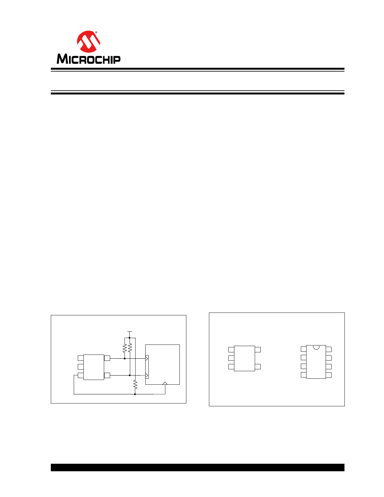
Package Types
PIC
®
V
DD
R
Microcontroller
MCP9800/02
GND
V
DD
ALERT
SDA
SCLK
4
1
2
3
5
I
2
C™ Po
rt
I/O Port
R
PULL-UP
PIC16F737
SDA
GND
ALERT
SCLK
GND
V
DD
ALERT
SDA
SCLK
4
MCP9800
MCP9802
1
2
3
5
SOT-23-5
MCP9801
MCP9803
1
2
3
4
8
7
6
5
SOIC, MSOP
A0
V
DD
A1
A2
MCP9802/03: Serial Bus time-out 35 ms (typ.)
MCP9800/01: No Serial Bus time-out
2-Wire High-Accuracy Temperature Sensor

MCP9800/1/2/3
DS21909D-page 2
2010 Microchip Technology Inc.
NOTES:
2010 Microchip Technology Inc.
DS21909D-page 3
MCP9800/1/2/3
1.0
ELECTRICAL
CHARACTERISTICS
Absolute Maximum Ratings †
V
DD
....................................................................... 6.0V
Voltage at all Input/Output pins .....GND – 0.3V to 5.5V
Storage temperature .......................... -65°C to +150°C
Ambient temp. with power applied ..... -55°C to +125°C
Junction Temperature (T
J
) ................................. 150°C
ESD protection on all pins (HBM:MM) .......(4 kV:400V)
Latch-Up Current at each pin........................ ±200 mA
†Notice: Stresses above those listed under “Maximum
ratings” may cause permanent damage to the device. This is
a stress rating only and functional operation of the device at
those or any other conditions above those indicated in the
operational listings of this specification is not implied.
Exposure to maximum rating conditions for extended periods
may affect device reliability.
DC CHARACTERISTICS
Electrical Specifications: Unless otherwise indicated, V
DD
= 2.7V to 5.5V, GND = Ground, and
T
A
= -55°C to +125°C.
Parameters
Sym
Min
Typ
Max
Unit
Conditions
Power Supply
Operating Voltage Range
V
DD
2.7
—
5.5
V
Operating Current
I
DD
—
200
400
µA
Continuous Operation
Shutdown Current
I
SHDN
—
0.1
1
µA
Shutdown mode
Power-on-Reset Threshold (POR)
V
POR
—
1.7
—
V
V
DD
falling edge
Line Regulation
Δ°C/ΔV
—
0.2
—
°C/V
V
DD
= 2.7V to 5.5V
Temperature Sensor Accuracy
Accuracy with 12-bit Resolution:
T
A
= +25°C
T
ACY
—
±0.5
—
°C
V
DD
= 3.3V
-10°C < T
A
+85°C
T
ACY
-1.0
—
+1.0
°C
V
DD
= 3.3V
-10°C < T
A
+125°C
T
ACY
-2.0
—
+2.0
°C
V
DD
= 3.3V
-55°C < T
A
+125°C
T
ACY
-3.0
—
+3.0
°C
V
DD
= 3.3V
Internal
ADC
Conversion Time:
9-bit Resolution
t
CONV
—
30
75
ms
33 samples/sec (typical)
10-bit Resolution
t
CONV
—
60
150
ms
17 samples/sec (typical)
11-bit Resolution
t
CONV
—
120
300
ms
8 samples/sec (typical)
12-bit Resolution
t
CONV
—
240
600
ms
4 samples/sec (typical)
Alert Output (Open-drain)
High-level Current
I
OH
—
—
1
µA
V
OH
= 5V
Low-level Voltage
V
OL
—
—
0.4
V
I
OL
= 3 mA
Thermal Response
Response Time
t
RES
—
1.4
—
s
Time to 63% (89°C)
27°C (Air) to 125°C (oil bath)
MCP9800/1/2/3
DS21909D-page 4
2010 Microchip Technology Inc.
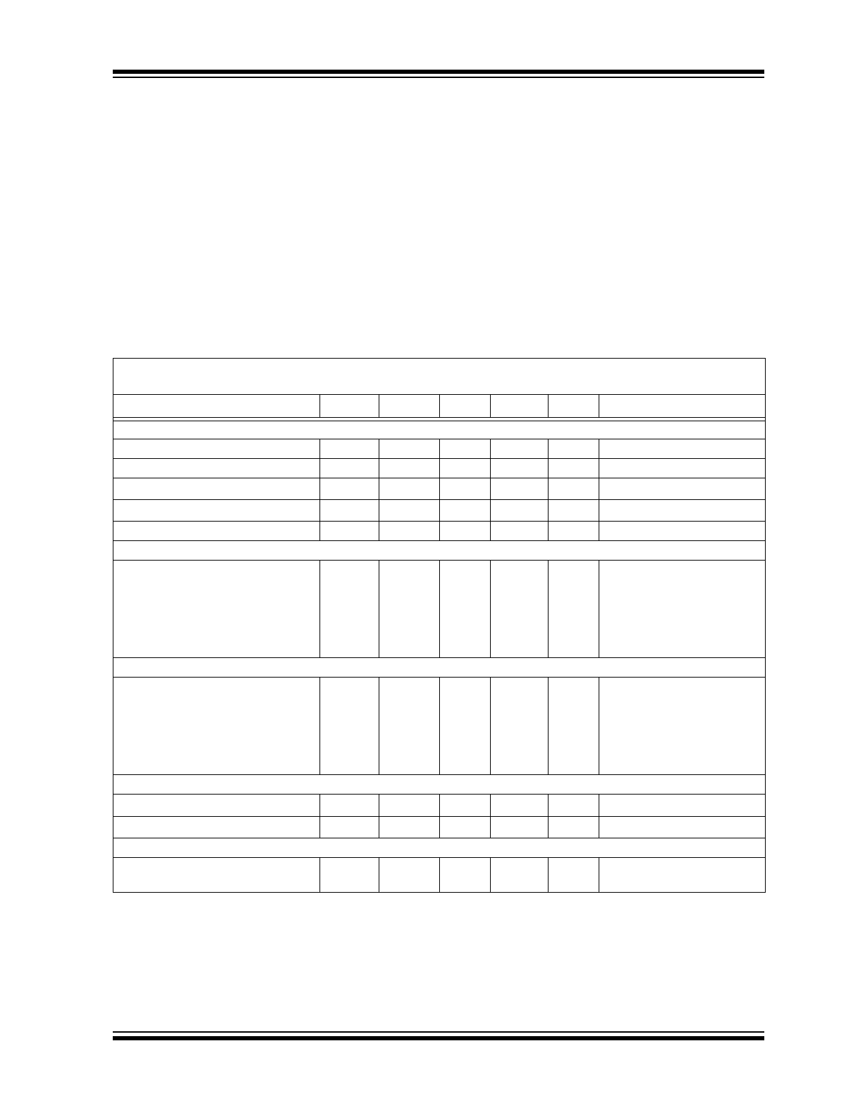
Graphical Symbol Description
DIGITAL INPUT/OUTPUT PIN CHARACTERISTICS
Electrical Specifications: Unless otherwise indicated, V
DD
= 2.7V to 5.5V, GND = Ground and
T
A
= -55°C to +125°C.
Parameters
Sym
Min
Typ
Max
Units
Conditions
Serial Input/Output (SCLK, SDA, A0, A1, A2)
Input
High-level Voltage
V
IH
0.7 V
DD
—
—
V
Low-level Voltage
V
IL
—
—
0.3 V
DD
V
Input Current
I
IN
-1
—
+1
µA
Output (SDA)
Low-level Voltage
V
OL
—
—
0.4
V
I
OL
= 3 mA
High-level Current
I
OH
—
—
1
µA
V
OH
= 5V
Low-level Current
I
OL
6
—
—
mA
V
OL
= 0.6V
Capacitance
C
IN
—
10
—
pF
SDA and SCLK Inputs
Hysteresis
V
HYST
0.05 V
DD
—
—
V
TEMPERATURE CHARACTERISTICS
Electrical Specifications: Unless otherwise indicated, V
DD
= +2.7V to +5.5V, GND = Ground.
Parameters
Sym
Min
Typ
Max
Units
Conditions
Temperature Ranges
Specified Temperature Range
T
A
-55
—
+125
°C
(
Note 1
)
Operating Temperature Range
T
A
-55
—
+125
°C
Storage Temperature Range
T
A
-65
—
+150
°C
Thermal Package Resistances
Thermal Resistance, 5L-SOT23
JA
—
256
—
°C/W
Thermal Resistance, 8L-SOIC
JA
—
163
—
°C/W
Thermal Resistance, 8L-MSOP
JA
—
206
—
°C/W
Note 1:
Operation in this range must not cause T
J
to exceed Maximum Junction Temperature (+150°C).
V
DD
V
IH
V
IL
I
IN
Voltage
Current
Time
Time
V
DD
I
OH
Voltage
Current
Time
Time
INPUT
OUTPUT
V
OL
I
OL
2010 Microchip Technology Inc.
DS21909D-page 5
MCP9800/1/2/3
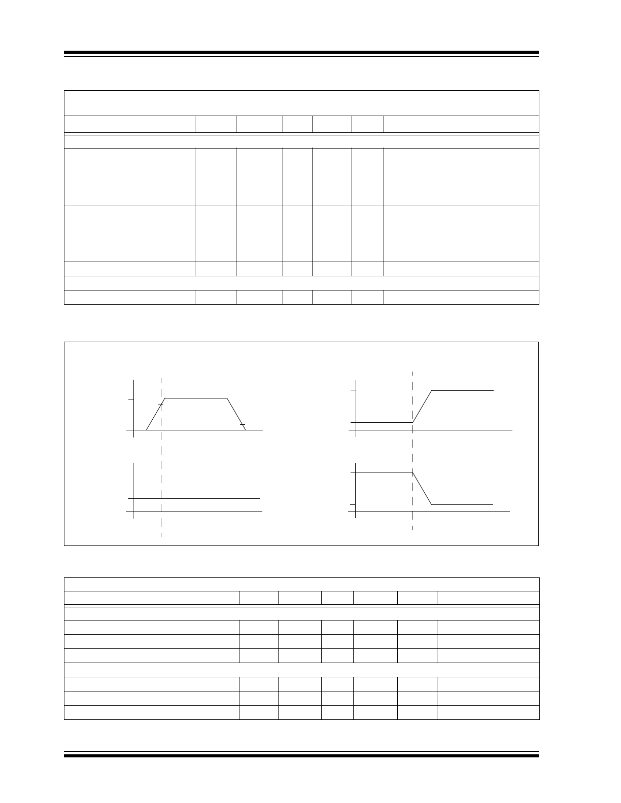
Timing Diagram
SERIAL INTERFACE TIMING SPECIFICATIONS
Electrical Specifications: Unless otherwise indicated, V
DD
= 2.7V to 5.5V, GND = Ground, -55°C < T
A
< +125°C,
C
L
= 80 pF, and all limits measured to 50% point.
Parameters
Sym
Min
Typ
Max
Units
Conditions
2-Wire I
2
C™/SMBus Compatible Interface
Serial Port Frequency
f
SC
0
—
400
kHz
I
2
C MCP9800/01
f
SC
10
—
400
kHz
SMBus MCP9802/03
Clock Period
t
SC
2.5
—
—
µs
Low Clock
t
LOW
1.3
—
—
µs
High Clock
t
HIGH
0.6
—
—
µs
Rise Time
t
R
20
—
300
ns
10% to 90% of V
DD
(SCLK, SDA)
Fall Time
t
F
20
—
300
ns
90% to 10% of V
DD
(SCLK, SDA)
Data Setup Before SCLK High
t
SU-DATA
0.1
—
—
µs
Data Hold After SCLK Low
t
H-DATA
0
—
0.9
µs
Start Condition Setup Time
t
SU-START
0.6
—
—
µs
Start Condition Hold Time
t
H-START
0.6
—
—
µs
Stop Condition Setup Time
t
SU-STOP
0.6
—
—
µs
Bus Idle
t
IDLE
1.3
—
—
µs
Time Out
t
OUT
25
35
50
ms
MCP9802/03 only
t
SU
-S
TA
RT
t
H-S
TA
RT
t
SU
-D
ATA
t
SU
-S
TO
P
t
B-
FR
EE
SCL
SDA
t
H-
DA
TA
t
HI
GH
t
LOW
t
R
, t
F
Start Condition
Data Transmission
Stop Condition

MCP9800/1/2/3
DS21909D-page 6
2010 Microchip Technology Inc.
NOTES:
2010 Microchip Technology Inc.
DS21909D-page 7
MCP9800/1/2/3
2.0
TYPICAL PERFORMANCE CURVES
Note: Unless otherwise noted: V
DD
= 2.7V to 5.5V.
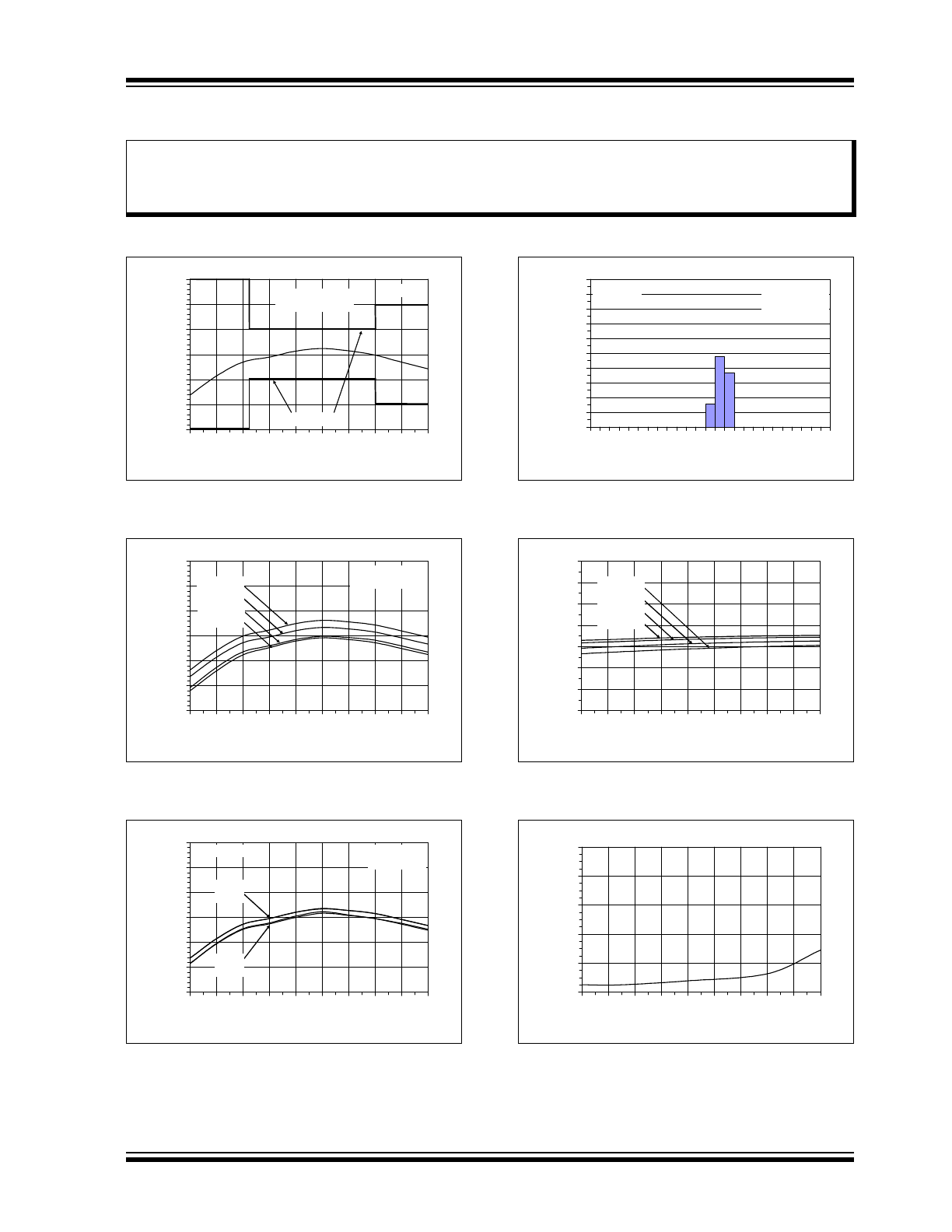
FIGURE 2-1:
Average Temperature
Accuracy vs. Ambient Temperature, V
DD
= 3.3V.
FIGURE 2-2:
Average Temperature
Accuracy vs. Ambient Temperature.
FIGURE 2-3:
Average Temperature
Accuracy vs. Ambient Temperature, V
DD
= 3.3V.
FIGURE 2-4:
Temperature Accuracy
Histogram, T
A
= +25°C.
FIGURE 2-5:
Supply Current vs. Ambient
Temperature.
FIGURE 2-6:
Shutdown Current vs.
Ambient Temperature.
Note:
The graphs and tables provided following this note are a statistical summary based on a limited number of
samples and are provided for informational purposes only. The performance characteristics listed herein
are not tested or guaranteed. In some graphs or tables, the data presented may be outside the specified
operating range (e.g., outside specified power supply range) and therefore, outside the warranted range.
-3.0
-2.0
-1.0
0.0
1.0
2.0
3.0
-55 -35 -15
5
25
45
65
85 105 125
T
A
(°C)
Temp
er
atur
e A
ccu
ra
cy (°C
)
12-Bit Resolution
160 Samples
V
DD
= 3.3V
Spec. Limits
-3.0
-2.0
-1.0
0.0
1.0
2.0
3.0
-55 -35 -15
5
25
45
65
85 105 125
T
A
(°C)
Te
m
p
er
at
ur
e A
ccu
ra
c
y (°
C
)
12-Bit Resolution
160 Samples
V
DD
= 2.7V
V
DD
= 3.3V
V
DD
= 5.5V
V
DD
= 5.0V
-3.0
-2.0
-1.0
0.0
1.0
2.0
3.0
-55 -35 -15
5
25
45
65
85 105 125
T
A
(°C)
T
em
p
er
atu
re
A
ccur
acy
(°C
)
11-Bit
12-Bit
9-Bit
10-Bit
V
DD
= 3.3V
160 Samples
Resolution
0%
10%
20%
30%
40%
50%
60%
70%
80%
90%
100%
-3
.0
-2
.5
-2
.0
-1
.5
-1
.0
-0
.5
0.0
0.5
1.0
1.5
2.0
2.5
3.0
Temperature Accuracy (°C)
Occu
rr
enc
es
T
A
= +25°C
V
DD
= 3.3V
5 lots
32 Samples/lot
160 Samples
50
100
150
200
250
300
350
400
-55 -35 -15
5
25
45
65
85 105 125
T
A
(°C)
I
DD
(µA
)
V
DD
= 2.7V
V
DD
= 3.3V
V
DD
= 5.5V
V
DD
= 5.0V
0
0.2
0.4
0.6
0.8
1
-55 -35 -15
5
25
45
65
85 105 125
T
A
(°C )
I
SH
DN
(µ
A
)
MCP9800/1/2/3
DS21909D-page 8
2010 Microchip Technology Inc.
Note: Unless otherwise noted: V
DD
= 2.7V to 5.5V.
FIGURE 2-7:
ALERT and SDA I
OL
vs.
Ambient Temperature.
FIGURE 2-8:
ALERT and SDA Output
V
OL
vs. Ambient Temperature.
FIGURE 2-9:
MCP980X Thermal
Response vs Time.
6
12
18
24
30
36
42
48
-55 -35 -15
5
25
45
65
85 105 125
T
A
(°C)
AL
E
R
T
&
S
DA
I
OL
(m
A
)
V
DD
= 5.5V
V
DD
= 3.3V
V
DD
= 2.7V
V
OL
= 0.6V
0
0.1
0.2
0.3
0.4
-55 -35 -15
5
25
45
65
85 105 125
T
A
(°C)
AL
ERT
& SDA
V
OL
(V
)
V
DD
= 5.5V
V
DD
= 3.3V
V
DD
= 2.7V
I
OL
= 3mA
5
25
45
65
85
105
125
145
-2
0
2
4
6
8
10
12
14
16
18
20
Time (s)
T
e
m
p
er
atu
re
D
a
ta
(°C
)
SOIC
Average of 10 samples per package
27°C (Air) to 125°C (Oil bath)
MSOP
SOT-23
2010 Microchip Technology Inc.
DS21909D-page 9
MCP9800/1/2/3
3.0
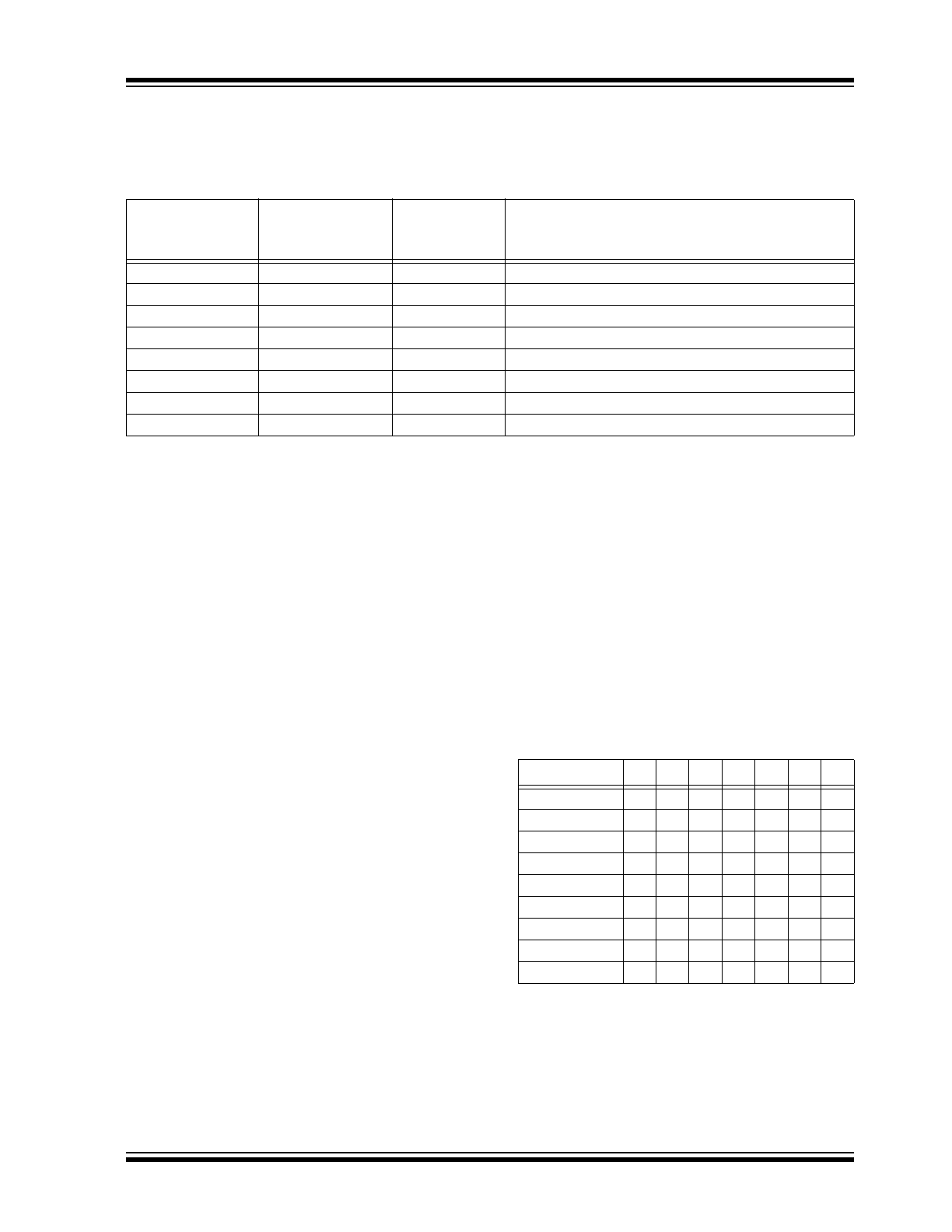
PIN DESCRIPTION
The descriptions of the pins are listed in
Table 3-1
.
TABLE 3-1:
PIN FUNCTION TABLE
3.1
Serial Data Pin (SDA)
The SDA is a bidirectional input/output pin, used to
serially transmit data to and from the host controller.
This pin requires a pull-up resistor to output data.
3.2
Serial Clock Pin (SCLK)
The SCLK is a clock input pin. All communication and
timing is relative to the signal on this pin. The clock is
generated by the host controller on the bus.
3.3
Power Supply Input (V
DD
)
The V
DD
pin is the power pin. The operating voltage, as
specified in the DC electrical specification table, is
applied on this pin.
3.4
Ground (GND)
The GND pin is the system ground pin.
3.5
ALERT Output
The MCP9800/1/2/3’s ALERT pin is an open-drain
output pin. The device outputs an alert signal when the
ambient temperature goes beyond the
user-programmed temperature limit.
3.6
Address Pins (A2, A1, A0)
These pins are device or slave address input pins and
are available only with the MCP9801/03. The device
addresses for the MCP9800/02 are factory-set.
The address pins are the Least Significant bits (LSb) of
the device address bits. The Most Significant bits
(MSb) (A6, A5, A4, A3) are factory-set to <1001>. This
is illustrated in
Table 3-2
.
MCP9800
MCP9802
SOT-23-5
MCP9801
MCP9803
MSOP, SOIC
Symbol
Function
5
1
SDA
Bidirectional Serial Data
4
2
SCLK
Serial Clock Input
3
3
ALERT
Temperature Alert Output
2
4
GND
Ground
—
5
A2
Address Select Pin (bit 2)
—
6
A1
Address Select Pin (bit 1)
—
7
A0
Address Select Pin (bit 0)
1
8
V
DD
Power Supply Input
TABLE 3-2:
SLAVE ADDRESS
Device
A6 A5 A4 A3 A2 A1 A0
MCP9800/02A0 1
0
0
1
0
0
0
MCP9800/02A1 1
0
0
1
0
0
1
MCP9800/02A2
1
0
0
1
0
1
0
MCP9800/02A3
1
0
0
1
0
1
1
MCP9800/02A4
1
0
0
1
1
0
0
MCP9800/02A5
1
0
0
1
1
0
1
MCP9800/02A6
1
0
0
1
1
1
0
MCP9800/02A7
1
0
0
1
1
1
1
MCP9801/03
1
0
0
1
X
X
X
Note:
User-selectable address is shown by X.

MCP9800/1/2/3
DS21909D-page 10
2010 Microchip Technology Inc.
NOTES: