
© 2011 Microchip Technology Inc.
DS22268A-page 1
MCP9501/2/3/4
Features
• Factory Set Temperature Switch
• Available Temperature Switch Thresholds:
- T
SET
= -35°C,-25°C, -15°C, -5°C, 5°C, 15°C,
25°C, 35°C, 45°C, 55°C, 65°C, 75°C, 85°C,
95°C, 105°C, 115°C, 125°C
• Wide Operating Voltage Range: 2.7V to 5.5V
• Low Supply Current: 25 µA (typical)
• Temperature Switch Accuracy:
- ±1°C (typical)
- ±4°C (maximum) -15°C to +75°C
- ±6°C (maximum) -40°C to +125°C
• Switch Threshold Options (Hot/Cold):
- Rising Temp.: MCP9501/2 (Hot Option)
- Falling Temp.: MCP9503/4 (Cold Option)
• Output Configuration Options:
- Active Low, Open-Drain Output: MCP9501/3
– Uses External Pull-up Resistor
- Active-High, Push-Pull Output: MCP9502/4
• User Selectable Hysteresis: 2°C or 10°C (typical)
• 5-lead SOT-23 package
Applications
• Power Supply Critical Temperature Shutdown
• Temperature Alarm
• Thermostat Control
• Fan Control
• Base-Stations
• Automotive
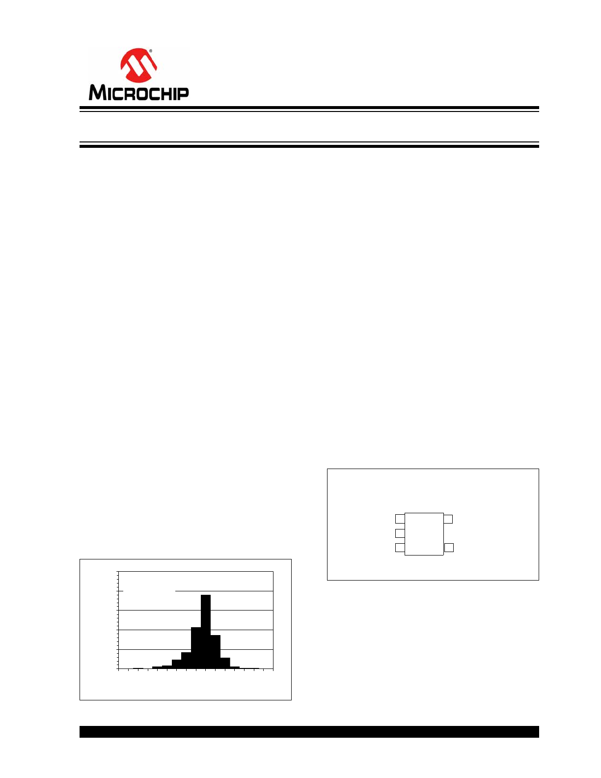
Typical Performance
Description
Microchip Technology’s MCP9501/2/3/4 family of
devices are temperature switches with ±1°C (typical)
accurate factory set output thresholds. These devices
are ideal for high power supply systems where an
overtemperature protection circuit is needed. These
devices do not require external components, consume
25 µA (typical), and the factory set thresholds provide
simplicity.
In addition, this family of devices provide user
selectable 2°C and 10°C (typical) switch hysteresis,
and various output configurations. The MCP9501/2
outputs switch for rising temperatures while the
MCP9503/4 switch for falling temperature, with the
relative hysteresis at the set thresholds. This family of
devices is also available with Active-High Push-Pull
and Active-Low Open-Drain outputs, the MCP9502/4
and the MCP9501/3, respectively. The Push-Pull
output is ideal for a microcontroller interface while the
Open-Drain output can be used for level shifting, wired-
OR configuration, or as a heater on/off switch.
The MCP9501/2/3/4 operate from 2.7V to 5.5V supply.
This family is available with space saving 5-lead
SOT-23 package.
Package Types
0%
10%
20%
30%
40%
50%
-4
.0
-2
.0
0.
0
2.
0
4.
0
Temperature Accuracy (°C)
O
c
c
u
rr
en
ce
s
T
A
= -35°C to 125°C
V
DD
= 4.1V
32 Units
4
1
2
3
5
GND
Hyst
SOT-23-5
MCP9501/2/3/4
GND
Output
V
DD
Temperature Switch with Selectable Hysteresis
MCP9501/2/3/4
DS22268A-page 2
© 2011 Microchip Technology Inc.
OUTPUT FUNCTIONAL DESCRIPTION
Temperature
COLD
HOT
V
Output
Hysteresis
T
HYST
T
SET
MCP9501, Hot-Option (Open-Drain, Active-Low)
Temperature
V
Output
COLD
HOT
Hysteresis
T
HYST
T
SET
MCP9502, Hot-Option (Push-Pull, Active-High)
Temperature
V
Output
COLD
HOT
T
SET
T
HYST
Hysteresis
MCP9503, Cold-Option (Open-Drain, Active-Low)
COLD
HOT
V
Output
Hysteresis
T
SET
T
HYST
MCP9504, Cold-Option (Push-Pull, Active-High)
Temperature
Note:
Available temperature thresholds for
Option P or for rising temperature
only: +5°C, +15°C, +25°C, +35°C,
+45°C, +55°C, +65°C, +75°C, +85°C,
+95°C, +105°C, +115°C, +125°.
Note:
Available temperature thresholds for
Option P or for rising temperature
only: +5°C, +15°C, +25°C, +35°C,
+45°C, +55°C, +65°C, +75°C, +85°C,
+95°C, +105°C, +115°C, +125°.
Note:
Available temperature thresholds for
Option P or for rising temperature
only: +5°C, +15°C, +25°C.
Note:
Available temperature thresholds for
Option N or for falling temperature
only: -35°C, -25°C, -15°C, -5°C.
Note:
Available temperature thresholds for
Option P or for rising temperature only:
+5°C, +15°C, +25°C.
Note:
Available temperature thresholds for
Option N or for falling temperature only:
-35°C, -25°C, -15°C, -5°C.
Note:
Contact Microchip for all other
threshold options.
© 2011 Microchip Technology Inc.
DS22268A-page 3
MCP9501/2/3/4
1.0
ELECTRICAL
CHARACTERISTICS
Absolute Maximum Ratings †
V
DD
.................................................................................. 6.0V
Voltage at all Input/Output pins ............... GND – 0.3V to 6.0V
Input/Output Current .....................................................20 mA
Storage temperature .....................................-65°C to +150°C
Ambient temp. with power applied ................-40°C to +125°C
Junction Temperature (T
J
) .......................................... +150°C
ESD protection on all pins (HBM:MM) ................. (4 kV/400V)
Latch-Up Current at each pin (25°C) ....................... ±200 mA
†Notice: Stresses above those listed under “Maximum
ratings” may cause permanent damage to the device. This is
a stress rating only and functional operation of the device at
those or any other conditions above those indicated in the
operational listings of this specification is not implied.
Exposure to maximum rating conditions for extended periods
may affect device reliability.
DC CHARACTERISTICS
Electrical Specifications: Unless otherwise indicated,
V
DD
= 2.7V to 5.5V, T
A
= -40°C to +125°C, and
GND = Ground.
Parameters
Sym
Min
Typ
Max
Unit
Conditions
Sensor Accuracy
-15°C
≤ T
A
≤ +75°C
-4
±1
+4
°C
Note 1
-40°C
≤ T
A
≤ +125°C
-6
±2
6
°C
Power Supply
Operating Voltage
V
DD
2.7
—
5.5
V
Operating Current
I
DD
—
25
40
µA
Line-Regulation
Δ°C/ΔV
—
0.2
—
°C/V V
DD
= 2.7V to 5.5V
Hysteresis
Trip Point Hysteresis
T
HYST
—
2
—
°C
HYST = GND
—
10
—
°C
HYST = V
DD
Hysteresis Select Input
V
IH
0.8V
DD
—
—
V
V
IL
—
—
0.2V
DD
V
I
Leak
—
0.1
—
µA
Open-Drain Output Leakage
I
Leak
—
0.1
10
µA
MCP9501/3
Output Voltage High
V
OH
0.8V
DD
—
—
V
I
OUT
= 5 mA (MCP9502/4)
Output Voltage Low
V
OL
—
—
0.2V
DD
V
I
OUT
= 5 mA
Turn On Time
T
ON
—
1
—
ms
SOT23-5
t
RES
—
1.7
—
s
Time to 63% (89°C).
+25°C (Air) to +125°C
(oil bath)
Note 1:
This specification is tested at mid supply of 4.1V for optimum operation across the supply voltage range of
2.7V to 5.5V.
TEMPERATURE CHARACTERISTICS
Electrical Specifications: Unless otherwise indicated,
V
DD
= 2.7V to 5.5V, T
A
= -40°C to +125°C, and
GND = Ground.
Parameters
Sym
Min
Typ
Max
Units
Conditions
Temperature Ranges
Specified Temperature Range
T
A
-40
—
+125
°C
(
Note 1
)
Operating Temperature Range
T
A
-40
—
+125
°C
Storage Temperature Range
T
A
-65
—
+150
°C
Thermal Package Resistances
Thermal Resistance, 5L-SOT23
θ
JA
—
220.7
—
°C/
Ω
Note 1:
Operation in this range must not cause T
J
to exceed Maximum Junction Temperature (+150°C).
MCP9501/2/3/4
DS22268A-page 4
© 2011 Microchip Technology Inc.
2.0
TYPICAL PERFORMANCE CURVES
Note: Unless otherwise indicated, V
DD
= 2.7V to 5.5V, T
A
= -40°C to +125°C, GND = Ground, R
PULL-UP
= 10 k
Ω
(MCP9501/3 only) and 0.1 µF bypass capacitor.
FIGURE 2-1:
Temperature Accuracy.
FIGURE 2-2:
Hysteresis vs. Temperature.
FIGURE 2-3:
Supply Current vs.
Temperature.
FIGURE 2-4:
Leakage vs. Temperature.
FIGURE 2-5:
V
OL
,
V
OH
vs. Temperature.
FIGURE 2-6:
Power On Reset Threshold
vs. Temperature.
Note:
The graphs and tables provided following this note are a statistical summary based on a limited number of
samples and are provided for informational purposes only. The performance characteristics listed herein
are not tested or guaranteed. In some graphs or tables, the data presented may be outside the specified
operating range (e.g., outside specified power supply range) and therefore outside the warranted range.
-6.0
-4.0
-2.0
0.0
2.0
4.0
6.0
-40
-20
0
20
40
60
80
100
120
T
A
(°C)
Te
m
p
e
rature
A
c
c
u
rac
y
(°
C
)
Spec. Limits
+ St. Dev.
Average
- St. Dev.
V
DD
= 4.1V
32 units
0.0
0.5
1.0
1.5
2.0
2.5
3.0
3.5
4.0
-40 -20
0
20
40
60
80 100 120
T
A
(°C)
HY
ST
=
V
SS
, Hy
st
ere
s
is
(°
C)
6.0
7.0
8.0
9.0
10.0
11.0
12.0
13.0
14.0
HY
S
T
=
V
DD
, H
yst
e
resis
(°
C
)
HYST = V
SS
HYST = V
DD
10
15
20
25
30
35
40
-40
-20
0
20
40
60
80
100
120
T
A
(°C)
I
DD
(µA
)
V
DD
= 5.5V
V
DD
= 4.1V
V
DD
= 2.7V
0.00
0.02
0.04
0.06
0.08
0.10
-40
-20
0
20
40
60
80
100
120
T
A
(°C)
Le
ak
ag
e
(µA
)
HYST Input Pin
Open-Drain Output
(MCP9501/03 only)
0%
5%
10%
15%
20%
-40 -20
0
20
40
60
80 100 120
T
A
(°C)
V
OL
(%
o
f V
DD
)
80%
85%
90%
95%
100%
V
OH
(%
o
f V
DD
)
V
OH
, V
DD
= 5.5V
V
OH
, V
DD
= 4.1V
V
OH
, V
DD
= 2.7V
V
OL
, V
DD
= 5.5V
V
OL
, V
DD
= 4.1V
V
OL
, V
DD
= 2.7V
V
POR
Hyst
er
e
s
is (
m
V
)
45
55
65
75
85
95
105
0.0
0.5
1.0
1.5
2.0
2.5
3.0
-40
-20
0
20
40
60
80
100 120
V
P
O
R
H
y
s
te
re
s
is
(
m
V
)
V
P
O
R
(V
)
T
A
(°C)
V
POR
Hysteresis
V
POR
(V
)
V
POR
H
y
ste
resis
(m
V
)
© 2011 Microchip Technology Inc.
DS22268A-page 5
MCP9501/2/3/4
Note: Unless otherwise indicated, V
DD
= 2.7V to 5.5V, T
A
= -40°C to +125°C, GND = Ground, R
PULL-UP
= 10 k
Ω
(MCP9501 only) and 0.1 µF bypass capacitor.
FIGURE 2-7:
Temperature Accuracy
Distribution at -15°C.
FIGURE 2-8:
Temperature Accuracy
Distribution at 5°C.
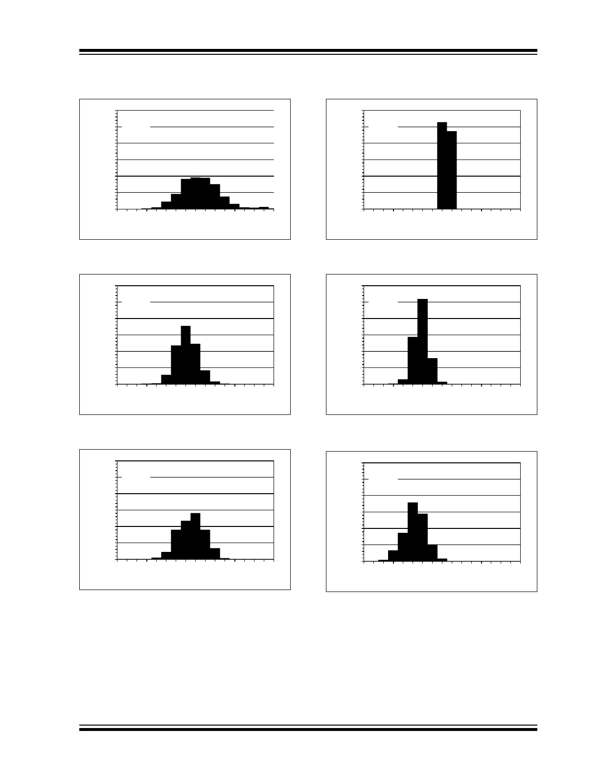
FIGURE 2-9:
Temperature Accuracy
Distribution at 65°C.
FIGURE 2-10:
Temperature Accuracy
Distribution at 105°C.
FIGURE 2-11:
Temperature Accuracy
Distribution at 115°C.
FIGURE 2-12:
Temperature Accuracy
Distribution at 125°C.
0%
10%
20%
30%
40%
50%
60%
-4
.0
-2
.0
0
.0
2
.0
4
.0
O
c
c
u
rr
e
n
c
e
s
Temperature Accuracy (°C)
T
A
= -15\ C
V
DD
= 4.1V
492 Units
°
O
c
c
u
rre
nc
e
s
T
A
(°C)
-4.
0
-2.
0
0.
0
2.
0
4.
0
0%
10%
20%
30%
40%
50%
60%
-4
.0
-2
.0
0
.0
2
.0
4
.0
O
c
c
u
rr
e
n
c
e
s
Temperature Accuracy (°C)
T
A
= 5\ C
V
DD
= 4.1V
480 Units
Oc
cu
rr
en
ce
s
°
-4
.0
-2
.0
0.
0
2.
0
4.
0
T
A
(°C)
0%
10%
20%
30%
40%
50%
60%
-4
.0
-2
.0
0
.0
2
.0
4
.0
O
c
c
u
rr
e
n
c
e
s
Temperature Accuracy (°C)
T
A
= 65\ C
V
DD
= 4.1V
480 Units
°
T
A
(°C)
-4
.0
-2
.0
0.
0
2.
0
4.
0
Oc
cu
rr
en
ce
s
-4
.0
-2
.0
0.0
2.0
4.0
T
A
(°C)
-4
.0
-2
.0
0.0
2.0
4.0
T
A
(°C)
°
O
c
c
u
rre
nc
e
s
0%
10%
20%
30%
40%
50%
60%
-4
.0
-2
.0
0
.0
2
.0
4
.0
O
c
c
u
rr
e
n
c
e
s
Temperature Accuracy (°C)
T
A
= 105\ C
V
DD
= 4.1V
480 Units
°
Oc
cu
rr
en
ce
s
T
A
(°C)
-4
.0
-2
.0
0.0
2.0
4.0
0%
10%
20%
30%
40%
50%
60%
-4
.0
-2
.0
0
.0
2
.0
4
.0
O
c
c
u
rr
e
n
c
e
s
Temperature Accuracy (°C)
T
A
= 115\ C
V
DD
= 4.1V
480 Units
-4
.0
-2
.0
0.
0
2.
0
4.
0
°
T
A
(°C)
Oc
c
u
rr
en
ce
s
°
0%
10%
20%
30%
40%
50%
60%
-4
.0
-2
.0
0
.0
2
.0
4
.0
O
c
c
u
rr
e
n
c
e
s
Temperature Accuracy (°C)
T
A
= 125\ C
V
DD
= 4.1V
480 Units
Oc
cu
rr
e
n
ce
s
T
A
(°C)
-4
.0
-2
.0
0.0
2.0
4.0
°

MCP9501/2/3/4
DS22268A-page 6
© 2011 Microchip Technology Inc.
3.0
PIN DESCRIPTIONS
TABLE 3-1:
PIN FUNCTION TABLE
3.1
Ground (GND)
The GND pin is the system ground pin. Pin 2 must be
connected to system ground. Pin 1 can also be
connected to system ground which would provide
better thermal conduction to the die.
3.2
Hysteresis Input (HYS)
This is an input pin which can be connected to V
DD
or
GND to select output hysteresis. Either 2°C
(HYST = GND) or 10°C (HYST = V
DD
)
of typical
hysteresis can be selected.
3.3
Power Pin (V
DD
)
The operating voltage range, as specified in the DC
electrical specification table, is applied on this pin.
3.4
Switch Output (Output)
This output is triggered when temperature rises or falls
beyond the programmed trip temperature threshold.
MCP9501/3 require an external pull-up resistor.
MCP9501/2/3/4
Symbol
Description
SOT-23-5
1
GND
Ground
2
GND
Ground (must be connected to ground)
3
HYST
Hysteresis Selection Input:
HYST = GND
→ Hysteresis is 2°C (typical)
HYST = V
DD
→ Hysteresis is 10°C (typical)
4
V
DD
Power pin
5
Output
Output Options:
MCP9501
→ Open-Drain, Active-Low Output (Hot-Option)
MCP9502
→ Push-Pull, Active-High Output (Hot-Option)
MCP9503
→ Open-Drain, Active-Low Output (Cold-Option)
MCP9504
→ Push-Pull, Active-High Output (Cold-Option)

© 2011 Microchip Technology Inc.
DS22268A-page 7
MCP9501/2/3/4
NOTES:
MCP9501/2/3/4
DS22268A-page 8
© 2011 Microchip Technology Inc.
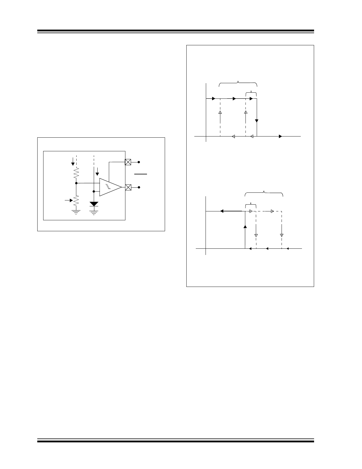
4.0
FUNCTIONAL DESCRIPTION
The MCP9501/2/3/4 temperature switch family
integrates a thermal diode, a comparator, and a factory
selectable resistive network used to set the
temperature thresholds. The available output
thresholds range from -35°C to 125°C at 10°C
increments. There is no additional configuration
required to operate this device. The selectable output
hysteresis is controlled using a single input pin. When
this pin is connected to ground, the output hysteresis is
2°C (typical) and when connected to V
DD
the output
hysteresis is 10°C (typical).
Figure 4-1
shows the
functional block diagram.
FIGURE 4-1:
Functional Block Diagram.
There are two output configurations for this family, a
push-pull and an open-drain output with active-high
and active-low assertions. These assertion options are
referred to as Cold and Hot options, primarily due to the
direction of selected hysteresis. For the Cold option,
temperature has to fall below the threshold for the
output to assert High, and de-assert Low when the
temperature rises above the threshold plus the
hysteresis. For example, a 65°C threshold and 2°C
(typical) hysteresis, when temperature falls below 65°C
the output asserts High, and the de-asserts Low when
temperature rises above 67°C. For the Hot option, the
opposite is true. When temperature rises above 65°C,
the output asserts Low, and de-asserts High when the
temperature falls below 63°C.
Figure 4-2
shows a
graphical description for the Hot and Cold options.
FIGURE 4-2:
Output Hysteresis.
The Push-Pull output is ideal for a microcontroller
interface using an input/output pin or an interrupt input
pin. The open-drain option can be used with multiple
sensors in a wired-OR configuration or as a level
shifter.
I
SET
R
x
+
-
OUT/
OUT
Thermal
Diode
Hysteresis
Select Pin
Threshold
Select
Cold
Hot
T
SET
T
HYST
Temperature
V
O
u
tput
10°C Typical Hysteresis
2°C Typical
Hysteresis
Cold
Hot
T
SET
T
HYST
Temperature
V
O
u
tput
10°C Typical Hysteresis
2°C Typical
Hysteresis
Hot-Option (Active-Low)
Cold-Option (Active-High)
© 2011 Microchip Technology Inc.
DS22268A-page 9
MCP9501/2/3/4
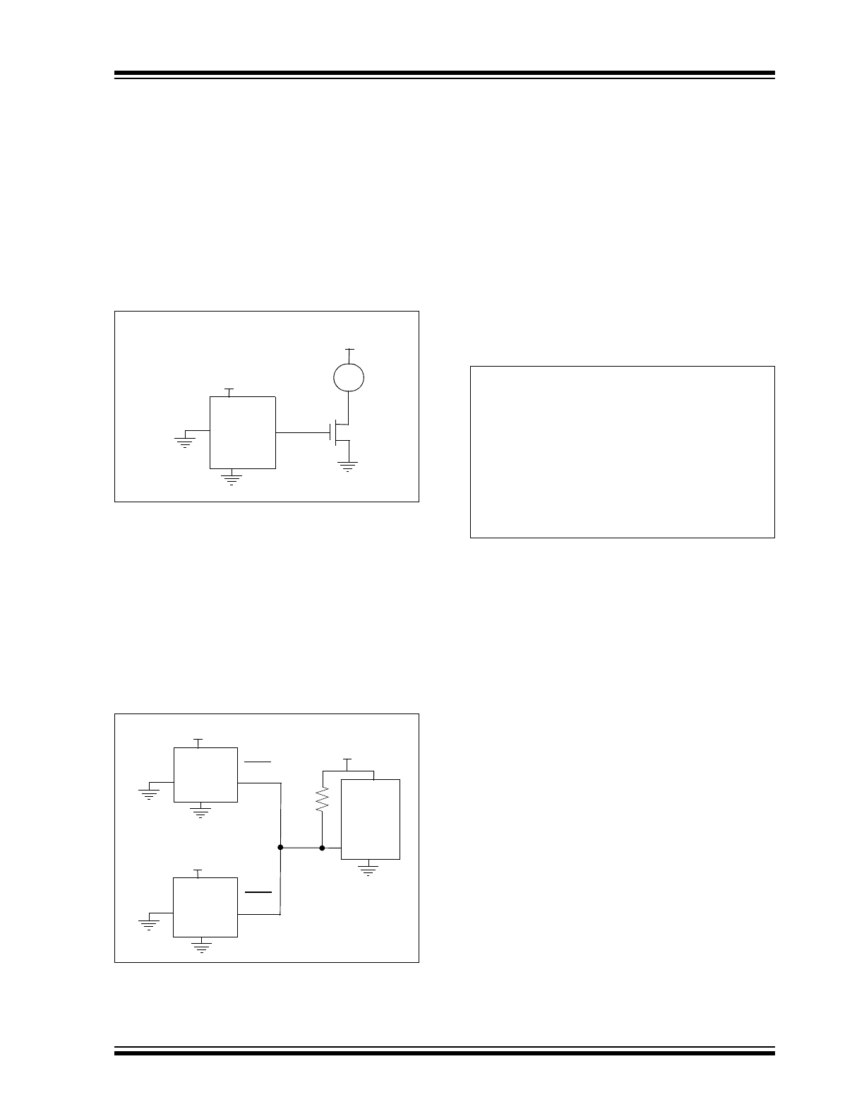
4.1
Application Information
The MCP9501/2/3/4 temperature switch family
integrates a temperature sensor and a comparator
circuit which outputs an alert signal when the factory
set temperature threshold is exceeded. No additional
component is required for device operation, which
provides simplicity to the system designer. The device
output options provide design flexibility for various
applications such as overtemperature protection circuit
or a closed loop temperature control unit. This device
can be interfaced to a closed loop fan controller
network without the need for a microcontroller.
FIGURE 4-3:
Fan Controller Using
MCP9502.
The MCP9501/2/3/4 provide Open-Drain output where
multiple sensors from multiple PCB hot-spots can be
connected to a single processor I/O input with a wired-
OR configuration. The MCP9501 requires an external
pull-up resistor which can be used to level-shift the alert
signal. For example, if the sensors are powered with
5V
DD
and the controller or processor is powered with
3V
DD
, the external resistor can be level-shifted by
connecting 3V
DD
to the pull-up resistor as shown in
Figure 4-4
.
FIGURE 4-4:
MCP9501 Wired-OR Output
Configuration with Level-shift.
4.1.1
LAYOUT CONSIDERATION AND
THERMAL CONSIDERATION
This family of sensors measures temperature by
monitoring the voltage level of a thermal diode located
in the die. A low-impedance thermal path between the
die and the PCB is provided by the pins. Therefore, the
sensor effectively monitors PCB temperature. For
efficient performance, it is recommended to layout the
device as close to the heat source as possible.
When connecting an external resistor to the MCP9501/
3, the current through the pull-up resistor must be
considered to prevent self-heat due to power. This can
be determined using
Equation 4-1
.
EQUATION 4-1:
EFFECT OF
SELF-HEATING
For example, at room temperature, when the output
asserts Active-Low and maximum I
DD
= 50 µA,
V
DD
= 5.5V, V
OL
= 0.3V and I
OUT
= 5 mA (see the
specification table), the self heating due to power
dissipation (T
J
- T
A
) is ~0.4°C.
Output
HYST
5V
DD
MCP9502
12V
M
OUT
HYST
5V
DD
OUT
HYST
5V
DD
I/O
R
P
U
L
L_U
P
Micro-
controller
MCP9501
85°C
MCP9503
35°C
3V
DD
Where:
T
J
=
Junction Temperature
T
A
=
Ambient Temperature
θ
JA
=
Package Thermal Resistance
(220.7 °C/W)
V
OL
=
Sensor Output Low Voltage
I
OUT
=
Output Current
T
J
T
A
–
θ
JA
V
DD
I
DD
×
V
OL
I
OUT
×
+
(
)
=
MCP9501/2/3/4
DS22268A-page 10
© 2011 Microchip Technology Inc.
4.1.2
POWER SUPPLY REJECTION
The MCP9501/2/3/4 family does not require any
additional components. However, it is recommended
that a decoupling capacitor of 0.1 µF to 1 µF be used
between the V
DD
and GND pins. A high-frequency
ceramic capacitor is recommended. It is necessary for
the capacitor to be located as close as possible to the
power pins in order to provide effective noise
protection.
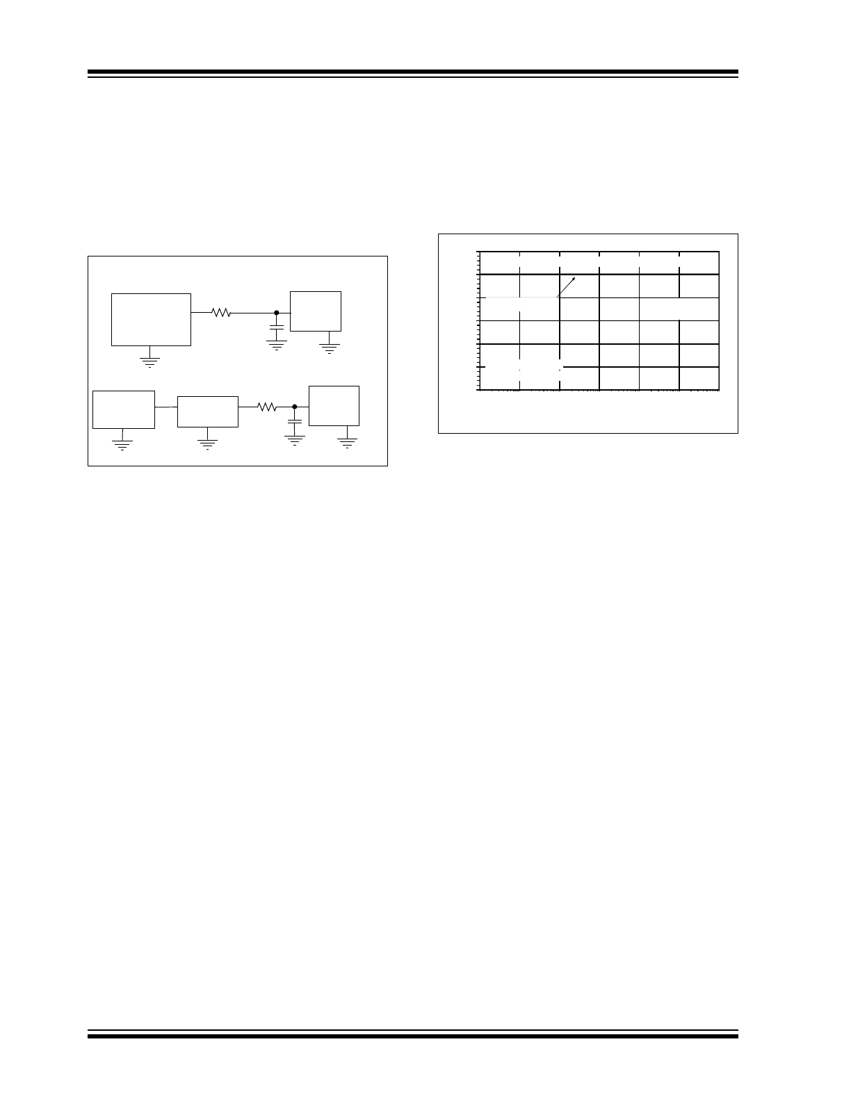
FIGURE 4-5:
Power-supply Filter using a
Single Resistor.
For applications where a switching regulator is used to
power the sensor, it is recommended to add a 200
Ω
resistor in series to V
DD
to filter out the switcher noise.
It is also recommended to add the series resistor in
applications where a linear regulator is used to
step-down a switching regulator voltage to power the
sensor, as shown in
Figure 4-5
. For example, if a
linearly regulated 3.3V from a 5V switching regulator is
used to power the sensor, add a 200
Ω series resistor.
The MCP9501/2/3/4 family of sensors is designed to
prevent false output trigger due to high frequency
power supply or system noise.
Figure 4-6
shows the
device performance with a high frequency signal added
on V
DD
. The output is not triggered due to the signal
added on V
DD
. With some applications, it is
recommended to add a bypass capacitor of 0.1 µF to
1 µF.
FIGURE 4-6:
Power Supply Rejection.
V
DD
200
Ω
MCP9501/2/3/4
Switching
Regulator
0.1 µF
bypass
V
DD
200
Ω
MCP9501/2/3/4
Switching
Regulator
0.1 µF
bypass
Regulator
Linear
0
1
2
3
4
5
6
10
100
1000
10000
100000
1000000
10000000
O
u
tp
u
t
V
o
lt
a
g
e
(
V
)
Frequency (Hz)
MCP9501/2/3/4 T
SET
= 25\ C Power Supply Rejection
No False Trigger
1
0
k
1
0
0
k
1
M
1
0
M
1
k
1
0
0
1
0
V
DD
= 5V + 400mV
AC
V
DD
= 5V + 400mV
SQR
T
SET
= 25\ C
T
A
= 23\ C
°
°
°
Frequency (Hz)
Ou
tp
ut
V
o
lt
ag
e (
V
)