
2012 Microchip Technology Inc.
DS25133B-page 1
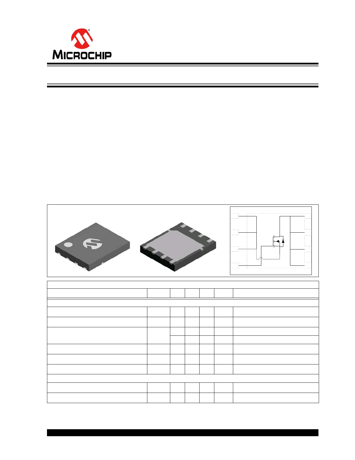
MCP87022
Features:
• Low Drain-to-Source On Resistance (R
DS(ON)
)
• Low Total Gate Charge (Q
G
) and Gate-to-Drain
Charge (Q
GD
)
• Low Series Gate Resistance (R
G
)
• Fast Switching
• Capable of Short Dead-Time Operation
• ROHS Compliant
Applications
• Point-of-Load DC-DC Converters
• High Efficiency Power Management in Servers,
Networking and Automotive Applications
Description
The MCP87022 is an N-Channel power MOSFET in a
popular PDFN 5 mm x 6 mm package. Advanced
packaging and silicon processing technologies allow
the MCP87022 to achieve a low Q
G
for a given R
DS(on)
value, resulting in a low Figure of Merit (FOM).
Combined with low R
G
, the low Figure of Merit of the
MCP87022 allows high efficiency power conversion
with reduced switching and conduction losses.
Package Type
Product Summary Table:
Unless otherwise indicated, T
A
= +25˚C
Parameters
Sym
Min
Typ
Max
Units Conditions
Operating Characteristics
Drain-to-Source Breakdown Voltage
BV
DSS
25
—
—
V
V
GS
= 0V, I
D
= 250 µA
Gate-to-Source Threshold Voltage
V
GS(TH)
1
1.3
1.6
V
V
DS
= V
GS
, I
D
= 250 µA
Drain-to-Source On Resistance
R
DS(ON)
—
2.2
2.6
mΩ
V
GS
= 4.5V, I
D
= 25A
—
1.9
2.3
mΩ
V
GS
= 10V, I
D
= 25A
Total Gate Charge
Q
G
—
25.5
29
nC
V
DS
= 12.5V, I
D
= 25A, V
GS
= 4.5V
Gate-to-Drain Charge
Q
GD
—
9
—
nC
V
DS
= 12.5V, I
D
= 25A
Series Gate Resistance
R
G
—
1.3
—
Ω
—
Thermal Characteristics
Thermal Resistance Junction-to-X
R
θJX
—
—
56
˚C/W
Note 1
Thermal Resistance Junction-to-Case
R
θJC
—
—
1.6
˚C/W
Note 2
Note
1:
R
θJX
is determined with the device surface mounted on a 4-Layer FR4 PCB, with a 1” x 1” mounting pad of
2 oz. copper. This characteristic is dependent on user’s board design.
2:
R
θJC
is determined using JEDEC 51-14 Method. This characteristic is determined by design.
S
G
S
S
D
D
D
D
1
2
3
4
5
6
7
8
PDFN 5 x 6
High-Speed N-Channel Power MOSFET
MCP87022
DS25133B-page 2
2012 Microchip Technology Inc.
1.0
ELECTRICAL
CHARACTERISTICS
Absolute Maximum Ratings †
V
DS
.......................................................................+25V
V
GS
........................................................... +10.0V / -8V
I
D,
Continuous ....................................100A, T
C
= 25˚C
P
D
..................................................... 2.2W, T
A
= +25˚C
T
J
, T
STG
.............................................. -55˚C to +150˚C
E
AS
Avalanche Energy ..................................... 450 mJ
I
D
= 30A, L = 1 mH, R
G
= 25Ω
† Notice:
Stresses above those listed under
“Maximum Ratings” may cause permanent damage to
the device. This is a stress rating only and functional
operation of the device at those or any other conditions
above those indicated in the operational sections of this
specification is not intended. Exposure to maximum
rating conditions for extended periods may affect
device reliability.
DC ELECTRICAL CHARACTERISTICS
Electrical Characteristics:
Unless otherwise indicated, T
A
= +25°C
Parameters
Sym
Min
Typ
Max
Units Conditions
Static Characteristics
Drain-to-Source
Breakdown Voltage
B
VDSS
25
—
—
V
V
GS
= 0V, I
D
= 250 µA
Drain-to-Source Leakage Current
I
DSS
—
—
1
µA
V
GS
= 0V, V
DS
= 20V
Gate-to-Source Leakage Current
I
GSS
—
—
100
nA
V
DS
= 0V, V
GS
= 10V/-8V
Gate-to-Source Threshold Voltage
V
GS(TH)
1
1.3
1.6
V
V
DS
= V
GS
, I
D
= 250 µA
Drain-to-Source On Resistance
R
DS(ON)
—
2.2
2.6
m
V
GS
= 4.5V, I
D
= 25 A
—
1.9
2.3
m
V
GS
= 10V, I
D
= 25 A
Transconductance
g
fs
—
155
—
S
V
DS
= 12.5V, I
D
= 25A
Dynamic Characteristics
Input Capacitance
C
ISS
—
2310
—
pF
V
GS
= 0V, V
DS
= 12.5V, f = 1 MHz
Output Capacitance
C
OSS
—
1080
—
pF
V
GS
= 0V, V
DS
= 12.5V, f = 1 MHz
Reverse Transfer Capacitance
C
RSS
—
285
—
pF
V
GS
= 0V, V
DS
= 12.5V, f = 1 MHz
Total Gate Charge
Q
G
—
25.5
29
nC
V
DS
= 12.5V, I
D
= 25 A,
V
GS
= 4.5V
Gate-to-Drain Charge
Q
GD
—
9
—
nC
V
DS
= 12.5V, I
D
= 25 A
Gate-to-Source Charge
Q
GS
—
4.5
—
nC
V
DS
= 12.5V, I
D
= 25 A
Gate Charge at V
GS(TH)
Q
G(TH)
—
3.3
—
nC
V
DS
= 12.5V, I
D
= 25 A
Output Charge
Q
OSS
—
21
—
nC
V
DS
= 12.5V, V
GS
= 0
Turn-On Delay Time
t
d(on)
—
7.6
—
ns
V
DS
= 12.5V, V
GS
= 4.5V,
I
D
= 25A, R
G
= 2
Rise Time
t
r
—
27
—
ns
V
DS
= 12.5V, V
GS
= 4.5V,
I
D
= 25A, R
G
= 2
Turn-Off Delay Time
t
d(off)
—
21
—
ns
V
DS
= 12.5V, V
GS
= 4.5V,
I
D
= 25A, R
G
= 2
Fall Time
t
f
—
17
—
ns
V
DS
= 12.5V, V
GS
= 4.5V,
I
D
= 25A, R
G
= 2
Series Gate Resistance
R
G
—
1.3
—
2012 Microchip Technology Inc.
DS25133B-page 3
MCP87022
Diode Characteristics
Diode Forward Voltage
V
FD
—
0.8
1
V
I
S
= 25A, V
GS
= 0V
Reverse Recovery Charge
Q
RR
—
39
—
nC
I
S
= 25A, di/dt = 300 A/µs
Reverse Recovery Time
t
rr
—
22
—
ns
I
S
= 25A, di/dt = 300 A/µs
Avalanche Characteristics
Avalanche Energy
E
AS
200
—
—
mJ
I
D
= 20A, L = 1 mH,
R
G
= 25
TEMPERATURE CHARACTERISTICS
Electrical Characteristics: Unless otherwise indicated, T
A
= +25°C
Parameters
Sym
Min
Typ
Max
Units
Conditions
Temperature Ranges
Operating Junction Temperature Range
T
J
-55
—
150
°C
Storage Temperature Range
T
A
-55
—
150
°C
Package Thermal Resistances
Thermal Resistance Junction-to-X, 8L 5x6-PDFN
R
θJX
—
—
56
°C/W
Note 1
Thermal Resistance Junction-to-Case, 8L 5x6-PDFN
R
θJC
—
—
1.6
°C/W
Note 2
Note 1:
R
θJX
is determined with the device surface mounted on a 4-Layer FR4 PCB, with a 1” x 1” mounting pad of
2 oz. copper. This characteristic is dependent on user’s board design.
2:
R
θJC
is determined using JEDEC 51-14 Method. This characteristic is determined by design.
DC ELECTRICAL CHARACTERISTICS (CONTINUED)
Electrical Characteristics:
Unless otherwise indicated, T
A
= +25°C
Parameters
Sym
Min
Typ
Max
Units Conditions
MCP87022
DS25133B-page 4
2012 Microchip Technology Inc.
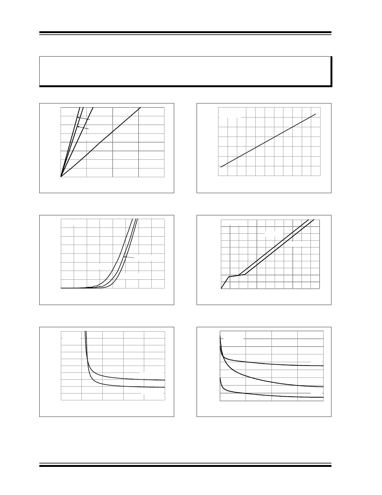
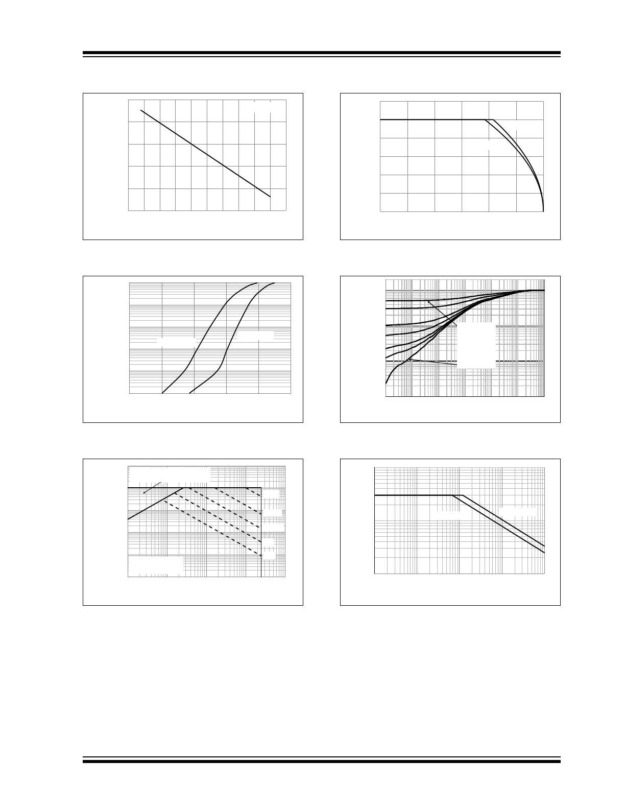
2.0
TYPICAL PERFORMANCE CURVES
Note:
Unless otherwise indicated, T
A
= +25°C.
FIGURE 2-1:
Typical Output
Characteristics.
FIGURE 2-2:
Typical Transfer
Characteristics.
FIGURE 2-3:
On Resistance vs. Gate-to-
Source Voltage.
FIGURE 2-4:
Normalized On Resistance
vs. Temperature.
FIGURE 2-5:
Gate-to-Source Voltage vs.
Gate Charge.
FIGURE 2-6:
Capacitance vs. Drain-to-
Source Voltage.
Note:
The graphs and tables provided following this note are a statistical summary based on a limited number of
samples and are provided for informational purposes only. The performance characteristics listed herein
are not tested or guaranteed. In some graphs or tables, the data presented may be outside the specified
operating range (e.g., outside specified power supply range) and therefore outside the warranted range.
0
10
20
30
40
50
60
70
80
0.0
0.2
0.4
0.6
0.8
V
DS
- Drain-to-Source Voltage (V)
V
GS
= 2.5V
V
GS
= 3V
V
GS
= 10V
V
GS
= 4.5V
I
D
-
D
rai
n
C
u
rr
en
t (
A
)
0
10
20
30
40
50
60
70
80
1 1.25 1.5 1.75 2 2.25 2.5 2.75 3
I
D
-
Drain Current
(A)
V
GS
- Gate-to-Source Voltage (V)
T
C
= +25
°C
T
C
= +125
°C
V
DS
= 5V
T
C
= -55
°C
I
D
-
Dr
a
in
Cu
rr
e
n
t (
A
)
0
1
2
3
4
5
6
7
8
9
10
0
2
4
6
8
10
V
GS
- Gate-to-Source Voltage (V)
T
C
= +25°C
T
C
= +125°C
I
D
= 25A
R
DS
(O
N
)
- O
n
-S
ta
te
R
e
s
ist
an
ce
(m
Ω
)
0.4
0.6
0.8
1
1.2
1.4
1.6
1.8
-60 -40 -20 0 20 40 60 80 100
120
140 160
Normalized On-State Resistance
T
C
- Case Temperature (
°C)
I
D
= 25A
V
GS
= 4.5V
0
1
2
3
4
5
6
7
8
9
10
0
5
10 15 20 25 30 35 40 45 50 55
Q
G
- Gate Charge (nC)
I
D
= 25A
V
DS
= 5V
V
DS
= 12.5V
V
GS
-
Ga
te
-t
o
-S
o
ur
ce
V
o
lt
ag
e (
V
)
0
0.5
1
1.5
2
2.5
3
3.5
4
4.5
0
5
10
15
20
V
DS
- Drain-to-Source Voltage (V)
C
OSS
C
ISS
C
RSS
f = 1 MHz
V
GS
= 0V
C
- C
a
p
aci
ta
nc
e (
n
F
)
2012 Microchip Technology Inc.
DS25133B-page 5
MCP87022
Note:
Unless otherwise indicated, T
A
= +25°C.
FIGURE 2-7:
Gate-to-Source Threshold
Voltage vs. Temperature.
FIGURE 2-8:
Source-to-Drain Current vs.
Source-to-Drain Voltage.
FIGURE 2-9:
Maximum Safe Operating
Area.
FIGURE 2-10:
Maximum Drain Current vs.
Temperature.
FIGURE 2-11:
Transient Thermal
Impedance.
FIGURE 2-12:
Single-Pulse Unclamped
Inductive Switching.
0.7
0.9
1.1
1.3
1.5
1.7
-75 -50 -25 0 25 50 75 100 125 150 175
V
GS(TH)
- Gate-to-Source Threshold
V
oltage (V)
T
C
- Case Temperature (
°C)
I
D
= 250 µA
0.001
0.01
0.1
1
10
100
0.0 0.2 0.4 0.6 0.8 1.0
I
SD
-
Source-to-Drain Current
(A)
V
SD
- Source-to-Drain Voltage (V)
T
C
= +25
°C
T
C
= +125
°C
I
SD
-
S
o
u
rce
-to
-D
ra
in
C
u
rr
e
n
t (A
)
0.01
0.1
1
10
100
1000
0.01 0.1 1 10 100
I
D
-
Drain Current
(A)
V
DS
- Drain-to-Source Voltage (V)
DC
1s
100 ms
10 ms
1 ms
Operation in this range is
limited by RDS(on)
R
θJA
= 56
°C/W
Single Pulse
0
20
40
60
80
100
120
0 25 50 75
100
125
150
I
D
-
Drain Current
(A)
T
C
- Case Temperature (
˚C)
V
GS
= 4.5V
V
GS
= 10V
0.001
0.01
0.1
1
0.001
0.1
10
1000
t
1
- Pulse Duration (s)
DC = 0.5
DC = 0.3
DC = 0.1
DC = 0.05
DC = 0.02
DC = 0.01
Single Pulse
Z
JA
- No
rm
a
lized
T
h
e
rm
a
l
Im
pe
da
nc
e
1
10
100
0.01 0.1 1 10 100
I
AS
-
A
valanche
Current
(A)
t
AV
- Avalanche Time (ms)
T
C
= +25
°C
T
C
= +150
°C
MCP87022
DS25133B-page 6
2012 Microchip Technology Inc.
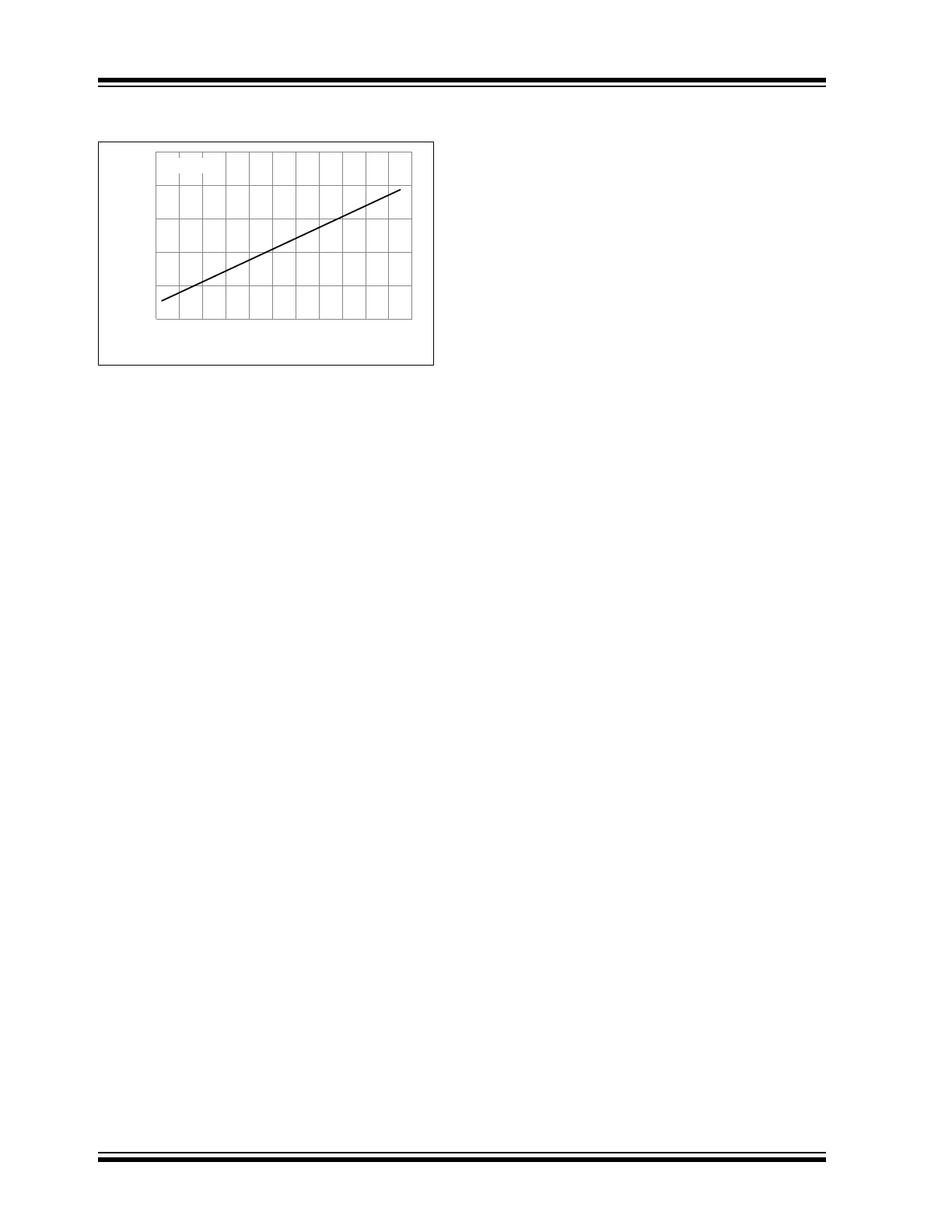
Note:
Unless otherwise indicated, T
A
= +25°C.
FIGURE 2-13:
Drain-to-Source Breakdown
Voltage vs. Temperature.
25
26
27
28
29
30
-60 -40 -20 0 20 40 60 80 100 120 140 160
V
BR(DSS)
- Breakdow
n V
oltage (V)
T
C
- Case Temperature(
°C)
I
D
= 250 µA
V
B
R
(D
SS)
-
B
reak
do
wn
V
o
lt
ag
e
(V
)

2012 Microchip Technology Inc.
DS25133B-page 7
MCP87022
3.0
PIN DESCRIPTIONS
The descriptions of the pins are listed in
Table 3-1
.
TABLE 3-1:
PIN FUNCTION TABLE
MCP87022
5x6 PDFN
Symbol
Description
1, 2, 3
S
Source pin
4
G
Gate pin
5, 6, 7, 8
D
Drain pin, including exposed thermal pad
MCP87022
DS25133B-page 8
2012 Microchip Technology Inc.
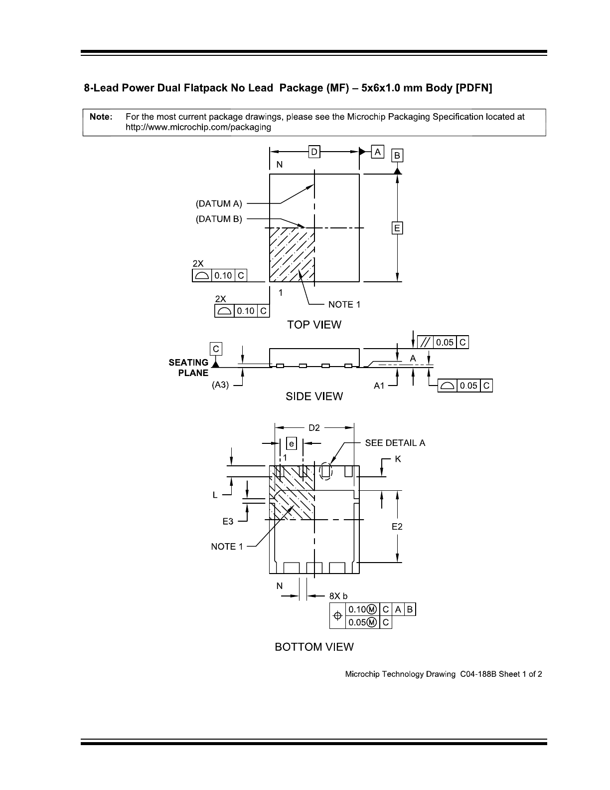
4.0
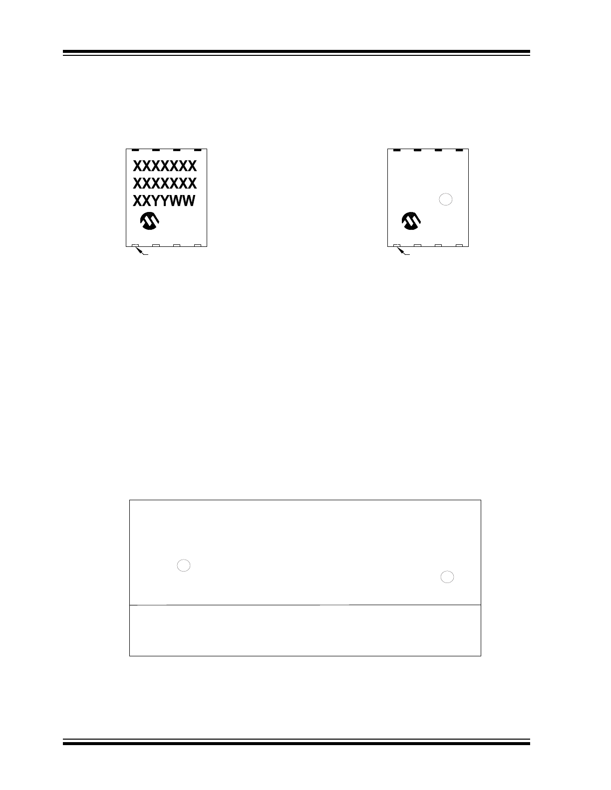
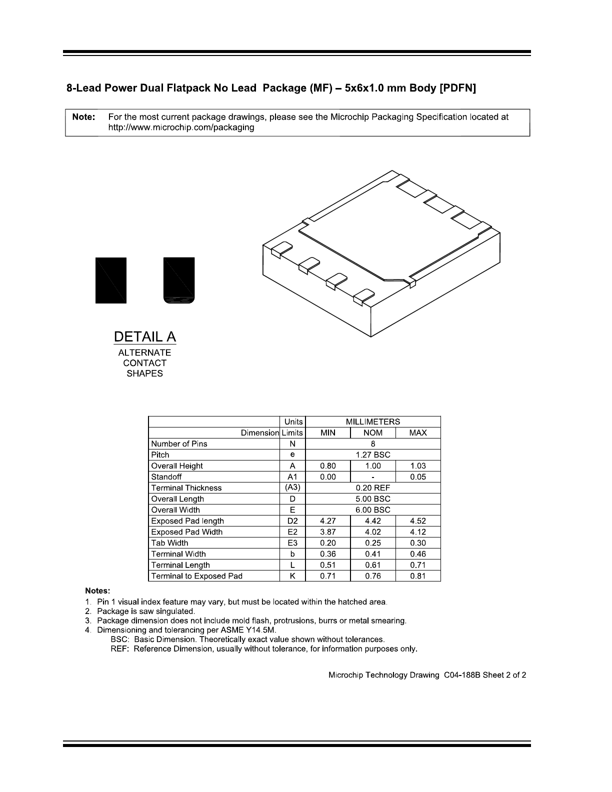
PACKAGING INFORMATION
4.1
Package Marking Information*
PIN 1
NNN
PIN 1
8-Lead PDFN (5x6x1.0 mm)
Example
Note
:
In the event the full Microchip part number cannot be marked on one line, it will
be carried over to the next line, thus limiting the number of available
characters for customer-specific information.
*RoHS compliant using EU-RoHS exemption: 7(a) - Lead in high-melting-temperature-type sol
ders
(i.e. lead-based alloys containing 85% by weight or more lead) can be found on the outer
packaging for this package.
Legend:
XX...X
Customer-specific information
Y
Year code (last digit of calendar year)
YY
Year code (last 2 digits of calendar year)
WW
Week code (week of January 1 is week ‘01’)
NNN
Alphanumeric traceability code
Pb-free JEDEC designator for Matte Tin (Sn)
*
This package is Pb-free. The Pb-free JEDEC designator ( )
can be found on the outer packaging for this package.
3
e
87022
U/MF ^^
1219
256
3
e
3
e
2012 Microchip Technology Inc.
DS25133B-page 9
MCP87022
MCP87022
DS25133B-page 10
2012 Microchip Technology Inc.