
2014 Microchip Technology Inc.
DS20005257B-page 1
Features
• Automotive AEC-Q100 Qualified, PPAP available
upon request
• Position Sensorless BLDC Drivers (no Hall
Sensor required)
• 180° Sinusoidal Drive for High Efficiency and Low
Acoustic Noise
• Supports 2V to 14V Power Supplies
• Speed Control through Power Supply Modulation
(PSM) and/or Pulse-Width Modulation (PWM)
• Built-In Frequency Generator (FG output signal)
• Built-In Lock-Up Protection and Automatic
Recovery Circuit (external capacitor not
necessary)
• Built-In Overcurrent Limitation (1.5A)
• Built-In Overvoltage Protection
• Built-In Thermal Shutdown Protection
• Thermally Enhanced 8-Lead 4 mm x 4 mm DFN
Package with Exposed Pad
• 23 kHz PWM Output Frequency
• No External Tuning Required
• Optimized for Fan Cooling Systems
Typical Applications
• Silent Notebook CPU/GPU Cooling Fans
• Air Ventilation System
• 12V 3-Phase BLDC Motors
Description
The MCP8063 device is a highly integrated 3-phase,
full-wave sensorless driver for brushless motors. It
features a 180° sinusoidal drive, high torque output,
and silent drive. Its integrated features and the wide
power supply range (2V to 14V) make the MCP8063 an
ideal candidate for a broad range of motor
characteristics, requiring no external tuning. Speed
control can be achieved through either power supply
modulation (PSM) or pulse-width modulation (PWM).
Due to the compact packaging and minimum bill of
materials (power transistors integrated, no Hall sensor,
no external tuning), the MCP8063 is optimized for fan
applications that require high efficiency and low
acoustic noise at competitive costs. Frequency
generator output enables precision speed control in
closed-loop applications. The MCP8063 driver
includes a Lock-Up Protection mode, which turns off
the output current when the motor is under lock
condition, and an automatic recovery that enables the
fan to restart when the lock condition is removed.
Features such as motor overcurrent limitation and
thermal shutdown protection improve motor system
reliability without additional efforts from design
engineers.
The MCP8063 is available in a compact
thermally-enhanced 8-lead 4 mm x 4 mm DFN
package with exposed pad.
Package Types
MCP8063
4x4 DFN*
* Includes Exposed Thermal Pad (EP); see
Table 3-1
.
Top View
OUT1
V
BIAS
OUT2
V
DD
OUT3
1
2
3
4
8
7
6
5 GND
PWM
FG
EP
9
3-Phase Brushless Sinusoidal Sensorless Motor Driver
MCP8063
MCP8063
DS20005257B-page 2
2014 Microchip Technology Inc.
Functional Block Diagram
Thermal
Protection
V
BIAS
OUT1
OUT2
MCU
PWM
FG
OUT3
V
DD
Ou
tp
u
t D
ri
v
e
C
ir
c
u
it
Motor Phase
Detection Circuit
Overcurrent
Limitation
PWM
Input
V
DD
Regulator
V
REF
GND
V
BIAS
2014 Microchip Technology Inc.
DS20005257B-page 3
MCP8063
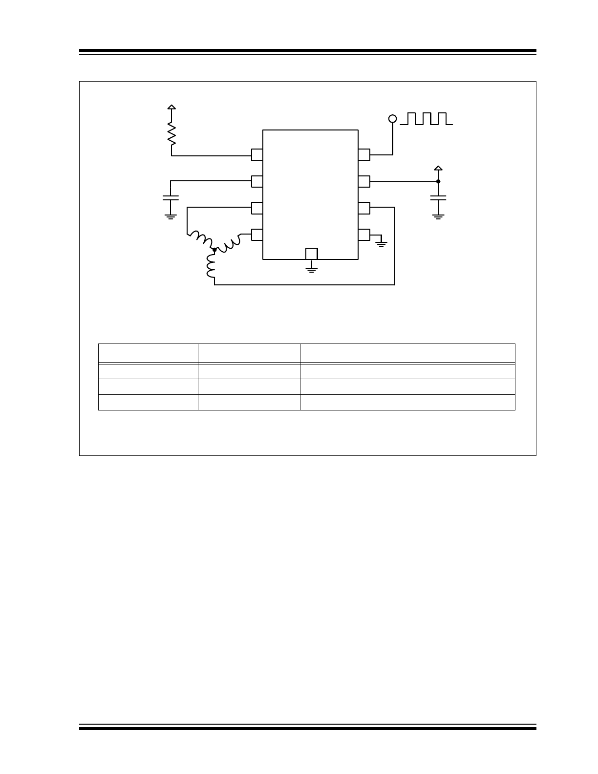
Typical Application – Fan Motor Driver Using the MCP8063
Recommended External Components for Typical Application
Element
Type/Value
Comment
C
1
≥1 µF
Connect as close as possible to IC input pins
C
2
≥10 µF
Connect as close as possible to IC input pins
R
1
≥10 kΩ
Connect to V
logic
on controller side
OUT1
FG
V
BIAS
OUT2
GND
V
DD
PWM
OUT3
1
2
3
4
5
6
7
8
MC
P
8
0
6
3
V
DD
PWM Input
(0.02-100 kHz)
C
1
C
2
R
1
V
LOGI C
(Controller Side)
9
EP

MCP8063
DS20005257B-page 4
2014 Microchip Technology Inc.
1.0
ELECTRICAL
CHARACTERISTICS
Absolute Maximum Ratings†
Power Supply Voltage (V
DD_MAX
) .................... -0.7 to +16.0V
Maximum OUT1,2,3 Voltage (V
OUT_MAX
) ........ -0.7 to +16.0V
Maximum Output Current
(
1
)
(I
OUT_MAX
) ...........-1.7A to +1.7A
FG Maximum Output Voltage (V
FG_MAX
) ......... -0.7 to +16.0V
FG Maximum Output Current (I
FG_MAX
)
.....................5.0 mA
V
BIAS
Maximum Voltage (V
BIAS_MAX
) ................ -0.7 to +4.0V
PWM Maximum Voltage (V
PWM_MAX
) ................ -0.7 to +4.0V
Maximum Junction Temperature (T
J
) .......................... +150°C
HBM ESD protection on all pins.......................................4 kV
† Notice:
Stresses above those listed under “Maximum
Ratings” may cause permanent damage to the device.
This is a stress rating only and functional operation of
the device at those or any other conditions above those
indicated in the operational listings of this specification
is not implied. Exposure to maximum rating conditions
for extended periods may affect device reliability.
Note 1:
OUT1, OUT2, OUT3 (Continuous,
100% duty cycle).
ELECTRICAL CHARACTERISTICS
Electrical Specifications:
Unless otherwise specified, all limits are established for V
DD
= 12.0V,
Temperature = +25°C.
Parameters
Sym.
Min.
Typ.
Max.
Units
Conditions
Power Supply Voltage
V
DD
2
—
14
V
Power Supply Current
I
VDD
—
—
10
—
—
mA
mA
Rotation Mode
5
Lock-Protection Mode
OUT1/2/3
High Resistance
R
ON(H)
—
0.6
1
Ω
I
OUT
= 0.5A, V
DD
= 3.3V to 14V
(
Note 1
)
OUT1/2/3
Low Resistance
R
ON(L)
—
0.6
1
Ω
I
OUT
= -0.5A, V
DD
= 3.3V to 14V
(
Note 1
)
OUT1/2/3
Total Resistance
R
ON(H+L)
—
1.2
2
Ω
I
OUT
= 0.5A, V
DD
= 3.3V to 14V
(
Note 1
)
OUT1/2/3 Maximum
Current Limitation
I
OUT_LIM
1.4
1.5
1.6
A
Note 1
V
BIAS
Output Voltage
V
BIAS
—
—
3
—
—
V
V
DD
= 3.3V to 14V
V
DD
– 0.2
V
V
DD
< 3.3V
PWM Input Frequency
f
PWM
0.02
—
100
kHz
PWM Input H Level
V
PWM_H
0.8 × V
BIAS
—
3.6
V
PWM Input L Level
V
PWM_L
0
—
0.2 × V
BIAS
V
PWM Internal Pull-Up
Current
I
PWM_L
17
34
—
µA
PWM = GND, V
DD
= 3.3V to 14V
8
17
—
µA
PWM = GND, V
DD
< 3.3V
PWM Output
Frequency
f
PWM_O
—
23
—
kHz
FG Output Pin Low
Level Voltage
V
OL_FG
—
—
0.25
V
I
FG
= -1 mA
FG Output Pin Leakage
Current
I
LH_FG
—
—
10
µA
V
FG
= 14V
Lock Protection
Operating Time
T
RUN
—
0.5
—
s
Lock Protection
Waiting Time
T
WAIT
4.0
4.5
5.0
s
Note 1:
Minimum and maximum parameter is not production tested and is specified by design and validation.
Reference PCB, according to JEDEC standard EIA/JESD 51-9.
2014 Microchip Technology Inc.
DS20005257B-page 5
MCP8063
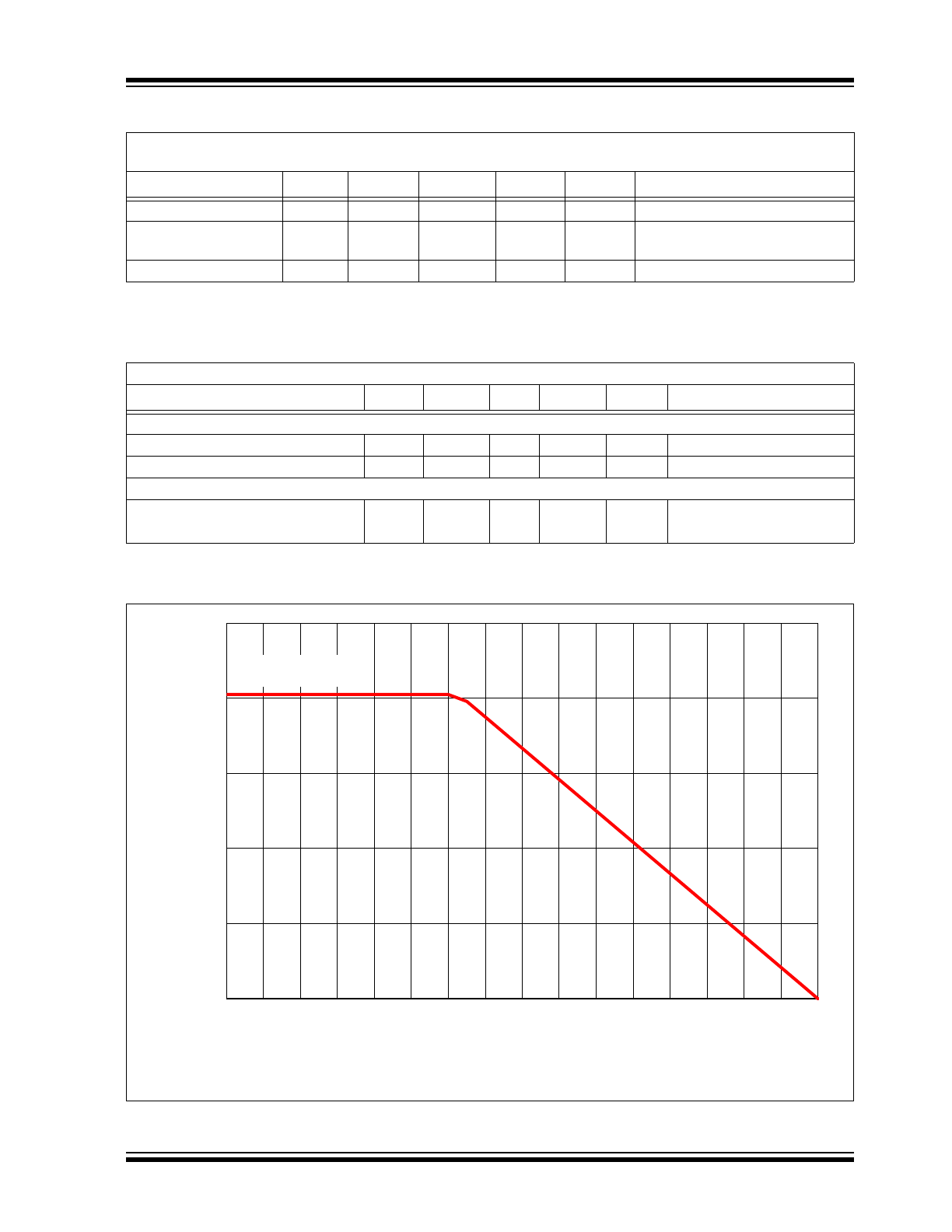
FIGURE 1-1:
Allowable Power Dissipation (P
D_MAX
) as a Function of Ambient Temperature (T
A
).
Thermal Shutdown
T
SD
—
170
—
°C
Thermal Shutdown
Hysteresis
T
SD_HYS
—
25
—
°C
Input Over Voltage
V
OV
—
18.5
—
V
TEMPERATURE SPECIFICATIONS
Electrical Specifications:
Unless otherwise specified, all limits are established for V
DD
= 12.0V, T
A
= +25°C.
Parameters
Sym.
Min.
Typ.
Max.
Units
Conditions
Temperature Ranges
Operating Temperature
T
OPR
-40
—
+125
°C
Storage Temperature Range
T
STG
-55
—
+150
°C
Package Thermal Resistances
Thermal Resistance, 8LD 4x4 DFN
JA
—
48
—
°C/W
JC
—
7
—
°C/W
Note 1:
Minimum and maximum parameter is not production tested and is specified by design and validation.
Derating applies for ambient temperatures outside the specified operating range (refer to
Figure 1-1
).
ELECTRICAL CHARACTERISTICS (CONTINUED)
Electrical Specifications:
Unless otherwise specified, all limits are established for V
DD
= 12.0V,
Temperature = +25°C.
Parameters
Sym.
Min.
Typ.
Max.
Units
Conditions
Note 1:
Minimum and maximum parameter is not production tested and is specified by design and validation.
Reference PCB, according to JEDEC standard EIA/JESD 51-9.
0
0.5
1
1.5
2
2.5
-10
0
10
20
30
40
50
60
70
80
90
100
11
0
120
130
140
150
P
DMA
X
(W)
T
A
(°C)
DFN-8
MCP8063
DS20005257B-page 6
2014 Microchip Technology Inc.
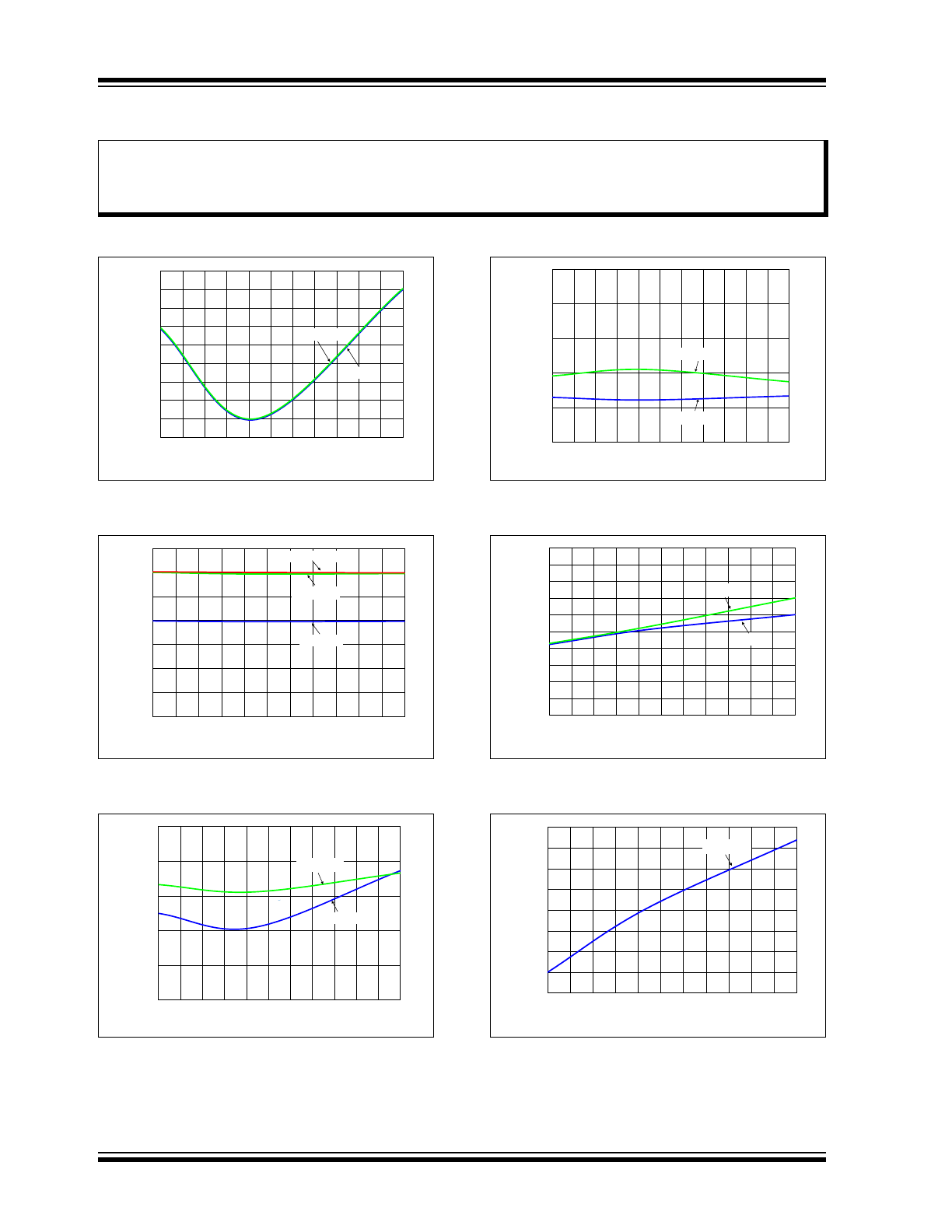
2.0
TYPICAL PERFORMANCE CURVES
Note:
Unless otherwise indicated, T
A
= +25°C, V
DD
= 14V, OUT1, 2, 3 and PWM open.
FIGURE 2-1:
Oscillator Frequency
Deviation vs. Temperature.
FIGURE 2-2:
Internal Regulated Voltage
(V
BIAS
) vs. Temperature.
FIGURE 2-3:
Input (PWM) V
IL
vs.
Temperature.
FIGURE 2-4:
Input (PWM) V
IH
vs.
Temperature.
FIGURE 2-5:
Output R
ON
Resistance vs.
Temperature (V
DD
= 3.3V).
FIGURE 2-6:
Supply Current vs.
Temperature.
Note:
The graphs and tables provided following this note are a statistical summary based on a limited number of
samples and are provided for informational purposes only. The performance characteristics listed herein
are not tested or guaranteed. In some graphs or tables, the data presented may be outside the specified
operating range (e.g., outside specified power supply range) and therefore outside the warranted range.
-2
0
2
4
6
8
10
12
14
16
-40 -25 -10
5
20 35 50 65 80 95 110 125
Oscillator Frequency
Deviation
(%
)
Temperature (C°)
V
DD
= 14V
V
DD
= 2V
0
0.5
1
1.5
2
2.5
3
3.5
-40 -25 -10
5
20
35
50
65
80
95 110 125
V
BIA
S
(V)
Temperature (C°)
V
DD
= 2V
V
DD
= 3.3V
V
DD
= 14V
25
30
35
40
45
50
-40 -25 -10
5
20
35
50
65
80
95 110 125
PWM V
IL
(%
of
V
BI
A
S
)
Temperature (C°)
V
DD
= 14V
V
DD
= 2V
50
55
60
65
70
75
-40 -25 -10
5
20
35
50
65
80
95 110 125
PWM V
IH
(%
of
V
BI
A
S
)
Temperature (C°)
V
DD
= 14V
V
DD
= 2V
0
0.1
0.2
0.3
0.4
0.5
0.6
0.7
0.8
0.9
1
-40 -25 -10
5
20
35
50
65
80
95 110 125
R
ON
(ȍ
)
Temperature (C°)
R
ON(H)
R
ON(L)
6.6
6.8
7
7.2
7.4
7.6
7.8
8
8.2
-40 -25 -10
5
20
35
50
65
80
95 110 125
I
VDD
Current (mA)
Temperature (C°)
V
DD
= 14V
2014 Microchip Technology Inc.
DS20005257B-page 7
MCP8063
Note:
Unless otherwise indicated, T
A
= +25°C, V
DD
= 14V, OUT1, 2, 3 and PWM open.
FIGURE 2-7:
FG Output Pin Low Level
Voltage (I
FG
= -1 mA).
FIGURE 2-8:
PWM Pull-Up Current vs.
Temperature.
FIGURE 2-9:
Typical Output on Start-Up.
FIGURE 2-10:
Typical Outputs on Closed
Loop.
FIGURE 2-11:
Typical Rotor Lock Situation.
0.04
0.05
0.06
0.07
0.08
0.09
0.1
0.11
0.12
-40 -25 -10
5
20 35 50 65 80 95 110 125
FG
Pin Drive (V)
Temperature (C°)
V
DD
= 3.3V
V
DD
= 2V
-40
-35
-30
-25
-20
-15
-10
-5
0
-40 -25 -10
5
20
35
50
65
80
95 110 125
PWM
Pull-Up Current (µA)
Temperature (C°)
V
DD
= 2V
V
DD
= 14V

MCP8063
DS20005257B-page 8
2014 Microchip Technology Inc.
3.0
PIN DESCRIPTIONS
The descriptions of the pins are listed in
Table 3-1
.
TABLE 3-1:
MCP8063 PIN FUNCTION TABLE
MCP8063
Symbol
Type
Description
4x4 DFN
1
FG
O
Motor Speed Indication Output Pin
2
V
BIAS
P
Internal Regulator Output Pin (for decoupling only)
3
OUT1
O
Single-Phase Coil Output Pin
4
OUT2
O
Single-Phase Coil Output Pin
5
GND
P
Negative Voltage Supply Pin (Ground)
6
OUT3
O
Single-Phase Coil Output Pin
7
V
DD
P
Positive Voltage Supply for Motor Driver Pin
8
PWM
I
PWM Input Signal for Speed Control Pin
9
EP
P
Exposed pad is used for thermal dissipation. Connect to GND.
Legend:
I = Input; O = Output; P = Power
2014 Microchip Technology Inc.
DS20005257B-page 9
MCP8063
4.0
FUNCTIONAL DESCRIPTION
The MCP8063 device generates a full-wave signal to
drive a 3-phase sensorless BLDC motor. High
efficiency and low power consumption are achieved
due to DMOS transistors and synchronous rectification
drive type. The current carrying order of the output is as
follows: OUT1
OUT2 OUT3.
4.1
Speed Control
The rotational speed of the motor can be controlled
either through the PWM digital input signal or by
varying the power supply (V
DD
). When the PWM signal
is “High” (or left open), the motor rotates at full speed.
When the PWM signal is “Low”, the motor is stopped
(and the driver outputs are set to high impedance). By
changing the PWM duty cycle, the speed can be
adjusted. Notice that the PWM frequency has no
special meaning for the motor speed and is
asynchronous with the activation of the output
transistors. Thus, the user has maximum freedom to
choose the PWM system frequency within a wide range
(from 20 Hz to 100 kHz), while the output transistor
activation always occurs at a fixed rate, which is
outside the range of audible frequencies. The typical
output frequency of MCP8063 is 23 kHz.
4.2
Frequency Generator Function
The Frequency Generator output is a “Hall-sensor
equivalent” digital output, giving information to an
external controller about the speed and phase of the
motor. The FG pin is an open-drain output, connecting
to a logical voltage level through an external pull-up
resistor. When a lock (or out-of-sync) situation is
detected by the driver, this output is set to high
impedance until the motor is restarted. Leave the pin
open when not used. The FG signal can be used to
compute the motor speed in rotations per minute
(RPM). Typically, for a four-pole BLDC fan (4P/6S), the
speed in RPMs is 30 x FG frequency (Hz).
EQUATION 1-1:
4.3
Lock-Up Protection and Automatic
Restart
If the motor is stopped (blocked) or if it loses
synchronization with the driver, a lock-up protection
circuit detects this situation and ties the outputs to GND
in order to dissipate the remaining energy from the
rotor with a minimum of self heating. After a “waiting
time” (T
WAIT
), the lock-up protection is released and
normal operation resumes for a given time (T
RUN
). In
case the motor is still blocked, a new period of waiting
time is started. T
WAIT
and T
RUN
timings are fixed
internally, so that no external capacitor is needed.
4.4
Overcurrent Limitation
The motor peak current is limited by the driver to a fixed
value (defined internally), thus limiting the maximum
power dissipation in the coils.
4.5
Thermal Shutdown
The MCP8063 device has a thermal protection function
which detects when the die temperature exceeds
T
SD
= +170°C. When this temperature is reached, the
circuit enters Thermal Shutdown mode and the outputs
OUT1, OUT2 and OUT3 are tied to GND in order to
dissipate the remaining energy from the rotor with a
minimum of self-heating. Once the junction
temperature (T
SD
) has dropped below +145°C, the
normal operation resumes (the thermal detection
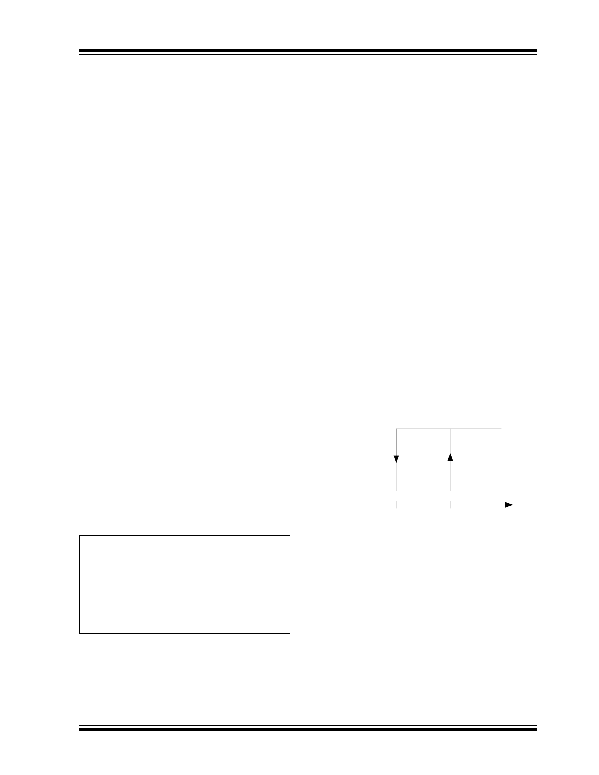
circuit has +25°C hysteresis function).
FIGURE 4-1:
Thermal Protection
Hysteresis.
4.6
Internal Voltage Regulator
V
BIAS
voltage is generated internally and is used to
supply internal logical blocks. The V
BIAS
pin is used to
connect an external decoupling capacitor (1 µF or
higher). Notice that this pin is for IC internal use and is
not designed to supply DC current to external blocks.
4.7
Overvoltage Shutdown
The MCP8063 device has an overvoltage protection
function which detects when the V
DD
voltage exceeds
V
OV
= +18.5V. When this temperature is reached, the
circuit enters Thermal Shutdown mode, and outputs
OUT1, OUT2 and OUT3 are disabled (high impedance).
FG
720
P
S
-----------------------
Where:
P =
Total number of poles in the motor
S =
Total number of slots in the motor
= Rotor speed RPM
T
SD
+145°C
Thermal Shutdown
+170°C
Normal operation
MCP8063
DS20005257B-page 10
2014 Microchip Technology Inc.
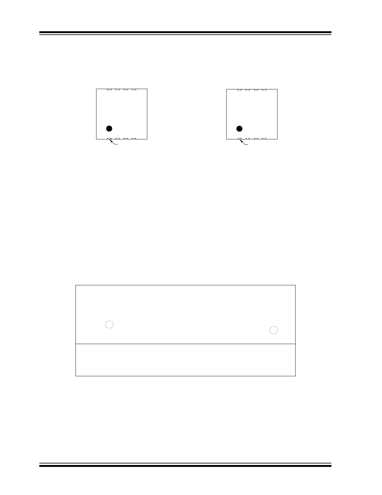
5.0
PACKAGING INFORMATION
5.1
Package Marking Information
Legend:
XX...X
Customer-specific information
Y
Year code (last digit of calendar year)
YY
Year code (last 2 digits of calendar year)
WW
Week code (week of January 1 is week ‘01’)
NNN
Alphanumeric traceability code
Pb-free JEDEC
®
designator for Matte Tin (Sn)
*
This package is Pb-free. The Pb-free JEDEC designator ( )
can be found on the outer packaging for this package.
Note
:
In the event the full Microchip part number cannot be marked on one line, it will
be carried over to the next line, thus limiting the number of available
characters for customer-specific information.
3
e
3
e
8-Lead DFN (4x4x0.9 mm)
Example
YYWW
NNN
XXXXXX
XXXXXX
PIN 1
PIN 1
8063
300EMD
1442
256