
2008-2018 Microchip Technology Inc.
DS20002090D-page 1
MCP73871
Features
• Integrated System Load Sharing and Battery
Charge Management
- Simultaneously Power the System and
Charge the Li-Ion Battery
- Voltage Proportional Current Control (VPCC)
ensures system load has priority over Li-Ion
battery charge current
- Low-Loss Power-Path Management with
Ideal Diode Operation
• Complete Linear Charge Management Controller
- Integrated Pass Transistors
- Integrated Current Sense
- Integrated Reverse Discharge Protection
- Selectable Input Power Sources: USB Port or
AC-DC Wall Adapter
• Preset High Accuracy Charge Voltage Options:
- 4.10V, 4.20V, 4.35V or 4.40V
- ±0.5% Regulation Tolerance
• Constant Current/Constant Voltage (CC/CV)
Operation with Thermal Regulation
• Maximum 1.8A Total Input Current Control
• Resistor Programmable Fast Charge Current
Control: 50 mA to 1A
• Resistor Programmable Termination Set Point
• Selectable USB Input Current Control
- Absolute Maximum: 100 mA (L)/500 mA (H)
• Automatic Recharge
• Automatic End-of-Charge Control
• Safety Timer With Timer Enable/Disable Control
• 0.1C Preconditioning for Deeply Depleted Cells
• Battery Cell Temperature Monitor
• Undervoltage Lockout (UVLO)
• Low Battery Status Indicator (LBO)
• Power Good Status Indicator (PG)
• Charge Status and Fault Condition Indicators
• Numerous Selectable Options Available for a
Variety of Applications:
- Refer to
Section 1.0 “Electrical
Characteristics”
for Selectable Options
- Refer to the
Product Identification System
for Standard Options
• Temperature Range: -40°C to +85°C
• Packaging: 20-Lead QFN (4 mm x 4 mm)
Applications
• GPSs/Navigators
• PDAs and Smart Phones
• Portable Media Players and MP3 Players
• Digital Cameras
• Bluetooth
®
Headsets
• Portable Medical Devices
• Charge Cradles/Docking Stations
• Toys
Description
The MCP73871 device is a fully integrated linear
solution for system load sharing and Li-Ion/Li-Polymer
battery charge management with AC-DC wall adapter
and USB port power sources selection. It is also
capable of autonomous power source selection
between input and battery. Along with its small physical
size, the low number of required external components
makes the device ideally suited for portable
applications.
The MCP73871 device automatically obtains power for
the system load from a single-cell Li-Ion battery or an
input power source (AC-DC wall adapter or USB port).
The MCP73871 device specifically adheres to the
current drawn limits governed by the USB specification.
With an AC-DC wall adapter providing power to the
system, an external resistor sets the magnitude of 1A
maximum charge current while supporting up to 1.8A
total current for system load and battery charge
current.
The MCP73871 device employs a constant
current/constant voltage (CC/CV) charge algorithm
with selectable charge termination point. To
accommodate new and emerging battery charging
requirements, the constant voltage regulation is fixed
with four available options: 4.10V, 4.20V, 4.35V or
4.40V. The MCP73871 device also limits the charge
current based on the die temperature during high
power or high ambient conditions. This thermal
regulation optimizes the charge cycle time while
maintaining device reliability.
The MCP73871 device includes a low battery indicator,
a power good indicator and two charge status
indicators that allow for outputs with LEDs or
communication with host microcontrollers. The
MCP73871 device is fully specified over the ambient
temperature range of -40°C to +85°C.
Stand-Alone System Load Sharing and Li-Ion/Li-Polymer Battery Charge
Management Controller
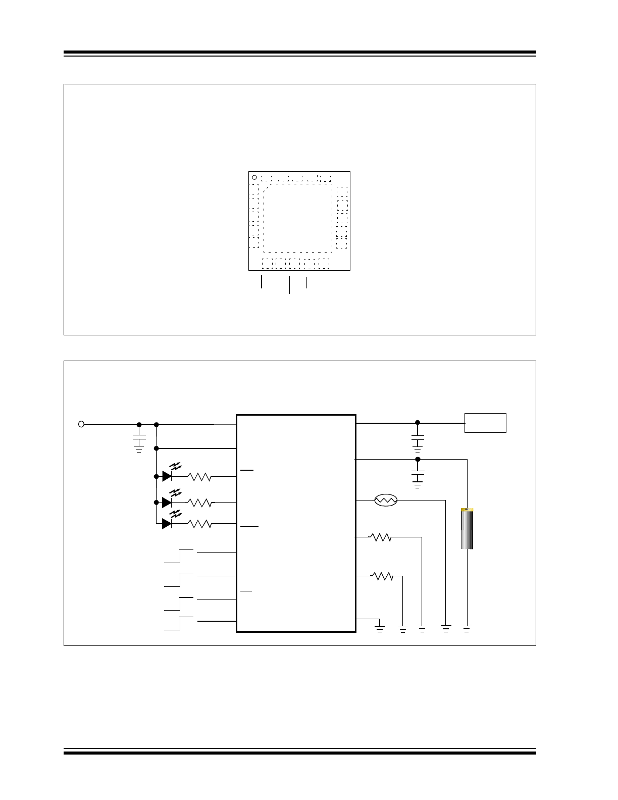
MCP73871
DS20002090D-page 2
2008-2018 Microchip Technology Inc.
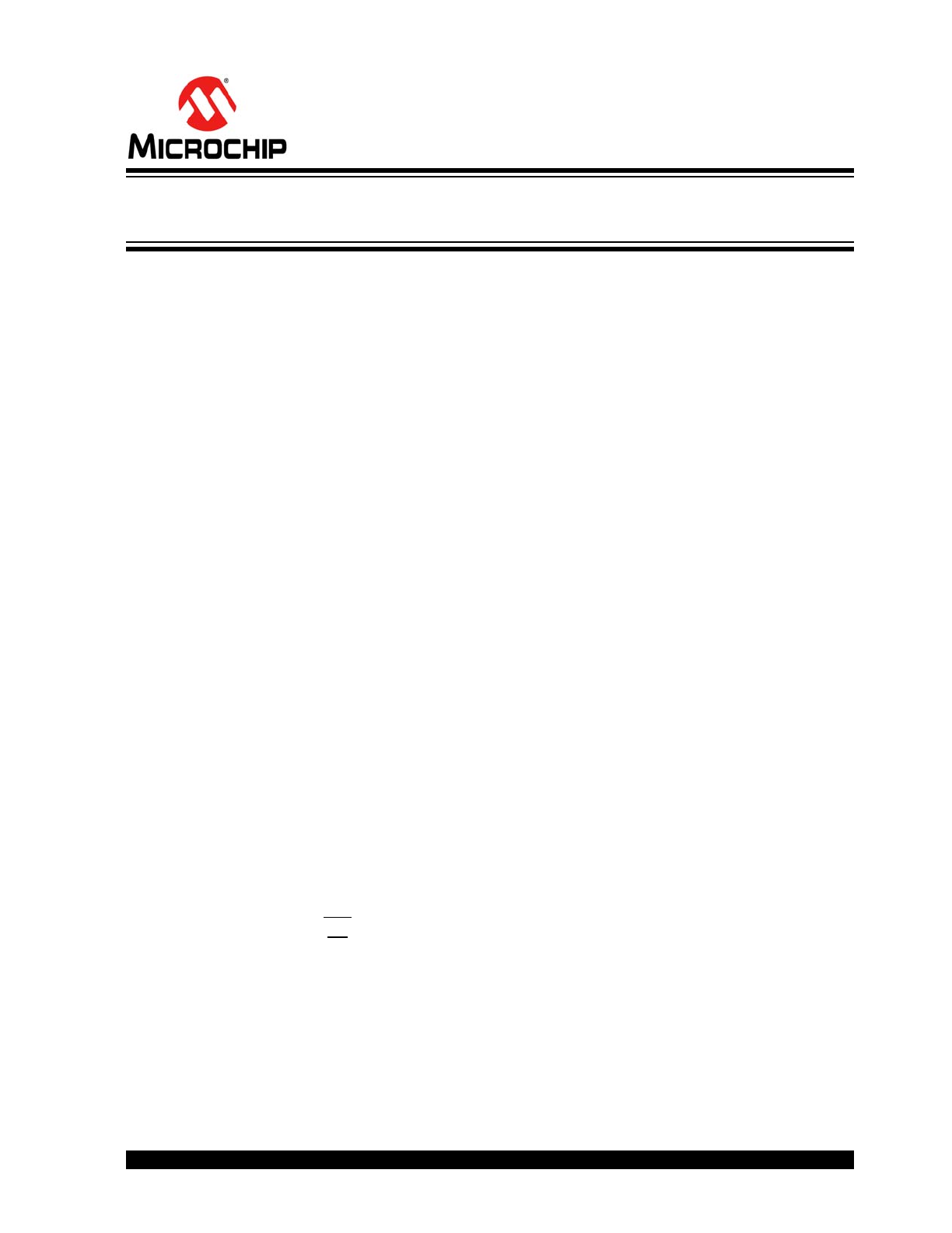
Package Types
Typical Application Circuit
IN
S
TA
T1/
L
BO
PG
THERM
ST
A
T
2
PROG1
IN
OUT
OUT
CE
SEL
PROG3
TE
V
BAT
V
BAT
VPCC
V
SS
V
SS
V
BA
T
_SEN
SE
2
EP
20
1
19 18 17
3
4
12
11
10
9
5
6
7
8
13
14
15
16
21
PROG2
MCP73871
20-Lead QFN*
* Includes Exposed Thermal Pad (EP); see
Table 3-1
.
STAT1
LBO
IN
OUT
PG
V
BAT
Single-Cell
Li-Ion Battery
7
1, 20
8
18, 19
10 µF
10, 11, EP
AC-DC Adapter
or
USB Port
STAT2
THERM
V
SS
PROG1
PROG3 12
13 R
PROG1
6
5
14, 15, 16
470
470
470
2
4.7 µF
System
Load
SEL
TE
PROG2
Hi
Low
Hi
Low
Hi
Low
3
4
9
R
PROG3
VPCC
NTC
10 k
Hi
Low
17
CE
4.7 µF
MCP73871 Typical Application
2008-2018 Microchip Technology Inc.
DS20002090D-page 3
MCP73871
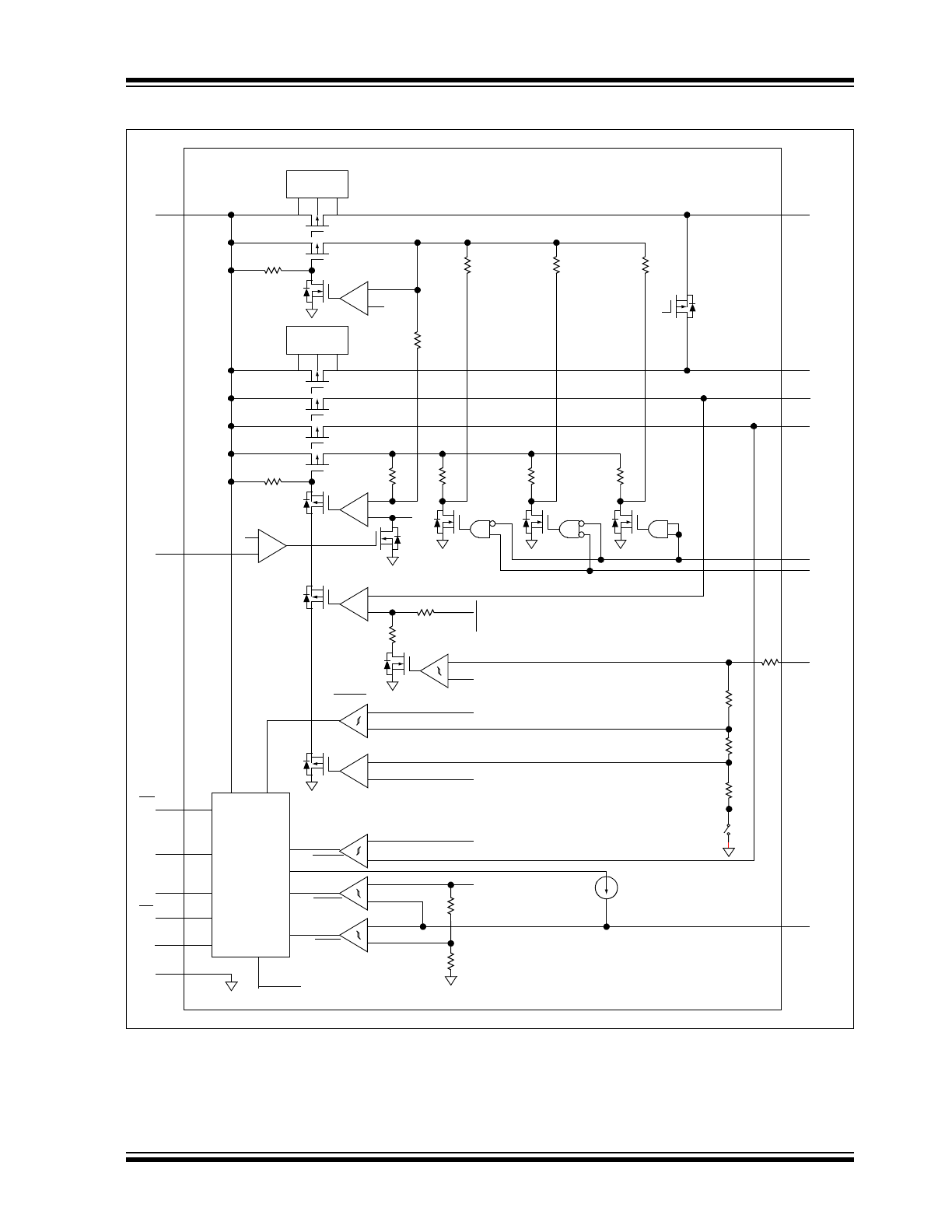
Functional Block Diagram
STAT1
PROG1
V
BAT
G = 0.001
V
SS
Direction
Control
TERM
+
-
+
-
LTVT
+
-
HTVT
THERM
50 µA
UVLO,
REFERENCE,
CHARGE
CONTROL,
TIMER,
AND
STATUS
LOGIC
STAT2
PG
Direction
Control
PROG2
IN
+
-
CURRENT
LIMIT
V
REF
+
-
CURRENT
LIMIT
V
REF
/2
PROG3
+
-
CA
V
REF
PRECONDITION
+
-
V
REF
+
-
VA
V
REF
V
REF
SEL
OUT
V
REF
TE
0.2
0.2
Ideal
Diode,
Synchronous
Switch
CHRG
+
-
V
REF
+
-
V
REF
VPCC
CE
V
BAT_SENSE
G = 0.001
G = 0.001
G = 0.001
V
REF
(1.21V)
361k
190k
7k
89k

MCP73871
DS20002090D-page 4
2008-2018 Microchip Technology Inc.
NOTES:
2008-2018 Microchip Technology Inc.
DS20002090D-page 5
MCP73871
1.0
ELECTRICAL
CHARACTERISTICS
Absolute Maximum Ratings†
V
I
N
....................................................................................7.0V
All Inputs and Outputs w.r.t. ................ V
SS
-0.3V to V
DD
+0.3V
(V
DD
= V
IN
or V
BAT
)
Maximum Junction Temperature, T
J
............ Internally Limited
Storage temperature .....................................-65°C to +150°C
ESD protection on all pins
Human Body Model (1.5 k
in Series with 100 pF) 4 kV
Machine Model (200 pF, No Series Resistance) .............300V
† Notice: Stresses above those listed under “Maximum
Ratings” may cause permanent damage to the device.
This is a stress rating only and functional operation of
the device at those or any other conditions above those
indicated in the operational listings of this specification
is not implied. Exposure to maximum rating conditions
for extended periods may affect device reliability.
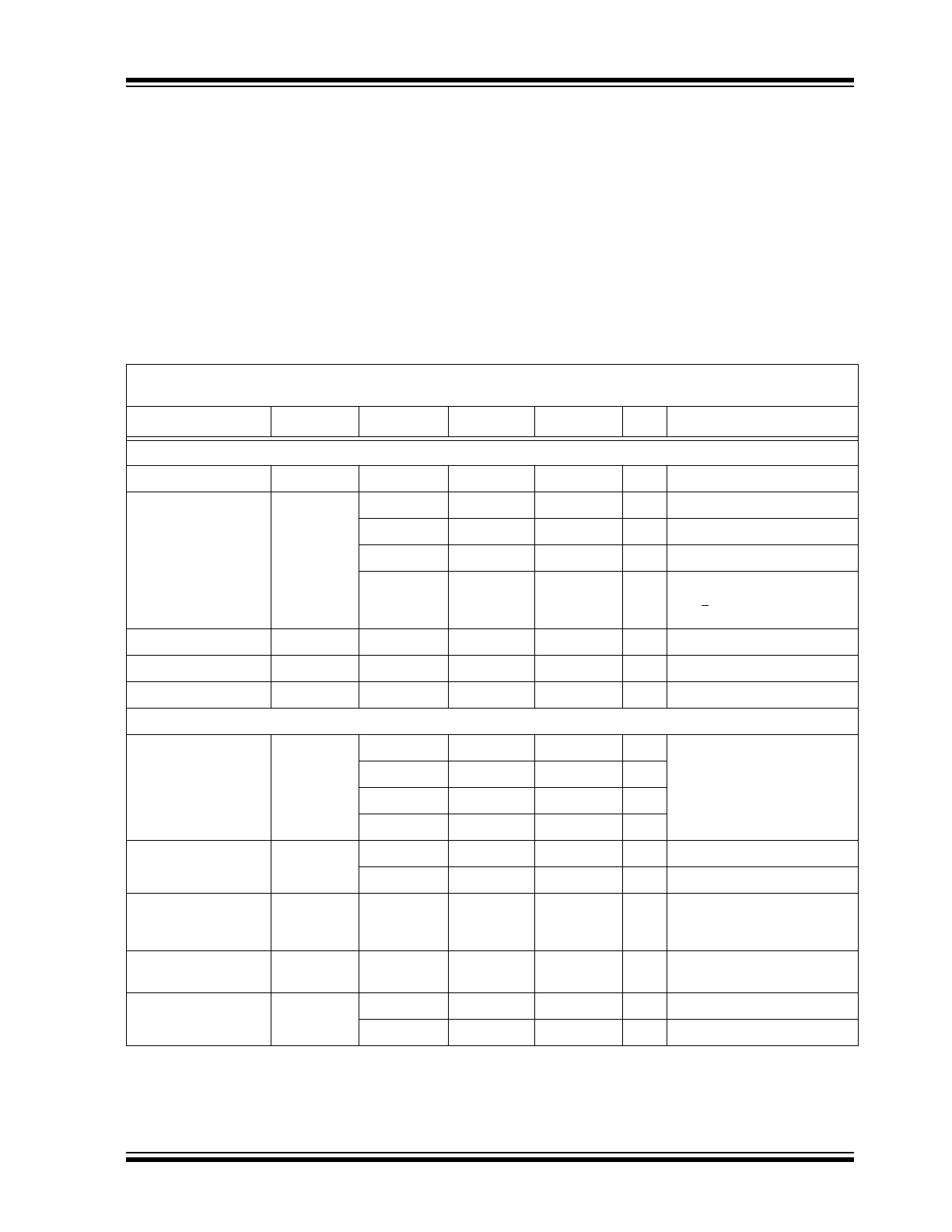
DC CHARACTERISTICS
Electrical Specifications: Unless otherwise indicated, all limits apply for V
IN
= V
REG
+ 0.3V to 6V, T
A
= -40°C to +85°C.
Typical values are at +25°C, V
IN
= [V
REG
(typical) + 1.0V]
Parameters
Sym
Min
Typ
Max
Units
Conditions
Supply Input
Supply Voltage
V
IN
V
REG
+ 0.3V
—
6
V
Supply Current
I
SS
—
2500
3750
µA
Charging
—
260
350
µA
Charge Complete
—
180
300
µA
Standby
—
28
50
µA
Shutdown
(V
DD
< V
BAT
– 100 mV or
V
DD
< V
STOP
)
UVLO Start Threshold
V
START
V
REG
+ 0.05V V
REG
+ 0.15V V
REG
+ 0.25V
V
V
DD
= Low-to-High
UVLO Stop Threshold
V
STOP
V
REG
– 0.07V V
REG
+ 0.07V V
REG
+ 0.17V
V
V
DD
= High-to-Low
UVLO Hysteresis
V
HYS
—
90
—
mV
Voltage Regulation (Constant Voltage Mode)
Regulated
Charge Voltage
V
REG
4.080
4.10
4.121
V
V
DD
= [V
REG
(typical) + 1V]
I
OUT
= 10 mA
T
A
= -5°C to +55°C
4.179
4.20
4.221
V
4.328
4.35
4.372
V
4.378
4.40
4.422
Regulated Charge
Voltage Tolerance
V
RTOL
-0.5
—
+0.5
%
T
A
= +25°C
-0.75
—
+0.75
%
T
A
= -5°C to +55°C
Line Regulation
V
BAT
/V
BAT
)
/
V
DD
|
—
0.08
0.20
%/V
V
DD
= [V
REG
(typical) + 1V] to 6V
I
OUT
= 10 mA
Load Regulation
V
BAT
/V
BAT
|
—
0.08
0.18
%
I
OUT
= 10 mA to 150 mA
V
DD
= [V
REG
(typical) + 1V]
Supply Ripple
Attenuation
PSRR
—
-47
—
dB
I
OUT
= 10 mA, 1 kHz
—
-40
—
dB
I
OUT
= 10 mA, 10 kHz
Note 1:
The value is ensured by design and not production tested.
2:
The maximum available charge current is also limited by the value set at PROG1 input.
MCP73871
DS20002090D-page 6
2008-2018 Microchip Technology Inc.
Current Regulation (Fast Charge Constant Current Mode)
AC-Adapter
Fast Charge
Current
I
REG
90
100
110
mA
PROG1 = 10 k
T
A
= -5°C to +55°C, SEL = High
900
1000
1100
mA
PROG1 = 1 k
T
A
= -5°C to +55°C, SEL = High
USB Fast Charge
Current
I
REG
80
90
100
mA
PROG2 = Low, SEL = Low,
(
Note 2
)
T
A
= -5°C to +55°C
400
450
500
mA
PROG2 = High, SEL = Low,
(
Note 2
)
T
A
= -5°C to +55°C
Input Current Limit Control (ICLC)
USB-Port Supply
Current Limit
I
LIMIT_USB
80
90
100
mA
PROG2 = Low, SEL = Low
T
A
= -5°C to +55°C
400
450
500
mA
PROG2 = High, SEL = Low
T
A
= -5°C to +55°C
AC-DC Adapter Current
Limit
I
LIMIT_AC
1500
1650
1800
mA
SEL = High, T
A
= -5°C to +55°C
Voltage Proportional Charge Control (VPCC - Input Voltage Regulation)
VPCC Input Threshold
V
VPCC
—
1.23
—
V
I
OUT
= 10 mA
T
A
= -5°C to +55°C
VPCC Input Threshold
Tolerance
V
RTOL
-3
—
+3
%
Input Leakage Current
I
LK
—
0.01
1
µA
V
VPCC
= V
DD
Precondition Current Regulation (Trickle Charge Constant Current Mode)
Precondition Current
Ratio
I
PREG
/I
REG
7.5
10
12.5
%
PROG1 = 1.0 k
to 10 k
T
A
= -5°C to +55°C
Precondition Current
Threshold Ratio
V
PTH
/V
REG
69
72
75
%
V
BAT
Low-to-High
Precondition Hysteresis
V
PHYS
—
105
—
mV
V
BAT
High-to-Low
Automatic Charge Termination Set Point
Charge Termination
Current Ratio
I
TERM
75
100
125
mA
PROG3 = 10 k
T
A
= -5°C to +55°C
7.5
10
12.5
mA
PROG3 = 100 k
T
A
= -5°C to +55°C
Automatic Recharge
Recharge Voltage
Threshold Ratio
V
RTH
V
REG
– 0.21V V
REG
– 0.15V V
REG
– 0.09V
V
V
BAT
High-to-Low
IN-to-OUT Pass Transistor ON-Resistance
ON-Resistance
R
DS_ON
—
200
—
m
V
DD
= 4.5V, T
J
= 105°C
DC CHARACTERISTICS (CONTINUED)
Electrical Specifications: Unless otherwise indicated, all limits apply for V
IN
= V
REG
+ 0.3V to 6V, T
A
= -40°C to +85°C.
Typical values are at +25°C, V
IN
= [V
REG
(typical) + 1.0V]
Parameters
Sym
Min
Typ
Max
Units
Conditions
Note 1:
The value is ensured by design and not production tested.
2:
The maximum available charge current is also limited by the value set at PROG1 input.
2008-2018 Microchip Technology Inc.
DS20002090D-page 7
MCP73871
Charge Transistor ON-Resistance
ON-Resistance
R
DSON_
—
200
—
m
V
DD
= 4.5V, T
J
= 105°C
BAT-to-OUT Pass Transistor ON-Resistance
ON-Resistance
R
DS_ON
—
200
—
m
V
DD
= 4.5V, T
J
= 105°C
Battery Discharge Current
Output Reverse
Leakage Current
I
DISCHARGE
—
30
40
µA
Shutdown
(V
BAT
< V
DD
< V
UVLO
)
—
30
40
µA
Shutdown (0 < V
DD
< V
BAT
)
—
30
40
µA
V
BAT
= Power Out, No Load
—
-6
-13
µA
Charge Complete
Status Indicators - STAT1 (LBO), STAT2, PG
Sink Current
I
SINK
—
16
35
mA
Low Output Voltage
V
OL
—
0.4
1
V
I
SINK
= 4 mA
Input Leakage Current
I
LK
—
0.01
1
µA
High Impedance, V
DD
on pin
Low Battery Indicator (LBO)
Low Battery Detection
Threshold
V
LBO
—
Disable
—
V
BAT
> V
IN
, PG = Hi-Z
T
A
= -5°C to +55°C
2.85
3.0
3.15
V
2.95
3.1
3.25
V
3.05
3.2
3.35
V
Low Battery Detection
Hysteresis
V
LBO_HYS
—
150
—
mV
V
BAT
Low-to-High
PROG1 Input (PROG1)
Charge Impedance
Range
R
PROG
1
—
20
k
PROG3 Input (PROG3)
Termination Impedance
Range
R
PROG
5
—
100
k
PROG2 Input (PROG2)
Input High Voltage Level
V
IH
1.8
—
—
V
Input Low Voltage Level
V
IL
—
—
0.8
V
Input Leakage Current
I
LK
—
0.01
1
µA
V
PROG2
= V
DD
Timer Enable (TE)
Input High Voltage Level
V
IH
1.8
—
—
V
Note 1
Input Low Voltage Level
V
IL
—
—
0.8
V
Note 1
Input Leakage Current
I
LK
—
0.01
1
µA
V
TE
= V
DD
DC CHARACTERISTICS (CONTINUED)
Electrical Specifications: Unless otherwise indicated, all limits apply for V
IN
= V
REG
+ 0.3V to 6V, T
A
= -40°C to +85°C.
Typical values are at +25°C, V
IN
= [V
REG
(typical) + 1.0V]
Parameters
Sym
Min
Typ
Max
Units
Conditions
Note 1:
The value is ensured by design and not production tested.
2:
The maximum available charge current is also limited by the value set at PROG1 input.
MCP73871
DS20002090D-page 8
2008-2018 Microchip Technology Inc.
Chip Enable (CE)
Input High Voltage Level
V
IH
1.8
—
—
V
Input Low Voltage Level
V
IL
—
—
0.8
V
Input Leakage Current
I
LK
—
0.01
1
µA
V
CE
= V
DD
Input Source Selection (SEL)
Input High Voltage Level
V
IH
1.8
—
—
V
Input Low Voltage Level
V
IL
—
—
0.8
V
Input Leakage Current
I
LK
—
0.01
1
µA
V
SEL
= V
DD
Thermistor Bias
Thermistor Current
Source
I
THERM
47
50
53
µA
2 k
< R
THERM
< 50 k
Thermistor Comparator
Upper Trip Threshold
V
T1
1.20
1.24
1.26
V
V
T1
Low-to-High
Upper Trip Point
Hysteresis
V
T1HYS
—
-40
—
mV
Lower Trip Threshold
V
T2
0.23
0.25
0.27
V
V
T2
High-to-Low
Lower Trip Point
Hysteresis
V
T2HYS
—
40
—
mV
Thermal Shutdown
Die Temperature
T
SD
—
150
—
C
Die Temperature
Hysteresis
T
SDHYS
—
10
—
C
DC CHARACTERISTICS (CONTINUED)
Electrical Specifications: Unless otherwise indicated, all limits apply for V
IN
= V
REG
+ 0.3V to 6V, T
A
= -40°C to +85°C.
Typical values are at +25°C, V
IN
= [V
REG
(typical) + 1.0V]
Parameters
Sym
Min
Typ
Max
Units
Conditions
Note 1:
The value is ensured by design and not production tested.
2:
The maximum available charge current is also limited by the value set at PROG1 input.
2008-2018 Microchip Technology Inc.
DS20002090D-page 9
MCP73871
AC CHARACTERISTICS
Electrical Specifications: Unless otherwise indicated, all limits apply for V
IN
= 4.6V to 6V.
Typical values are at +25°C, V
DD
= [V
REG
(typical) + 1.0V]
Parameters
Sym
Min
Typ
Max
Units
Conditions
UVLO Start Delay
t
START
—
—
5
ms
V
DD
Low-to-High
Current Regulation
Transition Time Out of Precondition
t
DELAY
—
—
10
ms
V
BAT
< V
PTH
to V
BAT
> V
PTH
Current Rise Time Out of Precondition
t
RISE
—
—
10
ms
I
OUT
Rising to 90% of I
REG
Precondition Comparator Filter Time
t
PRECON
0.4
1.3
3.2
ms
Average V
BAT
Rise/Fall
Termination Comparator Filter Time
t
TERM
0.4
1.3
3.2
ms
Average I
OUT
Falling
Charge Comparator Filter Time
t
CHARGE
0.4
1.3
3.2
ms
Average V
BAT
Falling
Thermistor Comparator Filter Time
t
THERM
0.4
1.3
3.2
ms
Average THERM Rise/Fall
Elapsed Timer
Elapsed Timer Period
t
ELAPSED
—
0
—
Hours
3.6
4.0
4.4
Hours
5.4
6.0
6.6
Hours
7.2
8.0
8.8
Hours
Status Indicators
Status Output Turn-off
t
OFF
—
—
500
µs
I
SINK
= 1 mA to 0 mA
Status Output Turn-on
t
ON
—
—
500
µs
I
SINK
= 0 mA to 1 mA
Note 1:
Internal safety timer is tested based on internal oscillator frequency measurement.
TEMPERATURE SPECIFICATIONS
Electrical Specifications: Unless otherwise indicated, all limits apply for V
IN
= 4.6V to 6V.
Typical values are at +25°C, V
DD
= [V
REG
(typical) + 1.0V]
Parameters
Sym
Min
Typ
Max
Units
Conditions
Temperature Ranges
Specified Temperature Range
T
A
-40
—
+85
°C
Operating Temperature Range
T
J
-40
—
+125
°C
Storage Temperature Range
T
A
-65
—
+150
°C
Thermal Package Resistances
Thermal Resistance, 20LD-QFN, 4x4
JA
—
50
—
°C/W
4-Layer JC51-7 Standard Board,
Natural Convection
JC
—
8
—
—

MCP73871
DS20002090D-page 10
2008-2018 Microchip Technology Inc.
NOTES: