
2007-2015 Microchip Technology Inc.
DS20002071C-page 1
MCP73837/8
Features
• Highly Accurate Preset Voltage Regulation:
±0.5%
• Available Voltage Regulation Options:
- 4.20V, 4.35V, 4.4V or 4.5V
• Complete Linear Charge Management Controller:
- Autonomous Power Source Selection
- Integrated Pass Transistors
- Integrated Current Sense
- Integrated Reverse Discharge Protection
• Constant Current (CC)/Constant Voltage (CV)
Operation with Thermal Regulation
• Selectable USB Port Charge Current:
- Low: 1 Unit Load
- High: 5 Unit Loads
• Programmable AC Adapter Charge Current:
- 15 mA – 1000 mA
• Two-Charge Status Outputs
• Power-Good Monitor: MCP73837
• Timer Enable: MCP73838
• Automatic Recharge:
- Selectable Voltage Threshold
• Automatic End-of-Charge Control:
- Selectable Charge Termination Current Ratio
- Selectable Safety Timer Period
• Preconditioning of Deeply Depleted Cells – Can
Be Disabled
• Battery Cell Temperature Monitor
• UVLO (Undervoltage Lockout)
• Automatic Power-Down When Input Power Is
Removed
• Low-Dropout (LDO) Linear Regulator Mode
• Numerous Selectable Options Available for a
Variety of Applications:
- Refer to
Section 1.0 “Electrical Characteris-
tics”
for Selectable Options
- Refer to the “
Product Identification System
”
for Standard Options
• Temperature Range: -40°C to 85°C
• Packaging:
- 10-Lead 3 mm x 3 mm DFN
- 10-Lead MSOP*
* Consult the factory for MSOP availability.
Applications
• Smart Phones and Personal Data Assistants
(PDA)
• Portable Media Players (PMP)
• Ultra Mobile Devices (UMD)
• Digital Cameras
• MP3 Players
• Bluetooth Headsets
• Handheld Medical Devices
• AC/USB Dual Source Li-Ion Battery Chargers
Description
The MCP73837 and MCP73838 devices are fully
integrated linear Li-Ion/Li-Polymer battery chargers
with autonomous power source selection. Along with its
small physical size, the low number of external
components required makes the MCP73837/8 ideally
suitable for portable applications.
The MCP73837/8 automatically selects the USB port or
AC adapter as the power source for the system. For the
USB port powered systems, the MCP73837/8
specifically adheres to the current limits governed by
the USB specification. The host microcontroller can
select from two preset maximum charge current rates
of 100 mA (low-power USB port) or 500 mA
(high-power USB port). With an AC adapter providing
power to the system, an external resistor sets the mag-
nitude of the system or charge current up to a
maximum of 1A.
The MCP73837/8 employs a constant current/constant
voltage charge algorithm with selectable
preconditioning and charge termination. The constant
voltage regulation is fixed with four available options:
4.20V, 4.35V, 4.40V or 4.50V, to accommodate the new
emerging battery charging requirements. The
MCP73837/8 limits the charge current, based on die
temperature, during high power or high ambient
conditions. This thermal regulation optimizes the
charge cycle time while maintaining the reliability of the
device .
The MCP73837/8 are fully specified over the ambient
temperature range of -40°C to +85°C.
The MCP73837/8 devices are available in either a
3 mm x 3 mm 10-lead DFN package or a 10-lead
MSOP package.
Advanced Stand-Alone Li-Ion/Li-Polymer Battery Charge
Management Controller with Autonomous AC Adapter or
USB Port Source Selection
MCP73837/8
DS20002071C-page 2
2007-2015 Microchip Technology Inc.
Package Types
Typical Applications
2
3
4
5
6
7
8
9
PROG2
V
SS
V
USB
STAT1
PG (TE)
THERM
3 x 3 10-Lead DFN*
MCP73837/8
STAT2
1
10 V
BAT
V
AC
PROG1
6
7
8
9
PROG2
V
SS
V
USB
STAT1
PG (TE)
THERM
10-Lead MSOP
MCP73837/8
STAT2
10 V
BAT
V
AC
PROG1
1
2
3
4
5
EP
11
*Includes Exposed Thermal Pad (EP); see
Table 3-1
.
STAT1
V
AC
V
SS
PG
V
BAT
Single
Li-Ion
Cell
4
MCP73837 Typical Application
5
3
1
4.7 µF
2
AC/DC Adapter
STAT2
THERM
V
USB
PROG1
PROG2
USB Port
6
7
Hi
Low
Thermistor
R
PROG
8
9
10
1 k
1 k
1 k
STAT1
V
AC
V
SS
TE
V
BAT
Cell
4
MCP73838 Typical Application
5
3
1
2
AC/DC Adapter
STAT2
THERM
V
USB
PROG1
PROG2
USB Port
6
7
Hi
Low
Thermistor
8
9
10
Hi
Low
1 K
1 K
4.7 µF
4.7 µF
4.7 µF
4.7 µF
4.7 µF
R
PROG
2007-2015 Microchip Technology Inc.
DS20002071C-page 3
MCP73837/8
Functional Block Diagram (MCP73837/8)
Reference,
Bias, UVLO,
and SHDN
V
REF
(1.21V)
STAT1
PROG1
V
BAT
SENSEFET
G = 0.001
Vss
Direction
Control
175k
+
-
Precondition
+
-
TERM
+
-
111k
+
-
CA
10k
157.3k
6k
48k
470.6k
CHARGE
+
-
+
-
VA
72.7k
310k
1k
+
-
Current
Limit
+
-
LTVT
+
-
HTVT
470.6k
121k
THERM
ȝ$
Charge Control,
Timer,
and
Status Logic
STAT2
PG (TE)
LDO
1M
175k
Direction
Control
ȝ$
10k
2k
100mA/500mA
SENSEFET
G = 0.001
SENSEFET
G = 0.001
SENSEFET
G = 0.001
V
REF
AC/USB
AC/USB
VO
REG
VO
REG
VO
REG
UVLO
VO
REG
PROG2
V
AC
V
USB
MCP73837/8
DS20002071C-page 4
2007-2015 Microchip Technology Inc.
1.0
ELECTRICAL
CHARACTERISTICS
Absolute Maximum Ratings†
V
DDN
.................................................................................7.0V
All Inputs and Outputs w.r.t. V
SS
............. -0.3 to (V
DD
+ 0.3)V
Maximum Junction Temperature, T
J
............Internally Limited
Storage temperature .....................................-65°C to +150°C
ESD protection on all pins
Human Body Model (1.5 k
in Series with 100 pF) ...... ≥4 kV
Machine Model (200 pF, No Series Resistance) .............300V
† Notice: Stresses above those listed under “Maximum
Ratings” may cause permanent damage to the device. This is
a stress rating only and functional operation of the device at
those or any other conditions above those indicated in the
operational listings of this specification is not implied.
Exposure to maximum rating conditions for extended periods
may affect device reliability.
DC CHARACTERISTICS
Electrical Specifications: Unless otherwise indicated, all limits apply for V
DD
= [V
REG
(typical) + 0.3V] to 6V, T
A
= -40°C to +85°C.
Typical values are at +25°C, V
DD
= [V
REG
(typical) + 1.0V].
Parameters
Sym.
Min.
Typ.
Max.
Units
Conditions
Supply Input
Supply Voltage
V
DD
V
REG
(Typ)
+0.3V
—
6
V
(
1
)
Supply Current
I
SS
—
1900
3000
µA
Charging
—
—
110
300
µA
Charge Complete, No Battery
75
100
µA
Standby (PROG Floating)
0.6
5
µA
Shutdown (V
DD
≤ V
BAT –
100 mV
or V
DD
< V
STOP
)
UVLO Start Threshold
V
START
3.35
3.45
3.55
V
V
DD
= Low to High (USB Port)
UVLO Stop Threshold
V
STOP
3.25
3.35
3.45
V
V
DD
= High to Low (USB Port)
UVLO Hysteresis
V
HYS
—
75
—
mV
(USB Port)
UVLO Start Threshold
V
START
4.1
4.15
4.3
V
(AC Adapter)
UVLO Stop Threshold
V
STOP
4.0
4.1
4.2
V
(AC Adapter)
UVLO Hysteresis
V
HYS
—
55
—
mV
(AC Adapter)
Voltage Regulation (Constant Voltage Mode)
Regulated Charge Voltage
V
REG
4.179
4.20
4.221
V
V
DD
= [V
REG
(typical) + 1V]
—
4.328
4.35
4.372
V
I
OUT
= 30 mA
4.378
4.40
4.422
V
T
A
= -5°C to +55°C
4.477
4.50
4.523
V
Regulated Charge Voltage
Tolerance
V
RTOL
-0.5
—
+0.5
%
T
A
= -5°C to +55°C
Line Regulation
V
BAT
/V
BAT
)
/
V
DD
|
—
0.075
0.2
%/V
V
DD
= [V
REG
(typical)+1V] to 6V
I
OUT
= 30 mA
Load Regulation
V
BAT
/V
BAT
|
—
0.150
0.3
%
I
OUT
= 10 mA to 100 mA
V
DD
= [V
REG
(typical)+1V]
Supply Ripple Attenuation
PSRR
—
60
—
dB
I
OUT
= 10 mA, 10Hz to 1 kHz
—
—
52
—
dB
I
OUT
= 10 mA, 10Hz to 10 kHz
—
23
—
dB
I
OUT
= 10 mA, 10Hz to 1 MHz
Current Regulation (Fast Charge Constant-Current Mode)
AC Adapter Fast Charge Current
I
REG
95
105
115
mA
PROG1 = 10 k
—
900
1000
1100
mA
PROG1 = 1 k
(
2
)
T
A
= -5°C to +55°C
Note 1:
The supply voltage (V
DD
) = V
AC
when input power source is from AC adapter and the supply voltage (V
DD
) = V
USB
when input power source is from the USB port.
2:
The value is guaranteed by design and not production tested.
3:
The current is based on the ratio of selected current regulation (I
REG
).
The maximum charge impedance has to be less than shutdown impedance for normal operation.
2007-2015 Microchip Technology Inc.
DS20002071C-page 5
MCP73837/8
USB port Fast Charge Current
I
REG
80
90
100
mA
PROG2 = Low
—
400
450
500
mA
PROG2 = High
T
A
= -5°C to +55°C
Maximum Output Current Limit
I
MAX
—
1200
—
mA
PROG1 < 833
Precondition Current Regulation (Trickle Charge Constant-Current Mode)
Precondition Current Ratio
I
PREG
/I
REG
7.5
10
12.5
%
(
3
)
—
15
20
25
%
T
A
= -5°C to +55°C
30
40
50
%
—
100
—
%
Precondition Current Threshold
Ratio
V
PTH
/V
REG
64
66.5
69
%
V
BAT
Low to High
—
69
71.5
74
%
Precondition Hysteresis
V
PHYS
—
120
—
mV
V
BAT
High to Low
Charge Termination
Charge Termination Current Ratio
I
TERM
/I
REG
3.75
5
6.25
%
PROG1 = 1 k
to 10 k
—
5.6
7.5
9.4
%
T
A
= -5°C to +55°C
7.5
10
12.5
%
(
3
)
15
20
25
%
Automatic Recharge
Recharge Voltage Threshold Ratio
V
RTH
/V
REG
92
94.0
96
%
V
BAT
High to Low
—
95
97
99
%
T
A
= -5°C to +55°C
Pass Transistor ON-Resistance
ON-Resistance
R
DSON
—
350
—
m
V
DD
= 4.5V, T
J
= +105°C
Battery Discharge Current
Output Reverse Leakage Current
I
DISCHARGE
—
0.1
2
µA
Standby (PROG1 or PROG2
Floating)
—
—
0.55
2
µA
Shutdown (V
DD
≤ V
BAT
-100 mV
or V
DD
< V
STOP
)
—
-6
-15
µA
Charge Complete
Status Indicators – STAT1, STAT2, PG (MCP73837)
Sink Current
I
SINK
—
16
35
mA
Low Output Voltage
V
OL
—
0.3
1
V
I
SINK
= 4 mA
Input Leakage Current
I
LK
—
0.03
1
µA
High Impedance, V
DD
on pin
PROG1 Input (PROG1)
Charge Impedance Range
R
PROG
1
—
—
k
(
4
)
Shutdown Impedance
R
PROG
70
—
200
k
Minimum Impedance for
Shutdown
PROG2 Inputs (PROG2)
Input High Voltage Level
V
IH
0.8V
DD
—
—
%
Input Low Voltage Level
V
IL
—
—
0.2V
DD
%
Shutdown Voltage Level
V
SD
0.2V
DD
—
0.8V
DD
%
Input Leakage Current
I
LK
—
7
15
µA
V
PROG2
= V
DD
DC CHARACTERISTICS (Continued)
Electrical Specifications: Unless otherwise indicated, all limits apply for V
DD
= [V
REG
(typical) + 0.3V] to 6V, T
A
= -40°C to +85°C.
Typical values are at +25°C, V
DD
= [V
REG
(typical) + 1.0V].
Parameters
Sym.
Min.
Typ.
Max.
Units
Conditions
Note 1:
The supply voltage (V
DD
) = V
AC
when input power source is from AC adapter and the supply voltage (V
DD
) = V
USB
when input power source is from the USB port.
2:
The value is guaranteed by design and not production tested.
3:
The current is based on the ratio of selected current regulation (I
REG
).
The maximum charge impedance has to be less than shutdown impedance for normal operation.
MCP73837/8
DS20002071C-page 6
2007-2015 Microchip Technology Inc.
Timer Enable (TE)
Input High Voltage Level
V
IH
2
—
—
V
Input Low Voltage Level
V
IL
—
—
0.8
V
Input Leakage Current
ILK
—
0.01
1
µA
V
TE
= V
DD
Thermistor Bias
Thermistor Current Source
I
THERM
47
50
53
µA
2 k
< R
THERM
< 50 k
Thermistor Comparator
Upper Trip Threshold
V
T1
1.20
1.23
1.26
V
V
T1
Low to High
Upper Trip Point Hysteresis
V
T1HYS
—
-40
—
mV
Lower Trip Threshold
V
T2
0.235
0.250
0.265
V
V
T2
High to Low
Lower Trip Point Hysteresis
V
T2HYS
—
40
—
mV
System Test (LDO) Mode
Input High Voltage Level
V
IH
—
—
V
DD
– 0.1
V
THERM Input Sink Current
I
SINK
3
5.5
20
µA
Stand-by or System Test Mode
Bypass Capacitance
C
BAT
1
4.7
—
—
µF
µF
I
OUT
< 250 mA
I
OUT
> 250 mA
Automatic Power Down (SLEEP Comparator, Direction Control)
Automatic Power Down Entry
Threshold
V
PD
V
BAT
+
10 mV
V
BAT
+
100 mV
—
V
2.3V ≤ V
BAT
≤ V
REG
V
DD
Falling
Automatic Power Down Exit
Threshold
V
PDEXIT
—
V
BAT
+
150 mV
V
BAT
+
250 mV
V
2.3V ≤ V
BAT
≤ V
REG
V
DD
Rising
Thermal Shutdown
Die Temperature
T
SD
—
150
—
C
Die Temperature Hysteresis
T
SDHYS
—
10
—
C
DC CHARACTERISTICS (Continued)
Electrical Specifications: Unless otherwise indicated, all limits apply for V
DD
= [V
REG
(typical) + 0.3V] to 6V, T
A
= -40°C to +85°C.
Typical values are at +25°C, V
DD
= [V
REG
(typical) + 1.0V].
Parameters
Sym.
Min.
Typ.
Max.
Units
Conditions
Note 1:
The supply voltage (V
DD
) = V
AC
when input power source is from AC adapter and the supply voltage (V
DD
) = V
USB
when input power source is from the USB port.
2:
The value is guaranteed by design and not production tested.
3:
The current is based on the ratio of selected current regulation (I
REG
).
The maximum charge impedance has to be less than shutdown impedance for normal operation.
2007-2015 Microchip Technology Inc.
DS20002071C-page 7
MCP73837/8
AC CHARACTERISTICS
TEMPERATURE SPECIFICATIONS
Electrical Specifications: Unless otherwise indicated, all limits apply for V
DD
= [V
REG
(typical) + 0.3V] to 6V.
Typical values are at +25°C, V
DD
= [V
REG
(typical) + 1.0V] .
Parameters
Sym.
Min.
Typ.
Max.
Units
Conditions
UVLO Start Delay
t
START
—
—
5
ms
V
DD
Low to High
Current Regulation
Transition Time Out of Precondition
t
DELAY
—
—
10
ms
V
BAT
< V
PTH
to V
BAT
> V
PTH
Current Rise Time Out of Precondition
t
RISE
—
—
10
ms
I
OUT
Rising to 90% of I
REG
Precondition Comparator Filter Time
t
PRECON
0.4
1.3
3.2
ms
Average V
BAT
Rise/Fall
Termination Comparator Filter Time
t
TERM
0.4
1.3
3.2
ms
Average I
OUT
Falling
Charge Comparator Filter Time
t
CHARGE
0.4
1.3
3.2
ms
Average V
BAT
Falling
Thermistor Comparator Filter Time
t
THERM
0.4
1.3
3.2
ms
Average THERM Rise/Fall
Elapsed Timer
Elapsed Timer Period
t
ELAPSED
0
0
0
Hours
Timer Disabled
—
3.6
4.0
4.4
Hours
—
5.4
6.0
6.6
Hours
—
7.2
8.0
8.8
Hours
Status Indicators
Status Output Turn-off
t
OFF
—
—
500
µs
I
SINK
= 1 mA to 0 mA
Status Output Turn-on
t
ON
—
—
500
µs
I
SINK
= 0 mA to 1 mA
Electrical Specifications: Unless otherwise indicated, all limits apply for V
DD
= [V
REG
(typ.) + 0.3V] to 6V.
Typical values are at +25°C, V
DD
= [V
REG
(typ.) + 1.0V] .
Parameters
Sym.
Min.
Typ.
Max.
Units
Conditions
Temperature Ranges
Specified Temperature Range
T
A
-40
—
+85
°C
Operating Temperature Range
T
J
-40
—
+125
°C
Storage Temperature Range
T
A
-65
—
+150
°C
Thermal Package Resistances
Thermal Resistance, 10-Lead MSOP
JA
—
113
—
°C/W
4-Layer JC51-7 Standard Board,
Natural Convection
(
1
)
Thermal Resistance, 10-Lead 3 x 3 DFN
JA
—
41
—
°C/W
4-Layer JC51-7 Standard Board,
Natural Convection
Note 1:
This represents the minimum copper condition on the Printed Circuit Board (PCB).
MCP73837/8
DS20002071C-page 8
2007-2015 Microchip Technology Inc.
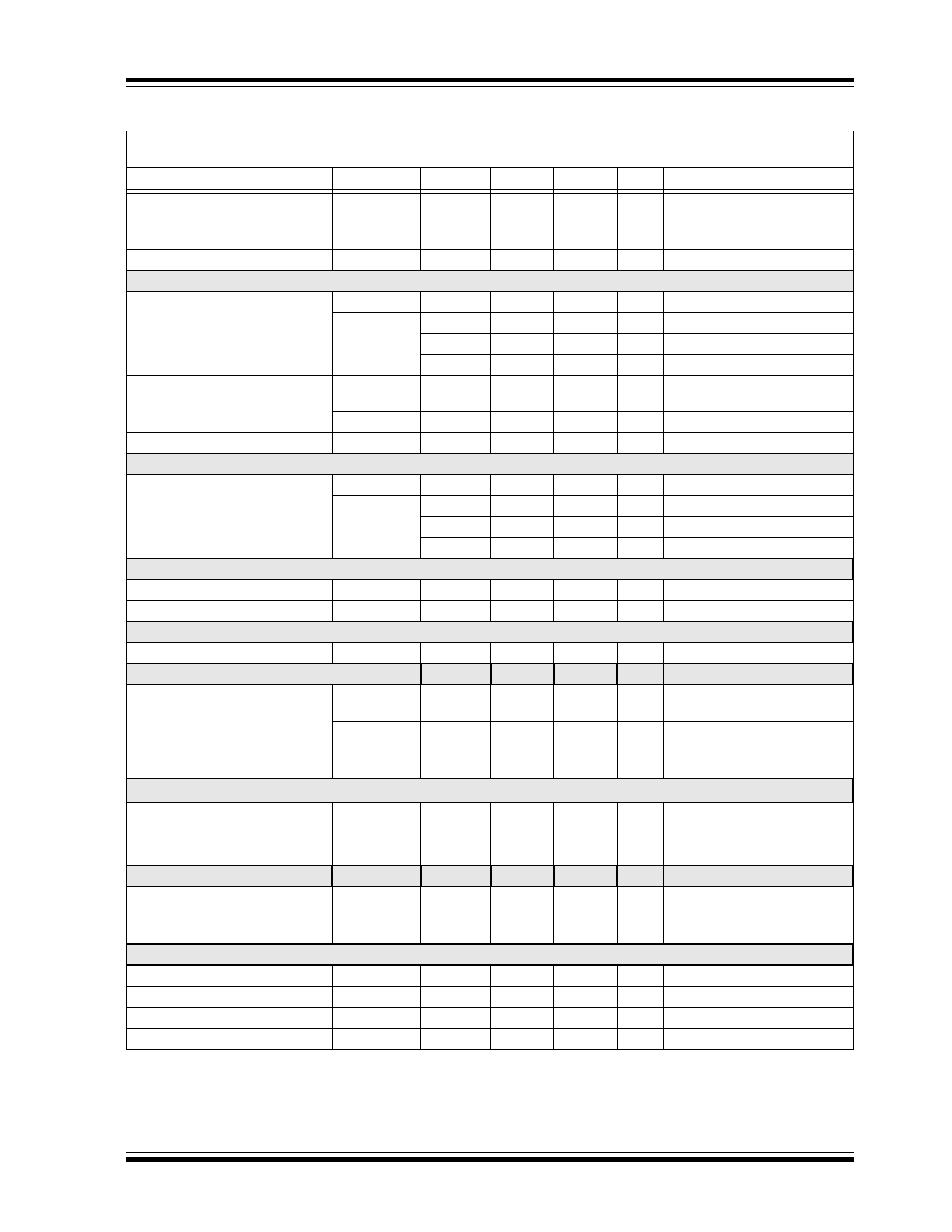
2.0
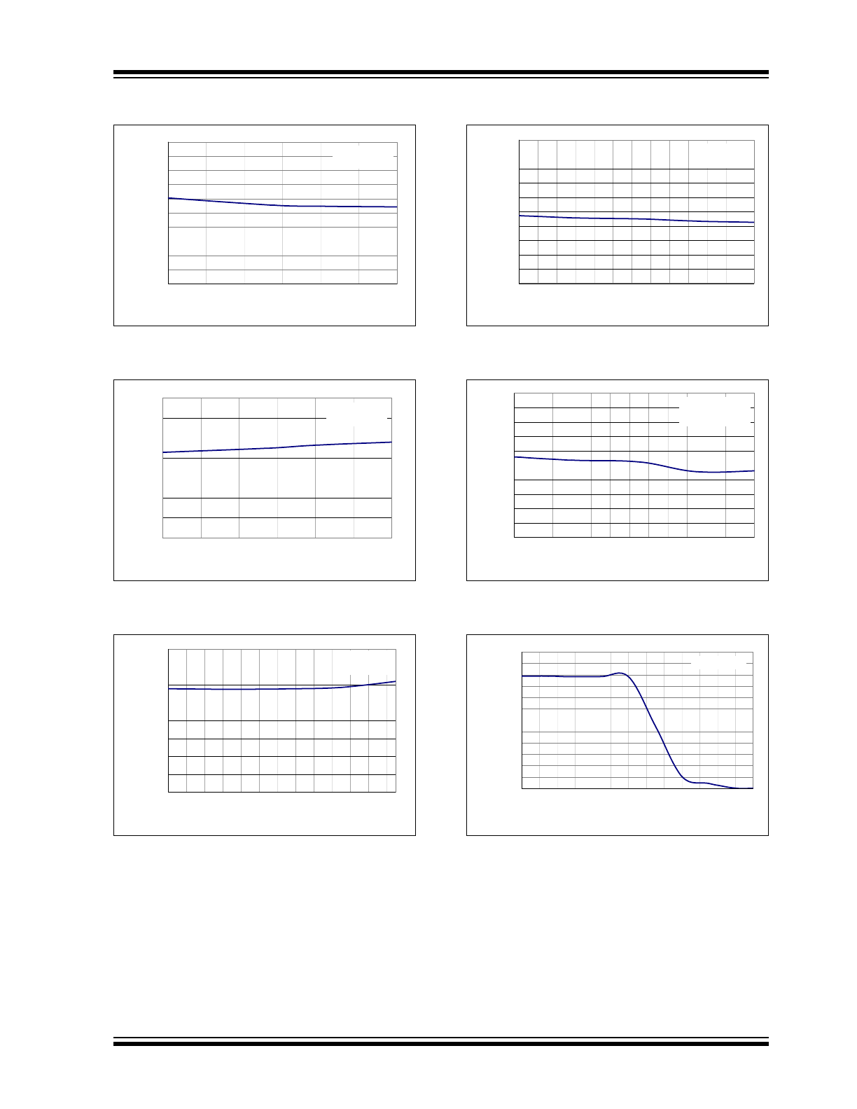
TYPICAL PERFORMANCE CURVES
Note: Unless otherwise indicated, V
DD
= [V
REG
(typical) + 1V], I
OUT
= 30 mA, and T
A
= +25°C, Constant-voltage mode.
FIGURE 2-1:
Battery Regulation Voltage
(V
BAT
) vs. Supply Voltage (V
DD
).
FIGURE 2-2:
Battery Regulation Voltage
(V
BAT
) vs. Ambient Temperature (T
A
).
FIGURE 2-3:
Output Leakage Current
(I
DISCHARGE
) vs. Battery Regulation Voltage
(V
BAT
).
FIGURE 2-4:
Output Leakage Current
(I
DISCHARGE
) vs. Ambient Temperature (T
A
).
FIGURE 2-5:
Output Leakage Current
(I
DISCHARGE
) vs. Battery Voltage (V
BAT
).
FIGURE 2-6:
Charge Current (I
OUT
) vs.
Programming Resistor (R
PROG
).
Note:
The graphs and tables provided following this note are a statistical summary based on a limited number of
samples and are provided for informational purposes only. The performance characteristics listed herein
are not tested or guaranteed. In some graphs or tables, the data presented may be outside the specified
operating range (e.g., outside specified power supply range) and therefore outside the warranted range.
4.160
4.165
4.170
4.175
4.180
4.185
4.190
4.195
4.200
4.205
4.210
4.5
4.8
5.0
5.3
5.5
5.8
6.0
Supply Voltage (V)
B
at
ter
y R
eg
u
la
ti
o
n
V
o
lt
ag
e
(
V
)
TEMP = 25°C
I
OUT
= 10 mA
I
OUT
= 100 mA
I
OUT
= 500 mA
I
OUT
= 1000 mA
I
OUT
= 50 mA
4.170
4.175
4.180
4.185
4.190
4.195
4.200
4.205
4.210
-40 -30 -20 -10 0 10 20 30 40 50 60 70 80
Ambient Temperature (°C)
Bat
tery
Reg
u
lat
io
n
V
o
lt
ag
e (
V
)
I
OUT
= 10 mA
V
DD
= 5.2V
I
OUT
= 1000 mA
I
OUT
= 500 mA
I
OUT
= 100 mA
I
OUT
= 50 mA
0.00
0.05
0.10
0.15
0.20
0.25
0.30
0.35
0.40
0.45
0.50
3.0 3.1 3.2 3.3 3.4 3.5 3.6 3.7 3.8 3.9 4.0 4.1 4.2
Battery Voltage (V)
Out
put
Le
ak
ag
e Cur
re
nt (
µ
A)
V
DD
= V
BAT
TEMP = 25 °C
0.0
0.4
0.8
1.2
1.6
2.0
-40 -30 -20 -10 0 10 20 30 40 50 60 70 80
Temperature (°C)
Output Le
aka
ge
Cur
re
n
t (µA)
V
DD
= Floating
V
BAT
= 4.2V
0.0
0.2
0.4
0.6
0.8
1.0
1.2
1.4
1.6
1.8
2.0
3.0 3.1 3.2 3.3 3.4 3.5 3.6 3.7 3.8 3.9 4.0 4.1 4.2
Battery Voltage (V)
O
u
tput
Le
ak
ag
e Cur
re
nt
(µA)
V
DD
= Floating
TEMP = +25°C
0
100
200
300
400
500
600
700
800
900
1000
1
6 11 16 21 26 31 36 41 46 51 56 61
R
PROG
(kΩ)
I
REG
(m
A
)
V
DD
= 5.2V
Temp = 25°C
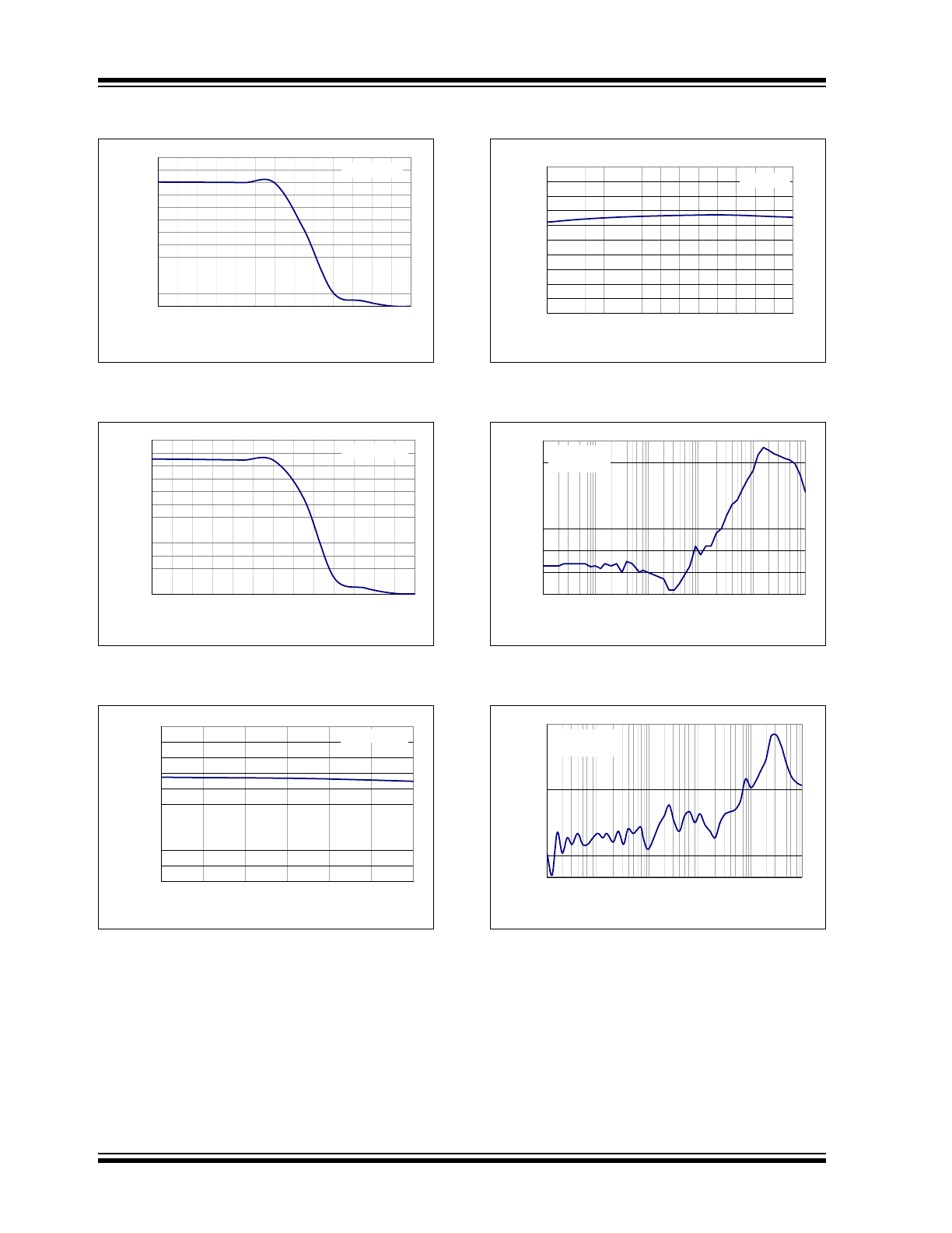
2007-2015 Microchip Technology Inc.
DS20002071C-page 9
MCP73837/8
Note: Unless otherwise indicated, V
DD
= [V
REG
(typical) + 1V], I
OUT
= 30 mA and T
A
= +25°C, Constant-voltage mode.
FIGURE 2-7:
Charge Current (I
OUT
) vs.
Supply Voltage (V
DD
).
FIGURE 2-8:
Charge Current (I
OUT
) vs.
Supply Voltage (V
DD
).
FIGURE 2-9:
Charge Current (I
OUT
) vs.
Ambient Temperature (T
A
).
FIGURE 2-10:
Charge Current (I
OUT
) vs.
Ambient Temperature (T
A
).
FIGURE 2-11:
Charge Current (I
OUT
) vs.
Ambient Temperature (T
A
).
FIGURE 2-12:
Charge Current (I
OUT
) vs.
Junction Temperature (T
J
).
700
750
800
850
900
950
1000
1050
1100
1150
1200
4.5
4.8
5.0
5.3
5.5
5.8
6.0
Supply Voltage (V)
Ch
ar
ge C
u
rr
ent
(
m
A)
R
PROG
= 1 kΩ
Temp = +25°C
90
92
94
96
98
100
102
104
4.5
4.8
5.0
5.3
5.5
5.8
6.0
Supply Voltage (V)
Char
ge Cur
re
n
t (
m
A)
R
PROG
= 10 kΩ
Temp = +25°C
700
750
800
850
900
950
1000
1050
1100
-40 -30 -20 -10 0 10 20 30 40 50 60 70 80
Ambient Temperature (°C)
Ch
ar
g
e Cu
rr
e
n
t (
m
A)
R
PROG
= 1 kΩ
V
DD
= 5.2V
90
92
94
96
98
100
102
104
106
108
110
-40 -30 -20 -10 0 10 20 30 40 50 60 70 80
Ambient Temperature (°C)
Char
ge Cur
rent (
m
A)
R
PROG
= 10 kΩ
V
DD
= 5.2V
45
46
47
48
49
50
51
52
53
54
55
-40 -30 -20 -10 0 10 20 30 40 50 60 70 80
Ambient Temperature (°C)
Char
ge Cur
re
nt
(mA)
R
PROG
= 20 kΩ
V
DD
= 5.2V
0
100
200
300
400
500
600
700
800
900
1000
1100
1200
25
35
45
55
65
75
85
95
105
115
125
135
145
155
Junction Temperature (°C)
C
h
arge C
u
rrent
(
m
A
)
R
PROG
= 1 kΩ
MCP73837/8
DS20002071C-page 10
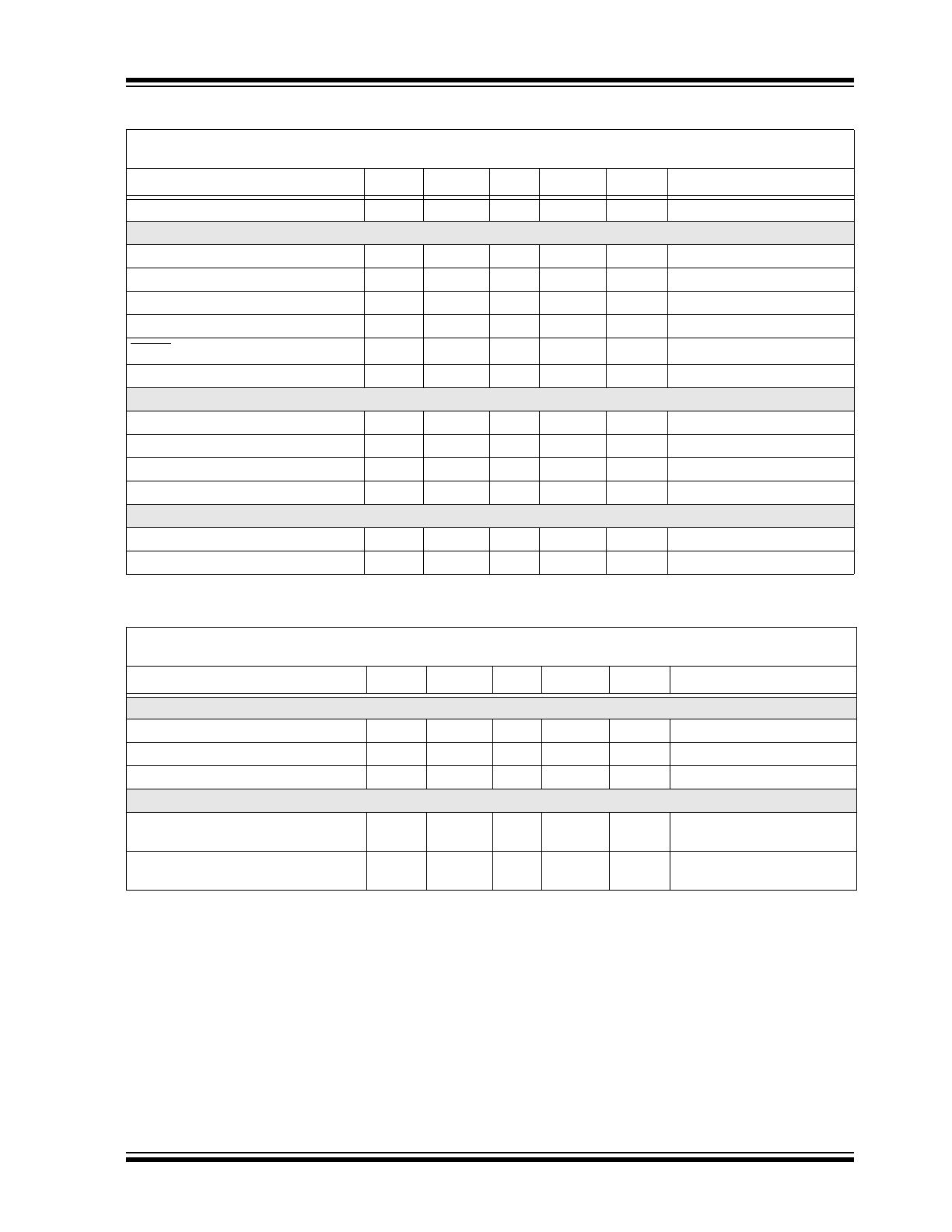
2007-2015 Microchip Technology Inc.
Note: Unless otherwise indicated, V
DD
= [V
REG
(typical) + 1V], I
OUT
= 30 mA and T
A
= +25°C, Constant-voltage mode.
FIGURE 2-13:
Charge Current (I
OUT
) vs.
Junction Temperature (T
J
).
FIGURE 2-14:
Charge Current (I
OUT
) vs.
Junction Temperature (T
J
).
FIGURE 2-15:
Thermistor Current (I
THERM
)
vs. Supply Voltage (V
DD
).
FIGURE 2-16:
Thermistor Current (I
THERM
)
vs. Ambient Temperature (T
A
).
FIGURE 2-17:
Power Supply Ripple
Rejection (PSRR).
FIGURE 2-18:
Power Supply Ripple
Rejection (PSRR).
0
50
100
150
200
250
300
350
400
450
500
550
600
25
35
45
55
65
75
85
95
10
5
11
5
12
5
13
5
14
5
15
5
Junction Temperature (°C)
Ch
a
rg
e
Cu
rr
e
n
t
(m
A
)
R
PROG
= 2 kΩ
0
10
20
30
40
50
60
70
80
90
100
110
120
25
35
45
55
65
75
85
95
105
115
125
135
145
155
Junction Temperature (°C)
Char
ge Cur
re
n
t (
m
A)
R
PROG
= 10 kΩ
47.0
47.5
48.0
48.5
49.0
49.5
50.0
50.5
51.0
51.5
52.0
4.5
4.8
5.0
5.3
5.5
5.8
6.0
Supply Voltage (V)
T
h
er
m
ist
o
r C
u
rr
e
n
t (
m
A
)
Temp = +25°C
47.0
47.5
48.0
48.5
49.0
49.5
50.0
50.5
51.0
51.5
52.0
-4
0
-3
0
-2
0
-1
0
0
10
20
30
40
50
60
70
80
90
Ambient Temperature (°C)
T
h
er
m
is
to
r C
u
rr
en
t (
m
A
)
V
DD
= 5.2V
-70
-60
-50
-40
-30
-20
-10
0
0.01
0.1
1
10
100
1000
Frequency (kHz)
Att
enua
ti
o
n
(d
B
)
I
OUT
= 10 mA
C
OUT
= 4.7 µF
-70
-60
-50
-40
-30
-20
-10
0
0.01
0.1
1
10
100
1000
Frequency (kHz)
Attenu
at
ion (
d
B)
I
OUT
= 100 mA
C
OUT
= 4.7 µF