
2005-2014 Microchip Technology Inc.
DS20001984G-page 1
MCP73831/2
Features:
• Linear Charge Management Controller:
- Integrated Pass Transistor
- Integrated Current Sense
- Reverse Discharge Protection
• High Accuracy Preset Voltage Regulation: + 0.75%
• Four Voltage Regulation Options:
- 4.20V, 4.35V, 4.40V, 4.50V
• Programmable Charge Current: 15 mA to 500 mA
• Selectable Preconditioning:
- 10%, 20%, 40%, or Disable
• Selectable End-of-Charge Control:
- 5%, 7.5%, 10%, or 20%
• Charge Status Output
- Tri-State Output - MCP73831
- Open-Drain Output - MCP73832
• Automatic Power-Down
• Thermal Regulation
• Temperature Range: -40°C to +85°C
• Packaging:
- 8-Lead, 2 mm x 3 mm DFN
- 5-Lead, SOT-23
Applications:
• Lithium-Ion/Lithium-Polymer Battery Chargers
• Personal Data Assistants
• Cellular Telephones
• Digital Cameras
• MP3 Players
• Bluetooth Headsets
• USB Chargers
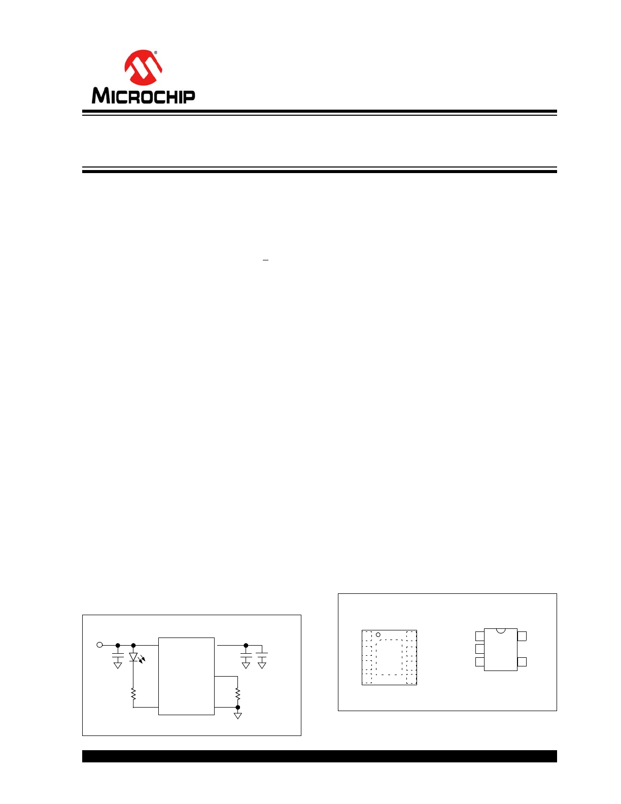
Typical Application
Description:
The MCP73831/2 devices are highly advanced linear
charge management controllers for use in space-
limited, cost-sensitive applications. The MCP73831/2
are available in an 8-Lead, 2 mm x 3 mm DFN package
or a 5-Lead, SOT-23 package. Along with their small
physical size, the low number of external components
required make the MCP73831/2 ideally suited for
portable applications. For applications charging from a
USB port, the MCP73831/2 adhere to all the
specifications governing the USB power bus.
The MCP73831/2 employ a constant-current/constant-
voltage charge algorithm with selectable
preconditioning and charge termination. The constant
voltage regulation is fixed with four available options:
4.20V, 4.35V, 4.40V or 4.50V, to accommodate new,
emerging battery charging requirements. The constant
current value is set with one external resistor. The
MCP73831/2 devices limit the charge current based on
die temperature during high power or high ambient
conditions. This thermal regulation optimizes the
charge cycle time while maintaining device reliability.
Several options are available for the preconditioning
threshold, preconditioning current value, charge
termination value and automatic recharge threshold.
The preconditioning value and charge termination
value are set as a ratio or percentage of the
programmed constant current value. Preconditioning
can be disabled. Refer to
Section 1.0 “Electrical
Characteristics”
for available options and the
Product Identification System
for standard options.
The MCP73831/2 devices are fully specified over the
ambient temperature range of -40°C to +85°C.
Package Types
STAT
V
DD
V
SS
PROG
V
BAT
+
-
Single
Li-Ion
Cell
4
MCP73831
5
3
1
500 mA Li-Ion Battery Charger
2
V
IN
4.7
F
470
2 k
4.7
F
V
BAT
V
SS
V
DD
1
2
3
5
4
PROG
STAT
MCP73831/2
2×3 DFN*
V
BAT
V
DD
V
BAT
NC
V
SS
1
2
3
4
8
7
6
5 STAT
PROG
V
DD
* Includes Exposed Thermal Pad (EP); see
Table 3-1
.
EP
9
MCP73831/2
SOT-23-5
Miniature Single-Cell, Fully Integrated Li-Ion,
Li-Polymer Charge Management Controllers
MCP73831/2
DS20001984G-page 2
2005-2014 Microchip Technology Inc.
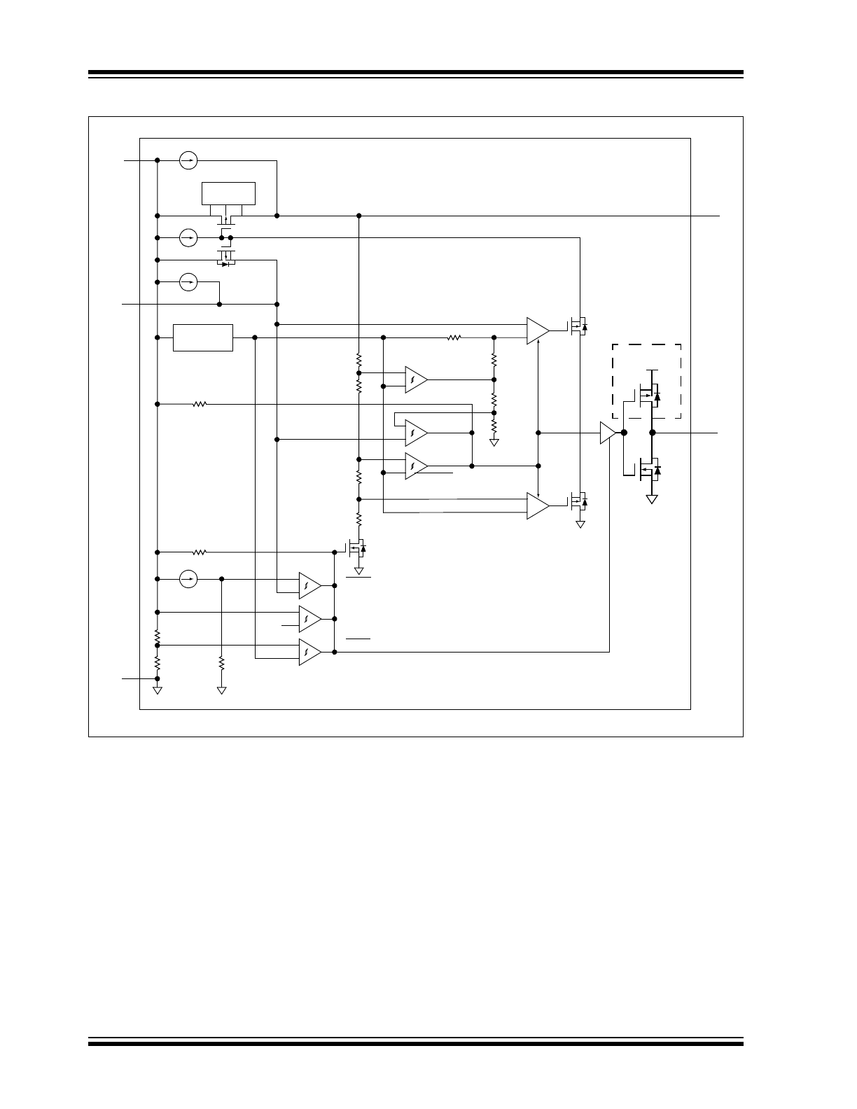
Functional Block Diagram
+
-
REFERENCE
GENERATOR
V
REF
(1.22V)
V
BAT
V
DD
STAT
PROG
V
BAT
G=0.001
V
SS
DIRECTION
CONTROL
477 k
255 k
UVLO
+
-
+
-
SHDN
DIRECTION
CONTROL
0.5 µA
PRECONDITION
6 µA
6 µA
+
-
TERMINATION
+
-
43.6 k
+
-
CA
3.9 k
111 k
190 k
7 k
15 k
182.3 k
111 k
CHARGE
+
-
+
-
VA
89 k
361 k
100 k
0.5 µA
VDD
MCP73831
ONLY
2005-2014 Microchip Technology Inc.
DS20001984G-page 3
MCP73831/2
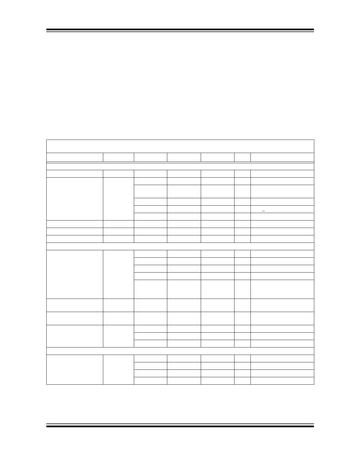
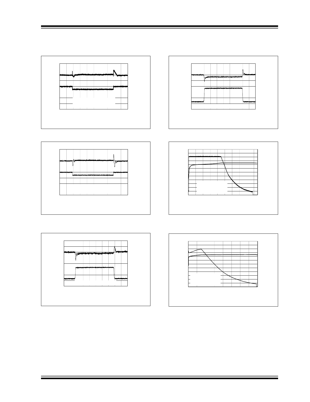
1.0
ELECTRICAL
CHARACTERISTICS
Absolute Maximum Ratings†
V
DD
...................................................................................7.0V
All Inputs and Outputs w.r.t. V
SS
............... -0.3 to (V
DD
+0.3)V
Maximum Junction Temperature, T
J
............ Internally Limited
Storage temperature .....................................-65°C to +150°C
ESD protection on all pins:
Human Body Model (1.5 k
in Series with 100 pF)4 kV
Machine Model (200 pF, No Series Resistance) .............400V
† Notice: Stresses above those listed under “Maximum
Ratings” may cause permanent damage to the device.
This is a stress rating only and functional operation of
the device at those or any other conditions above those
indicated in the operational listings of this specification
is not implied. Exposure to maximum rating conditions
for extended periods may affect device reliability.
DC CHARACTERISTICS
Electrical Specifications: Unless otherwise indicated, all limits apply for V
DD
= [V
REG
(typical) + 0.3V] to 6V, T
A
= -40°C to +85°C.
Typical values are at +25°C, V
DD
= [V
REG
(typical) + 1.0V]
Parameters
Sym.
Min.
Typ.
Max.
Units
Conditions
Supply Input
Supply Voltage
V
DD
3.75
—
6
V
Supply Current
I
SS
—
510
1500
µA
Charging
—
53
200
µA
Charge Complete,
No Battery
—
25
50
µA
PROG Floating
—
1
5
µA
V
DD
< (V
BAT
- 50 mV)
—
0.1
2
µA
V
DD
< V
STOP
UVLO Start Threshold
V
START
3.3
3.45
3.6
V
V
DD
Low-to-High
UVLO Stop Threshold
V
STOP
3.2
3.38
3.5
V
V
DD
High-to-Low
UVLO Hysteresis
V
HYS
—
70
—
mV
Voltage Regulation (Constant-Voltage Mode)
Regulated Output Voltage
V
REG
4.168
4.20
4.232
V
MCP7383X-2
4.317
4.35
4.383
V
MCP7383X-3
4.367
4.40
4.433
V
MCP7383X-4
4.466
4.50
4.534
V
MCP7383X-5
V
DD
= [V
REG
(typical)+1V]
I
OUT
= 10 mA
T
A
= -5°C to +55°C
Line Regulation
V
BAT
/
V
BAT
)/
V
DD
|
—
0.09
0.30
%/V
V
DD
= [V
REG
(typical)+1V] to
6V, I
OUT
= 10 mA
Load Regulation
V
BAT
/V
BAT
|
—
0.05
0.30
%
I
OUT
= 10 mA to 50 mA
V
DD
= [V
REG
(typical)+1V]
Supply Ripple Attenuation
PSRR
—
52
—-
dB
I
OUT
=10 mA, 10Hz to 1 kHz
—
47
—
dB
I
OUT
=10 mA, 10Hz to 10 kHz
—
22
—
dB
I
OUT
=10 mA, 10Hz to 1 MHz
Current Regulation (Fast Charge Constant-Current Mode)
Fast Charge Current
Regulation
I
REG
90
100
110
mA
PROG = 10 k
450
505
550
mA
PROG = 2.0 k
Note 1
12.5
14.5
16.5
mA
PROG = 67 k
T
A
= -5°C to +55°C
Note 1:
Not production tested. Ensured by design.
MCP73831/2
DS20001984G-page 4
2005-2014 Microchip Technology Inc.
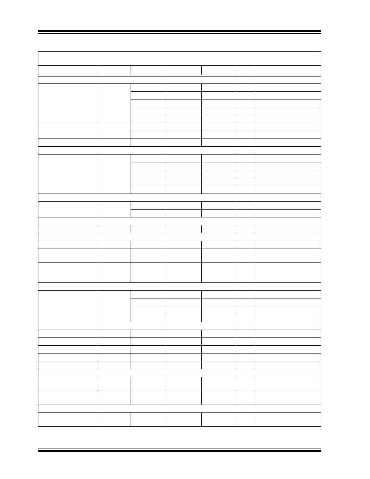
Preconditioning Current Regulation (Trickle Charge Constant-Current Mode)
Precondition Current
Ratio
I
PREG
/ I
REG
7.5
10
12.5
%
PROG = 2.0 k
to 10 k
15
20
25
%
PROG = 2.0 k
to 10 k
30
40
50
%
PROG = 2.0 k
to 10 k
—
100
—
%
No Preconditioning
T
A
= -5°C to +55°C
Precondition Voltage
Threshold Ratio
V
PTH
/ V
REG
64
66.5
69
%
V
BAT
Low-to-High
69
71.5
74
%
V
BAT
Low-to-High
Precondition Hysteresis
V
PHYS
—
110
—
mV
V
BAT
High-to-Low
Charge Termination
Charge Termination
Current Ratio
I
TERM
/ I
REG
3.75
5
6.25
%
PROG = 2.0 k
to 10 k
5.6
7.5
9.4
%
PROG = 2.0 k
to 10 k
8.5
10
11.5
%
PROG = 2.0 k
to 10 k
15
20
25
%
PROG = 2.0 k
to 10 k
T
A
= -5°C to +55°C
Automatic Recharge
Recharge Voltage
Threshold Ratio
V
RTH
/ V
REG
91.5
94.0
96.5
%
V
BAT
High-to-Low
94
96.5
99
%
V
BAT
High-to-Low
Pass Transistor ON-Resistance
ON-Resistance
R
DSON
—
350
—
m
V
DD
= 3.75V, T
J
= 105°C
Battery Detection
Battery Detection Current
I
BAT_DET
—
6
—
µA
V
BAT
Source Current
No-Battery-Present
Threshold
V
NO_BAT
—
V
REG
+
100 mV
—
V
V
BAT
Voltage
≥
V
NO_BAT
for
No Battery condition
No-Battery-Present
Impedance
Z
NO_BAT
2
—
—
M
V
BAT
Impedance
≥
Z
NO_BAT
for No Battery condition,
Note 1
Battery Discharge Current
Output Reverse Leakage
Current
I
DISCHARGE
—
0.15
2
µA
PROG Floating
—
0.25
2
µA
V
DD
Floating
—
0.15
2
µA
V
DD
< V
STOP
—
-5.5
-15
µA
Charge Complete
Status Indicator – STAT
Sink Current
I
SINK
—
—
25
mA
Low Output Voltage
V
OL
—
0.4
1
V
I
SINK
= 4 mA
Source Current
I
SOURCE
—
—
35
mA
High Output Voltage
V
OH
—
V
DD
-0.4
V
DD
- 1
V
I
SOURCE
= 4 mA (MCP73831)
Input Leakage Current
I
LK
—
0.03
1
µA
High-Impedance
PROG Input
Charge Impedance
Range
R
PROG
2
—
67
k
Minimum Shutdown
Impedance
R
PROG
70
—
200
k
Automatic Power Down
Automatic Power Down
Entry Threshold
V
PDENTER
V
DD
<(V
BAT
+20 mV)
V
DD
<(V
BAT
+50 mV)
—
3.5V
V
BAT
V
REG
V
DD
Falling
DC CHARACTERISTICS (CONTINUED)
Electrical Specifications: Unless otherwise indicated, all limits apply for V
DD
= [V
REG
(typical) + 0.3V] to 6V, T
A
= -40°C to +85°C.
Typical values are at +25°C, V
DD
= [V
REG
(typical) + 1.0V]
Parameters
Sym.
Min.
Typ.
Max.
Units
Conditions
Note 1:
Not production tested. Ensured by design.
2005-2014 Microchip Technology Inc.
DS20001984G-page 5
MCP73831/2
TEMPERATURE SPECIFICATIONS
Automatic Power Down
Exit Threshold
V
PDEXIT
—
V
DD
<(V
BAT
+150 mV)
V
DD
<(V
BAT
+200 mV)
3.5V
V
BAT
V
REG
V
DD
Rising
Thermal Shutdown
Die Temperature
T
SD
—
150
—
C
Die Temperature
Hysteresis
T
SDHYS
—
10
—
C
DC CHARACTERISTICS (CONTINUED)
Electrical Specifications: Unless otherwise indicated, all limits apply for V
DD
= [V
REG
(typical) + 0.3V] to 6V, T
A
= -40°C to +85°C.
Typical values are at +25°C, V
DD
= [V
REG
(typical) + 1.0V]
Parameters
Sym.
Min.
Typ.
Max.
Units
Conditions
Note 1:
Not production tested. Ensured by design.
AC CHARACTERISTICS
Electrical Specifications: Unless otherwise indicated, all limits apply for V
DD
= [V
REG
(typical) + 0.3V] to 12V,
T
A
= -40°C to +85°C. Typical values are at +25°C, V
DD
= [V
REG
(typical) + 1.0V]
Parameters
Sym.
Min.
Typ.
Max.
Units
Conditions
UVLO Start Delay
t
START
—
—
5
ms
V
DD
Low-to-High
Constant-Current Regulation
Transition Time Out of
Preconditioning
t
DELAY
—
—
1
ms
V
BAT
< V
PTH
to V
BAT
> V
PTH
Current Rise Time Out of
Preconditioning
t
RISE
—
—
1
ms
I
OUT
Rising to 90% of I
REG
Termination Comparator
Filter
t
TERM
0.4
1.3
3.2
ms
Average I
OUT
Falling
Charge Comparator Filter
t
CHARGE
0.4
1.3
3.2
ms
Average V
BAT
Status Indicator
Status Output turn-off
t
OFF
—
—
200
µ
s
I
SINK
= 1 mA to 0 mA
Status Output turn-on
t
ON
—
—
200
µ
s
I
SINK
= 0 mA to 1 mA
Electrical Specifications: Unless otherwise indicated, all limits apply for V
DD
= [V
REG
(typical) + 0.3V] to 12V.
Typical values are at +25°C, V
DD
= [V
REG
(typical) + 1.0V]
Parameters
Sym.
Min.
Typ.
Max.
Units
Conditions
Temperature Ranges
Specified Temperature Range
T
A
-40
—
+85
°C
Operating Temperature Range
T
J
-40
—
+125
°C
Storage Temperature Range
T
A
-65
—
+150
°C
Thermal Package Resistances
5-Lead, SOT-23
JA
—
230
—
°C/W
4-Layer JC51-7 Standard
Board, Natural Convection
(
Note 2
)
8-Lead, 2 mm x 3 mm, DFN
JA
—
76
—
°C/W
4-Layer JC51-7 Standard
Board, Natural Convection
(
Note 1
)
Note 1:
This represents the minimum copper condition on the PCB (Printed Circuit Board).
2:
With large copper area on the PCB, the SOT-23-5 thermal resistance (
JA
) can reach a typical value of
130°C/W or better.

MCP73831/2
DS20001984G-page 6
2005-2014 Microchip Technology Inc.
NOTES:
2005-2014 Microchip Technology Inc.
DS20001984G-page 7
MCP73831/2
2.0
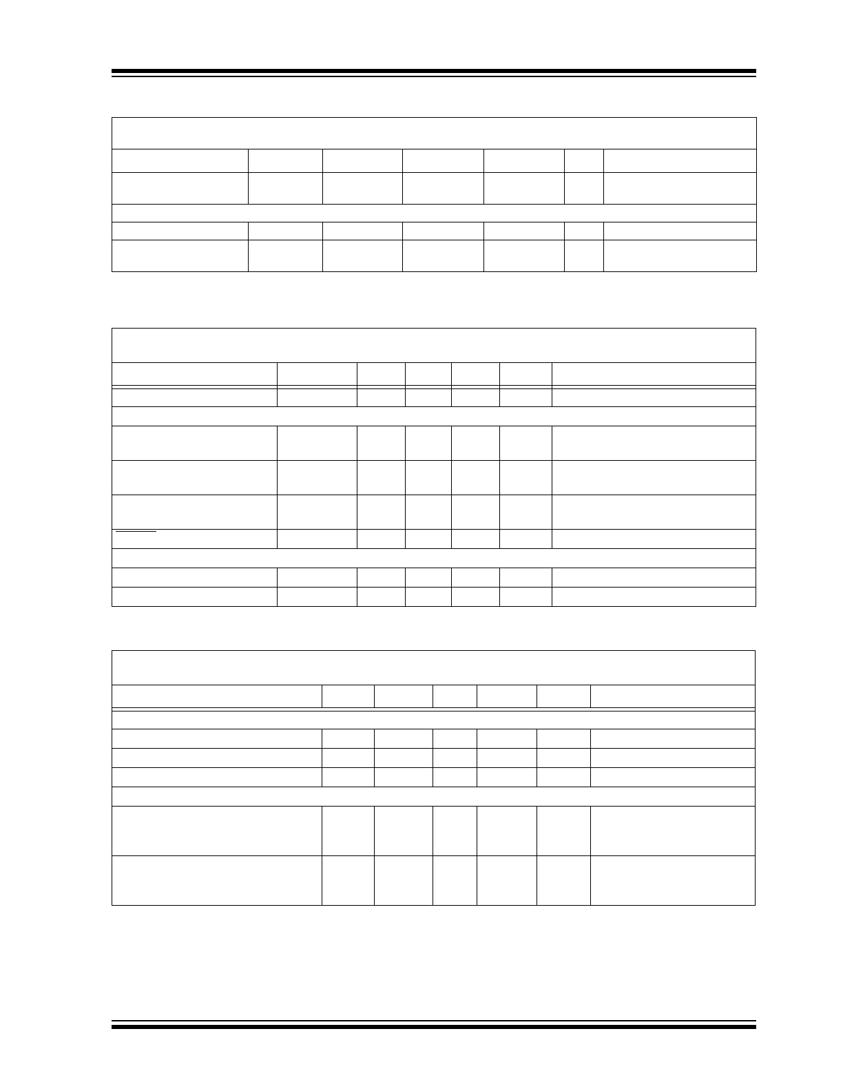
TYPICAL PERFORMANCE CURVES
Note: Unless otherwise indicated, V
DD
= [V
REG
(typical) + 1V], I
OUT
= 10 mA and T
A
= +25°C, Constant-Voltage mode.
FIGURE 2-1:
Battery Regulation Voltage
(V
BAT
) vs. Supply Voltage (V
DD
).
FIGURE 2-2:
Battery Regulation Voltage
(V
BAT
) vs. Ambient Temperature (T
A
).
FIGURE 2-3:
Output Leakage Current
(I
DISCHARGE
) vs. Battery Regulation Voltage
(V
BAT
).
FIGURE 2-4:
Charge Current (I
OUT
) vs.
Programming Resistor (R
PROG
).
FIGURE 2-5:
Charge Current (I
OUT
) vs.
Supply Voltage (V
DD
).
FIGURE 2-6:
Charge Current (I
OUT
) vs.
Supply Voltage (V
DD
).
Note:
The graphs and tables provided following this note are a statistical summary based on a limited number of
samples and are provided for informational purposes only. The performance characteristics listed herein
are not tested or guaranteed. In some graphs or tables, the data presented may be outside the specified
operating range (e.g., outside specified power supply range) and therefore outside the warranted range.
4.170
4.175
4.180
4.185
4.190
4.195
4.200
4.205
4.210
4.50
4.75
5.00
5.25
5.50
5.75
6.00
Supply Voltage (V)
B
at
te
ry R
e
gul
atio
n
V
o
lt
ag
e
(V
)
MCP73831-2
I
OUT
= 10 mA
I
OUT
= 100 mA
I
OUT
= 450 mA
4.170
4.175
4.180
4.185
4.190
4.195
4.200
4.205
4.210
-40
-30
-20
-10
0
10
20
30
40
50
60
70
80
Ambient Temperature (°C)
B
a
tt
er
y
R
egul
at
io
n V
o
lt
age
(
V
)
MCP73831-2
I
OUT
= 10 mA
I
OUT
= 100 mA
I
OUT
= 450 mA
0.00
0.05
0.10
0.15
0.20
0.25
0.30
0.35
0.40
3.00
3.20
3.40
3.60
3.80
4.00
4.20
Battery Regulation Voltage (V)
O
u
tp
ut Le
ak
age
C
u
rr
e
nt
(µA
)
+85°C
-40°C
+25°C
0
50
100
150
200
250
300
350
400
450
500
2
7 12 17 22 27 32 37 42 47 52 57 62 67
Programming Resistor (kΩ)
Ch
ar
g
e
Cu
rr
e
n
t (
m
A)
96
97
98
99
100
101
102
103
104
4.50
4.75
5.00
5.25
5.50
5.75
6.00
Supply Voltage (V)
Ch
a
rg
e Cu
rr
e
n
t
(m
A
)
R
PROG
= 10 kΩ
500
502
504
506
508
510
512
514
516
4.50
4.75
5.00
5.25
5.50
5.75
6.00
Supply Voltage (V)
Ch
ar
g
e Cu
rre
n
t (
m
A)
R
PROG
= 2 kΩ
MCP73831/2
DS20001984G-page 8
2005-2014 Microchip Technology Inc.
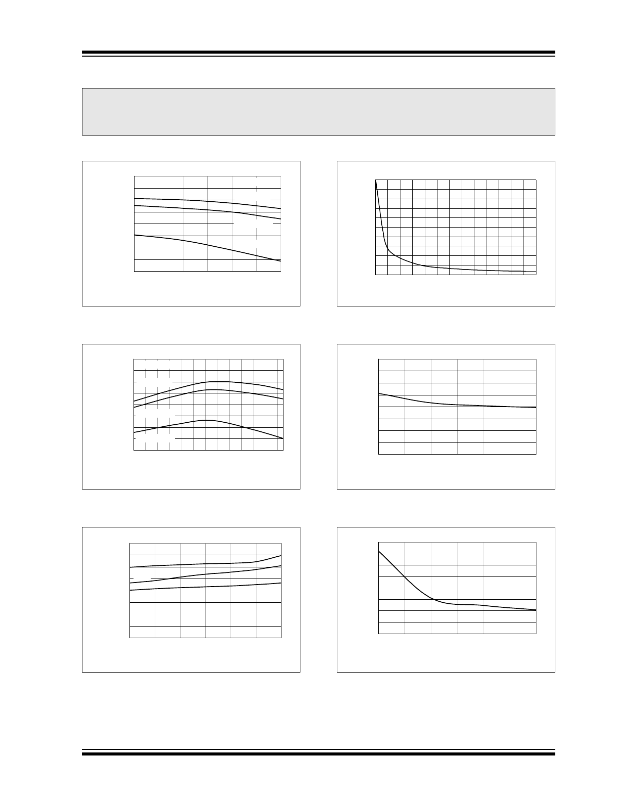
TYPICAL PERFORMANCE CURVES
(CONTINUED)
Note: Unless otherwise indicated, V
DD
= [V
REG
(typical) + 1V], I
OUT
= 10 mA and T
A
= +25°C, Constant-Voltage mode.
FIGURE 2-7:
Charge Current (I
OUT
) vs.
Ambient Temperature (T
A
).
FIGURE 2-8:
Charge Current (I
OUT
) vs.
Ambient Temperature (T
A
).
FIGURE 2-9:
Charge Current (I
OUT
) vs.
Junction Temperature (T
J
).
FIGURE 2-10:
Charge Current (I
OUT
) vs.
Junction Temperature (T
J
).
FIGURE 2-11:
Power Supply Ripple
Rejection (PSRR).
FIGURE 2-12:
Power Supply Ripple
Rejection (PSRR).
96
97
98
99
100
101
102
103
104
-4
0
-3
0
-2
0
-1
0
0
10
20
30
40
50
60
70
80
Ambient Temperature (°C)
C
h
arg
e C
u
rr
e
n
t
(m
A
)
R
PROG
= 10 kΩ
500
502
504
506
508
510
512
514
516
-40
-30
-20
-10
0
10
20
30
40
50
60
70
80
Ambient Temperature (°C)
C
h
ar
ge C
u
rr
ent
(m
A
)
R
PROG
= 2 kΩ
0
15
30
45
60
75
90
105
120
25
35
45
55
65
75
85
95
105
115
125
135
145
155
Junction Temperature (°C)
Ch
a
rg
e Cu
rr
en
t (
m
A)
R
PROG
= 10 kΩ
0
75
150
225
300
375
450
525
25
35
45
55
65
75
85
95
105
115
125
135
145
155
Junction Temperature (°C)
Ch
a
rg
e
Cu
rr
en
t (
m
A)
R
PROG
= 2 kΩ
-60
-50
-40
-30
-20
-10
0
0.01
0.1
1
10
100
1000
Frequency (kHz)
At
te
n
u
a
ti
o
n
(
d
B)
V
AC
= 100 mVp-p
I
OUT
= 10 mA
C
OUT
= 4.7 µF, X7R Ceramic
-60
-50
-40
-30
-20
-10
0
0.01
0.1
1
10
100
1000
Frequency (kHz)
A
tt
enu
ati
o
n (
d
B
)
V
AC
= 100 mVp-p
I
OUT
= 100 mA
C
OUT
= 4.7 µF, X7R Ceramic
2005-2014 Microchip Technology Inc.
DS20001984G-page 9
MCP73831/2
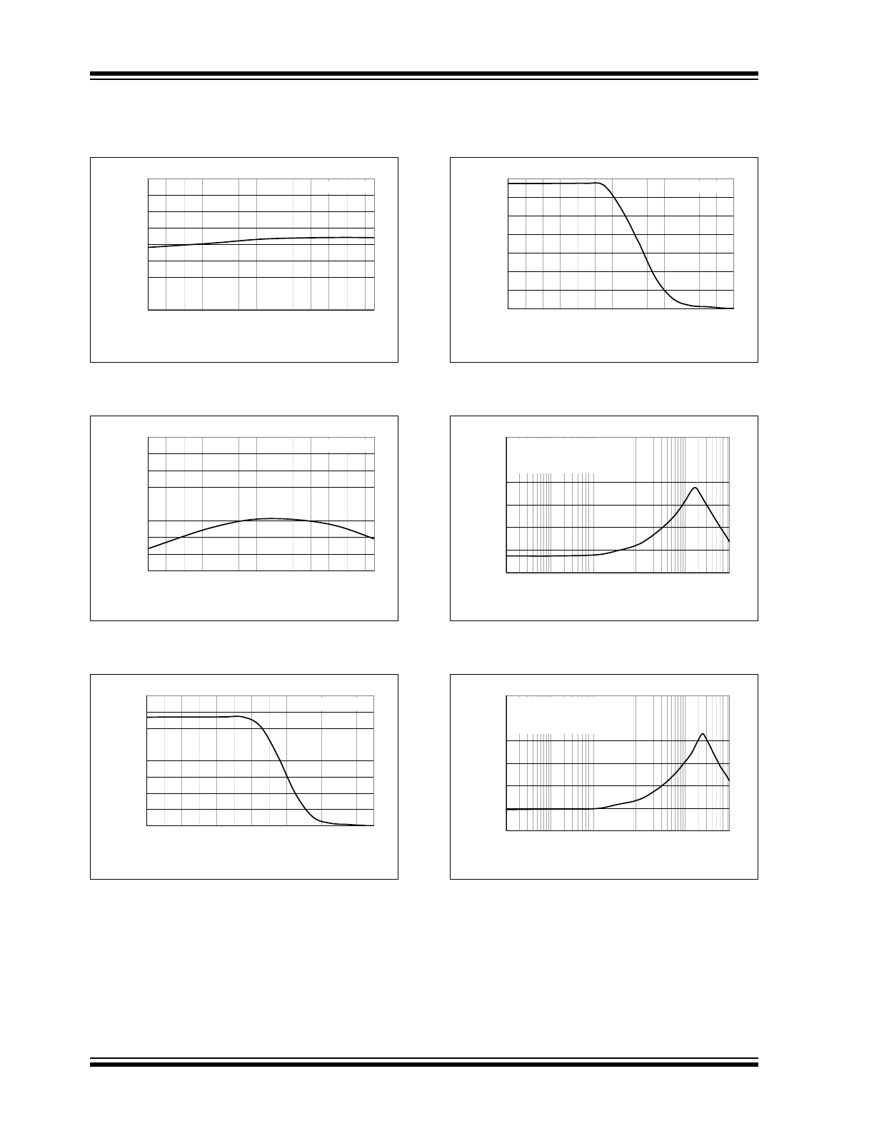
TYPICAL PERFORMANCE CURVES
(CONTINUED)
Note: Unless otherwise indicated, V
DD
= [V
REG
(typical) + 1V], I
OUT
= 10 mA and T
A
= +25°C, Constant-Voltage mode.
FIGURE 2-13:
Line Transient Response.
FIGURE 2-14:
Line Transient Response.
FIGURE 2-15:
Load Transient Response.
FIGURE 2-16:
Load Transient Response.
FIGURE 2-17:
Complete Charge Cycle
(180 mAh Li-Ion Battery).
FIGURE 2-18:
Complete Charge Cycle
(1000 mAh Li-Ion Battery).
-2
0
2
4
6
8
10
12
14
0
20
40
60
80
100
120
140
160
180
200
Time (µs)
S
our
ce V
o
lt
age
(V
)
-0.30
-0.25
-0.20
-0.15
-0.10
-0.05
0.00
0.05
0.10
O
u
tp
ut R
ippl
e
(V
)
I
OUT
= 10 mA
C
OUT
= 4.7 µF, X7R Ceramic
-2
0
2
4
6
8
10
12
14
0
20
40
60
80
100
120
140
160
180
200
Time (µs)
S
o
ur
ce V
o
lt
age
(V
)
-0.30
-0.25
-0.20
-0.15
-0.10
-0.05
0.00
0.05
0.10
O
u
tput
R
ip
p
le
(V
)
I
OUT
= 100 mA
C
OUT
= 4.7 µF, X7R Ceramic
-0.05
0.00
0.05
0.10
0.15
0.20
0.25
0.30
0.35
0
20
40
60
80
100
120
140
160
180
200
Time (µs)
O
u
tp
ut
C
u
rr
en
t (
A
)
-0.12
-0.10
-0.08
-0.06
-0.04
-0.02
0.00
0.02
0.04
O
u
tp
ut
R
ipp
le
(
V
)
C
OUT
= 4.7 µF, X7R Ceramic
-0.20
0.00
0.20
0.40
0.60
0.80
1.00
1.20
1.40
0
20
40
60
80
100
120
140
160
180
200
Time (µs)
O
u
tput
C
u
rr
en
t (
A
)
-0.30
-0.25
-0.20
-0.15
-0.10
-0.05
0.00
0.05
0.10
O
u
tp
ut R
ippl
e
(V
)
C
OUT
= 4.7 µF, X7R Ceramic
0.0
1.0
2.0
3.0
4.0
5.0
6.0
0
20
40
60
80
100
120
140
160
180
Time (minutes)
B
att
er
y V
o
lt
age
(V
)
0
20
40
60
80
100
120
C
h
ar
ge
C
u
rr
en
t
(m
A
)
MCP73831-2AC/IOT
V
DD
= 5.2V
R
PROG
= 10 kΩ
0.0
1.0
2.0
3.0
4.0
5.0
6.0
0
30
60
90
120
150
180
210
240
Time (minutes)
B
att
er
y V
o
lta
g
e (
V
)
0
100
200
300
400
500
600
Ch
ar
g
e Cu
rr
en
t (
m
A)
MCP73831-2AC/IOT
V
DD
= 5.2V
R
PROG
= 2 kΩ

MCP73831/2
DS20001984G-page 10
2005-2014 Microchip Technology Inc.
NOTES: