
2011-2014 Microchip Technology Inc.
DS20005049D-page 1
MCP73830/L
Features:
• Complete Linear Charge Management Controller:
- Integrated Pass Transistor
- Integrated Current Sense
- Integrated Reverse Discharge Protection
• Constant Current/Constant Voltage Operation
• High Accuracy Preset Voltage Regulation:
– 4.20V + 0.75%
• Programmable Charge Current:
– MCP73830L: 20 mA – 200 mA
– MCP73830: 100 mA – 1000 mA
• Soft-Start to avoid In-Rush Current
• Preconditioning:
– 10% and no preconditioning
• Fixed Elapsed Timer: 4 Hours
• Fixed Preconditioning Timer: 1 Hour
• Automatic Recharge: No Auto-Recharge is also
available with Selected Options
• Automatic End-of-Charge Control Termination:
– 7.5% and 10%
• Automatic Power-Down when Input Power
Removed
• Undervoltage Lockout (UVLO)
• Chip/Charge Enable Pin (CE)
• Packaging:
– TDFN-6 (2x2 mm)
• Temperature Range: -40°C to +85°C
Applications:
• Bluetooth Headsets
• Portable Media Players
• Rechargeable 3D Glasses
• Toy and Gaming Controllers
Description:
The MCP73830/L are highly integrated, Li-Ion battery
charge management controllers for use in space-
limited applications. The MCP73830/L devices provide
specific charge algorithms for single-cell Li-Ion/Li-
Polymer batteries to achieve optimal capacity and
safety in the shortest charging time possible. Along
with its small physical size, the low number of external
components makes the MCP73830/L ideally suitable
for portable applications.
The MCP73830L employs a constant current/constant
voltage charge algorithm. The minimum 20 mA
regulated constant, fast-charge current enables the
design in small Li-Ion batteries and low-supply current
applications. The fast-charge, constant current value is
set with one external resistor from 20 mA to 200 mA.
The MCP73830/L allows up to 1000 mA charge current
for applications that require faster constant current.
The MCP73830/L provides a thermal foldback function
that limits the charge current based on die temperature
during high-power or high-ambient conditions. This
thermal regulation optimizes the charge cycle time
while maintaining device reliability.
The MCP73830/L is fully specified over the ambient
temperature range of -40°C to +85°C. The
MCP73830/L is available in a 6 lead, TDFN package.
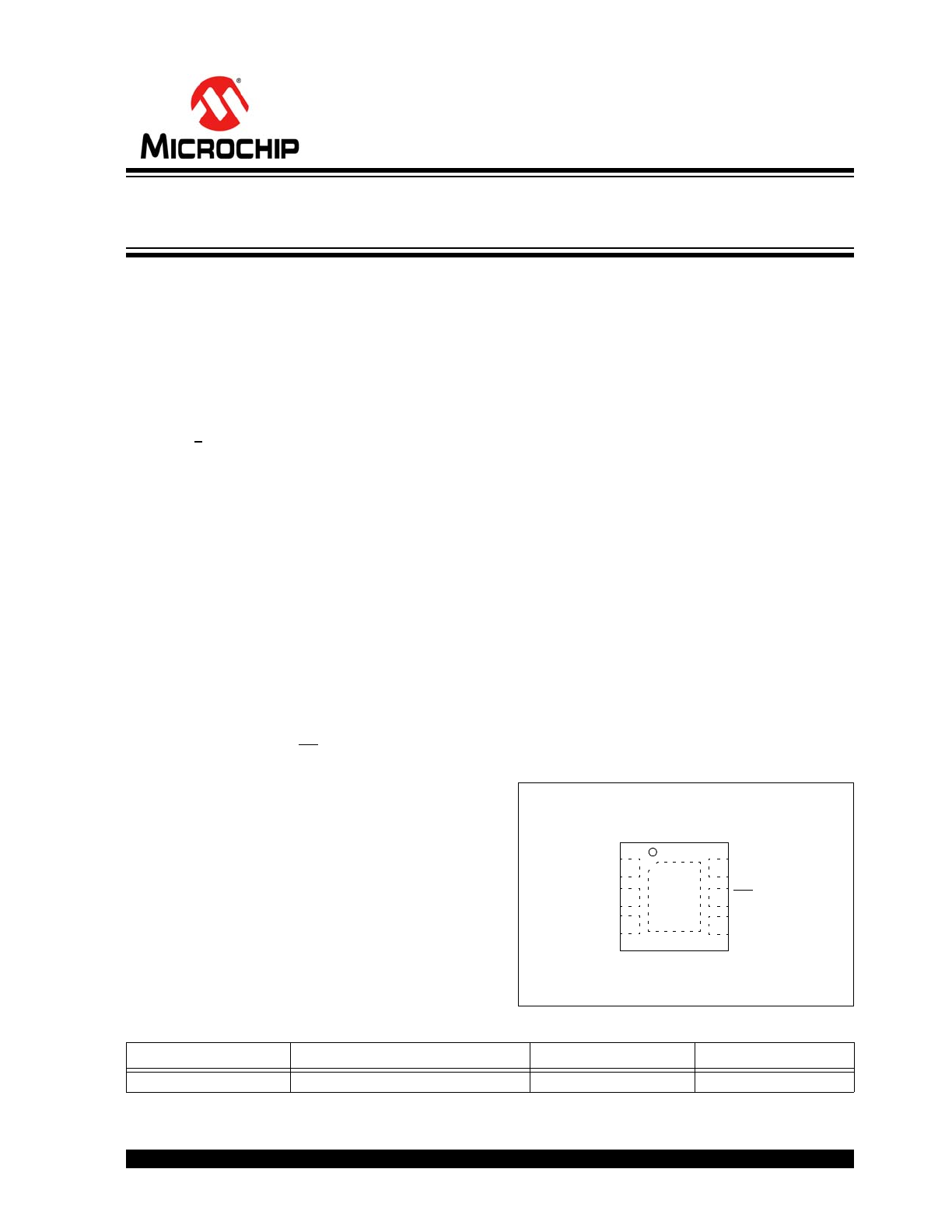
Package Types (Top View)
MCP73830/L
2x2 TDFN *
* Includes Exposed Thermal Pad (EP); see
Table 3-1
.
V
BAT
STAT
CE
V
DD
1
2
3
6
5
4
PROG
V
SS
EP
7
TABLE 1:
AVAILABLE FACTORY PRESET OPTIONS
Charge Voltage
Preconditioning Charge Current
End-of-Charge Control
Auto-Recharge
4.2V
10%/Disabled
7.5%/ 10%
Yes/No
Single-Cell Li-Ion/Li-Polymer Battery Charge Management
Controllers in 2x2 TDFN
MCP73830/L
DS20005049D-page 2
2011-2014 Microchip Technology Inc.
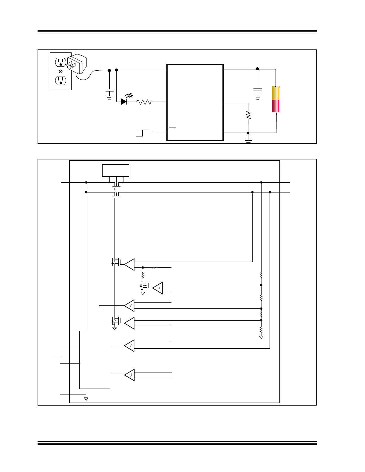
Typical Application
Functional Block Diagram
STAT
V
DD
V
BAT
3
4
PROG
1
2
6
Regulated
wall cube
4.7 µF
2 k
+
-
1-Cell
Li-Ion
Battery
V
SS
5
4.7 µF
1 k
CE
Hi
Lo
MCP73830/L
STAT
PROG
V
BAT
V
SS
Direction
Control
TERM
+
-
UVLO,
Reference,
Charge
Control,
Timer and
Status Logic
G=0.001
V
DD
+
-
CA
V
REF
PRECONDITION
+
-
V
REF
+
-
VA
V
REF
V
REF
CE
CHRG
+
-
V
REF
UVLO
+
-
V
REF
V
DD
2011-2014 Microchip Technology Inc.
DS20005049D-page 3
MCP73830/L
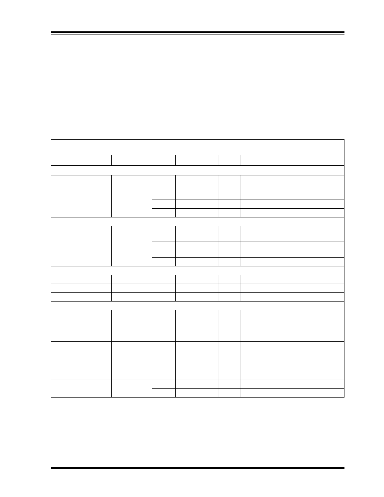
1.0
ELECTRICAL
CHARACTERISTICS
Absolute Maximum Ratings†
V
DD
...................................................................................7.0V
All Inputs and Outputs w.r.t. V
SS
............... -0.3 to (V
DD
+0.3)V
Maximum Junction Temperature, T
J
............ Internally Limited
Storage temperature .....................................-65°C to +150°C
ESD protection on all pins
Human Body Model (1.5 kW in Series with 100 pF)
2 kV
Machine Model (200 pF, No Series Resistance) .............300V
† Notice: Stresses above those listed under “Maximum
Ratings” may cause permanent damage to the device.
This is a stress rating only and functional operation of
the device at those or any other conditions above those
indicated in the operational listings of this specification
is not implied. Exposure to maximum rating conditions
for extended periods may affect device reliability.
DC CHARACTERISTICS
Electrical Specifications: Unless otherwise indicated, all limits apply for V
DD
= [V
REG
(Typical) + 0.3V] to 6V,
T
A
= -40°C to +85°C. Typical values are at +25°C, V
DD
= [V
REG
(Typical) + 1.0V]
Parameters
Sym.
Min.
Typ.
Max.
Units
Conditions
Supply Input
Input Voltage Range
V
DD
3.75
—
6
V
Supply Current
I
SS
—
0.6
2
µA
Shutdown;
V
DD
V
STOP
- 300 mV
—
500
900
µA
Charging
—
25
50
µA
Standby; CE = V
DD
Battery Discharge Current
Output Reverse
Leakage Current
I
DISCHARGE
10
15
µA
Charge Complete;
V
DD
is Present
—
0.5
—
µA
Shutdown
(V
DD
V
BAT
, or V
DD
< V
STOP
)
—
0.5
—
µA
Standby; CE = V
DD
Undervoltage Lockout
UVLO Start Threshold
V
START
3.45
3.6
3.75
V
V
DD
Low-to-High
UVLO Stop Threshold
V
STOP
3.15
3.3
3.45
V
V
DD
High-to-Low
UVLO Hysteresis
V
HYS
—
300
—
mV
Voltage Regulation (Constant Voltage Mode)
Regulated Output
Voltage Options
V
REG
—
4.20
—
V
V
DD
= [V
REG
(Typical)+1V]
I
OUT
= 30 mA
Output Voltage
Tolerance
V
RTOL
-0.75
—
0.75
%
T
A
= -5°C to +55°C
Line Regulation
V
BAT
/V
BAT
)/
V
DD
|
—
0.2
0.3
%/V
V
DD
= [V
REG
(Typical)+1V] to
12V
I
OUT
= 30 mA
Load Regulation
V
BAT
/V
BAT
|
—
0.2
0.3
%
I
OUT
= 30 mA - 150 mA
V
DD
= [V
REG
(Typical)+1V]
Supply Ripple
Attenuation
PSRR
52
—
dB
I
OUT
= 30 mA, 10 Hz to 1 kHz
47
—
dB
I
OUT
= 30 mA, 10 Hz to 10 kHz
Note 1:
Not production tested. Ensured by design.
MCP73830/L
DS20005049D-page 4
2011-2014 Microchip Technology Inc.
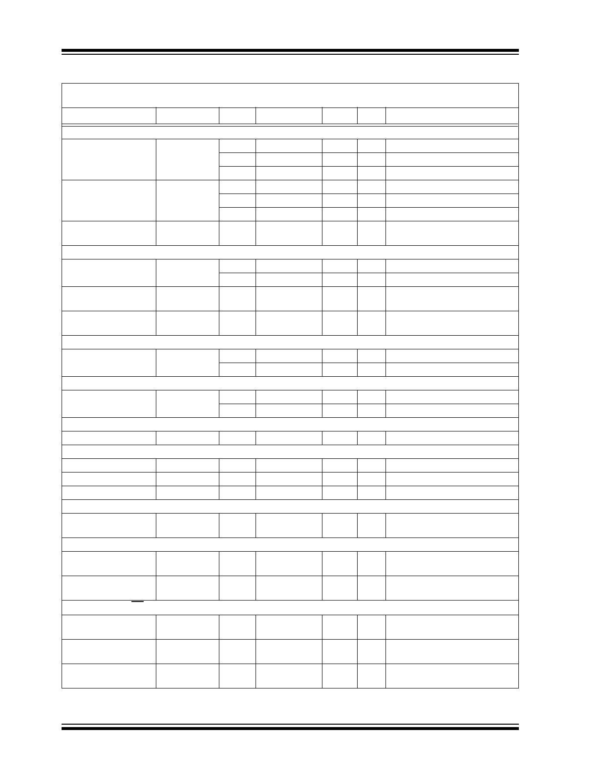
Current Regulation (Fast Charge, Constant-Current Mode)
Fast Charge Current
Regulation
MCP73830L
I
REG
20
—
200
mA
—
20
—
mA
PROG = 10 k
—
200
—
mA
PROG = 1 k
Fast Charge Current
Regulation
MCP73830
I
REG
100
—
1000
mA
—
100
—
mA
PROG = 10 k
—
1000
—
mA
PROG = 1 k
Charge Current
Tolerance
I
RTOL
—
10
—
%
V
DD
= 4.5V, T
A
= -5°C to +55°C
Preconditioning Current Regulation (Trickle Charge Constant Current Mode)
Precondition Current
Ratio
I
PREG
/I
REG
—
10
—
%
PROG = 1 k
to 10 k
—
100
—
%
No Preconditioning
Precondition Voltage
Threshold Ratio
V
PTH
/V
REG
70
72
75
%
V
BAT
Low-to-High
T
A
= -5°C to +55°C
Precondition
Hysteresis
V
PHYS
—
100
—
mV
Charge Termination
Charge Termination
Current Ratio
I
TERM
/I
REG
5.6
7.5
9.4
%
PROG = 1 k
to 10 k
8
10
12
%
V
DD
= 4.5V, T
A
=-5°C to +55°C
Automatic Recharge
Recharge Voltage
Threshold Ratio
V
RTH
/V
REG
94.5
96.5
98.5
%
V
BAT
High-to-Low
—
0
—
%
No Automatic Recharge
Pass Transistor ON-Resistance
ON-Resistance
R
DSON
—
500
—
m
V
DD
= 4.5V, T
J
= 105°C (
Note 1
)
Status Indicator – STAT
Sink Current
I
SINK
—
16
30
mA
Low Output Voltage
V
OL
—
0.4
1
V
I
SINK
= 4 mA
Input Leakage Current
I
LK
—
0.01
1
µA
High Impedance, V
DD
on Pin
PROG Input
Charge Impedance
Range
R
PROG
1
—
10
k
Automatic Power Down
Automatic Power
Down Entry Threshold
V
PDENTRY
—
V
BAT
+ 50 mV
—
V
V
DD
Falling
Automatic Power
Down Exit Threshold
V
PDEXIT
—
V
BAT
+ 150 mV
—
V
V
DD
Rising
Charge Enable (CE)
Input High Voltage
Level
T
SD
1.5
—
—
V
Input Low Voltage
Level
V
IL
—
—
0.8
V
Input Leakage Current
I
LK
—
5
8
µA
V
DD
= 5V
T
A
= -5°C to +55°C
DC CHARACTERISTICS (CONTINUED)
Electrical Specifications: Unless otherwise indicated, all limits apply for V
DD
= [V
REG
(Typical) + 0.3V] to 6V,
T
A
= -40°C to +85°C. Typical values are at +25°C, V
DD
= [V
REG
(Typical) + 1.0V]
Parameters
Sym.
Min.
Typ.
Max.
Units
Conditions
Note 1:
Not production tested. Ensured by design.
2011-2014 Microchip Technology Inc.
DS20005049D-page 5
MCP73830/L
Thermal Shutdown
Die Temperature
T
SD
—
150
—
C
Die Temperature
Hysteresis
T
SDHYS
—
10
—
C
AC CHARACTERISTICS
Electrical Specifications: Unless otherwise specified, all limits apply for V
DD
= [V
REG
(Typical)+0.3V] to 6V,
T
A
= -40°C to +85°C. Typical values are at +25°C, V
DD
= [V
REG
(Typical)+1.0V]
Parameters
Sym.
Min.
Typ.
Max.
Units
Conditions
Elapsed Timer
Elapsed Timer Period
t
ELAPSED
3.5
4.0
4.5
Hours
Preconditioning Timer
Preconditioning Timer Period
t
PRECHG
0.8
1
1.2
Hours
Status Indicator
Status Output Turn-Off
t
OFF
—
—
500
µs
I
SINK
= 1 mA to 0 mA (
Note 1
)
Status Output Turn-On
t
ON
—
—
500
µs
I
SINK
= 0 mA to 1 mA (
Note 1
)
Note 1:
Not production tested. Ensured by design.
TEMPERATURE SPECIFICATIONS
Electrical Specifications: Unless otherwise indicated, all limits apply for V
DD
= [V
REG
(Typical) + 0.3V] to 6V.
Typical values are at +25°C, V
DD
= [V
REG
(Typical) + 1.0V]
Parameters
Sym.
Min.
Typ.
Max.
Units
Conditions
Temperature Ranges
Specified Temperature Range
T
A
-40
—
+85
°C
Operating Temperature Range
T
J
-40
—
+125
°C
Storage Temperature Range
T
A
-65
—
+150
°C
Thermal Package Resistances
Thermal Resistance, TDFN-6 (2x2)
JA
—
91
—
°C/W
4-Layer JC51-7 Standard
Board, Natural Convection
JC
—
19
—
°C/W
DC CHARACTERISTICS (CONTINUED)
Electrical Specifications: Unless otherwise indicated, all limits apply for V
DD
= [V
REG
(Typical) + 0.3V] to 6V,
T
A
= -40°C to +85°C. Typical values are at +25°C, V
DD
= [V
REG
(Typical) + 1.0V]
Parameters
Sym.
Min.
Typ.
Max.
Units
Conditions
Note 1:
Not production tested. Ensured by design.
MCP73830/L
DS20005049D-page 6
2011-2014 Microchip Technology Inc.
2.0
TYPICAL PERFORMANCE CURVES
Note: Unless otherwise indicated, V
DD
= [V
REG
(Typical) + 1V], I
OUT
= 30 mA and T
A
= +25°C, Constant Voltage mode.
FIGURE 2-1:
Battery Regulation Voltage
(V
BAT
) vs. Supply Voltage (V
DD
).
FIGURE 2-2:
Battery Regulation Voltage
(V
BAT
) vs. Ambient Temperature (T
A
).
FIGURE 2-3:
Battery Regulation Voltage
(V
BAT
) vs. Ambient Temperature (T
A
).
FIGURE 2-4:
Battery Regulation Voltage
(V
BAT
) vs. Charge Current (I
OUT
).
FIGURE 2-5:
Charge Current (I
OUT
) vs.
Programming Resistor (R
PROG
), MCP73830L.
FIGURE 2-6:
Output Leakage Current
(I
DISCHARGE
) vs. Ambient Temperature (T
A
).
Note:
The graphs and tables provided following this note are a statistical summary based on a limited number of
samples and are provided for informational purposes only. The performance characteristics listed herein
are not tested or guaranteed. In some graphs or tables, the data presented may be outside the specified
operating range (e.g., outside specified power supply range) and therefore outside the warranted range.
4.10
4.15
4.20
4.25
4.30
V
RE
G
(V)
I
OUT
= 100 mA
4.00
4.05
-45 -35 -25 -15 -5 5 15 25 35 45 55 65 75 85
Temp (°C)
OUT
V
DD
= 5.2V
4.10
4.15
4.20
4.25
4.30
V
REG
(V)
I
= 30 mA
4.00
4.05
-45 -35 -25 -15 -5 5 15 25 35 45 55 65 75 85
Temp (°C)
I
OUT
= 30 mA
V
DD
= 5.2V
3 4
3.6
3.8
4.0
4.2
4.4
4.6
4.8
5.0
I
DIS
(µA)
V
DD
= V
REG
V
BAT
= 3.2V
3.0
3.2
3.4
-40 -30 -20 -10 0 10 20 30 40 50 60 70 80
Temp (°C)
2011-2014 Microchip Technology Inc.
DS20005049D-page 7
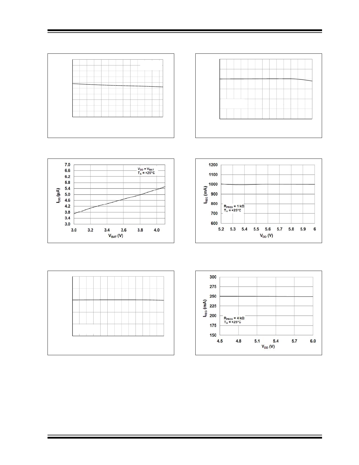
MCP73830/L
Note: Unless otherwise indicated, V
DD
= [V
REG
(Typical) + 1V], I
OUT
= 10 mA and T
A
= +25°C, Constant Voltage mode.
FIGURE 2-7:
Output Leakage Current
(I
DISCHARGE
) vs. Ambient Temperature (T
A
).
FIGURE 2-8:
Output Leakage Current
(I
DISCHARGE
) vs. Battery Regulation Voltage
(V
BAT
).
FIGURE 2-9:
Charge Current (I
OUT
) vs.
Ambient Temperature (T
A
), MCP73830.
FIGURE 2-10:
Charge Current (I
OUT
) vs.
Ambient Temperature (T
A
), MCP73830.
FIGURE 2-11:
Charge Current (I
OUT
) vs.
Supply Voltage (V
DD
), MCP73830.
FIGURE 2-12:
Charge Current (I
OUT
) vs.
Supply Voltage (V
DD
), MCP73830.
3 8
4.2
4.6
5.0
5.4
5.8
6.2
6.6
7.0
I
DIS
(µA)
V
DD
= V
REG
V
BAT
= 4.0V
3.0
3.4
3.8
-40 -30 -20 -10 0 10 20 30 40 50 60 70 80
Temp (°C)
900
1000
1100
1200
I
REG
(mA)
700
800
-45 -35 -25 -15 -5 5 15 25 35 45 55 65 75 85
Temp (°C)
V
DD
= 5.2V
R
PROG
= 1 k
200
225
250
275
300
I
REG
(mA)
V
DD
= 5.2V
R
4 k
150
175
-45 -35 -25 -15 -5 5 15 25 35 45 55 65 75 85
Temp (°C)
R
PROG
= 4 k
MCP73830/L
DS20005049D-page 8
2011-2014 Microchip Technology Inc.
3.0
PIN DESCRIPTION
The descriptions of the pins are listed in
Table 3-1
.
TABLE 3-1:
PIN FUNCTION TABLES
3.1
Battery Management 0V Reference
(V
SS
)
Connect to the negative terminal of the battery and
input supply.
3.2
Status Output (STAT)
STAT is an open-drain logic output for connection to an
LED for charge status indication in stand-alone
applications. Alternatively, a pull-up resistor can be
applied for interfacing to a host microcontroller. Refer to
Table 5-1
for a summary of the status output during a
charge cycle.
3.3
Battery Charge Control Output
(V
BAT
)
Connect to the positive terminal of the battery. Bypass
to V
SS
with a minimum of 1 µF to ensure loop stability
when the battery is disconnected.
3.4
Battery Management Input Supply
(V
DD
)
A supply voltage of [V
REG
(Typical) + 0.3V] to 6.0V is
recommended. Bypass to V
SS
with a minimum of 1 µF.
3.5
Charge Enable (CE)
The MCP73830/L is always enabled with an internal
pull-down resistor. Pulling the CE pin high will enter
Standby mode.
3.6
Current Regulation Set (PROG)
The fast charge current is set by placing a resistor from
PROG to V
SS
during Constant Current (CC) mode.
Refer to
Section 5.4 “Constant Current Mode – Fast
Charge”
for details.
3.7
Exposed Pad (EP)
The Exposed Thermal Pad (EP) should be connected
to the exposed copper area on the Printed Circuit
Board (PCB) for thermal enhancement purposes.
Additional vias on the copper area under the
MCP73830/L device can improve the performance of
heat dissipation and simplify the assembly process.
MCP73830/L
Symbol
I/O
Function
TDFN
1
V
SS
—
Battery management 0V reference.
2
STAT
O
Battery charge status output.
3
V
BAT
I/O
Charge control output. Regulates the charge current and battery voltage.
The pin is disconnected during Shutdown mode.
4
V
DD
I
Input power supply.
5
CE
I
Charge Enable pin. Pull the pin high to disable the device. It is internally
pulled down. Leave the pin float if not used.
6
PROG
I/O
Battery charge current regulation program.
7
EP
—
Exposed pad.
2011-2014 Microchip Technology Inc.
DS20005049D-page 9
MCP73830/L
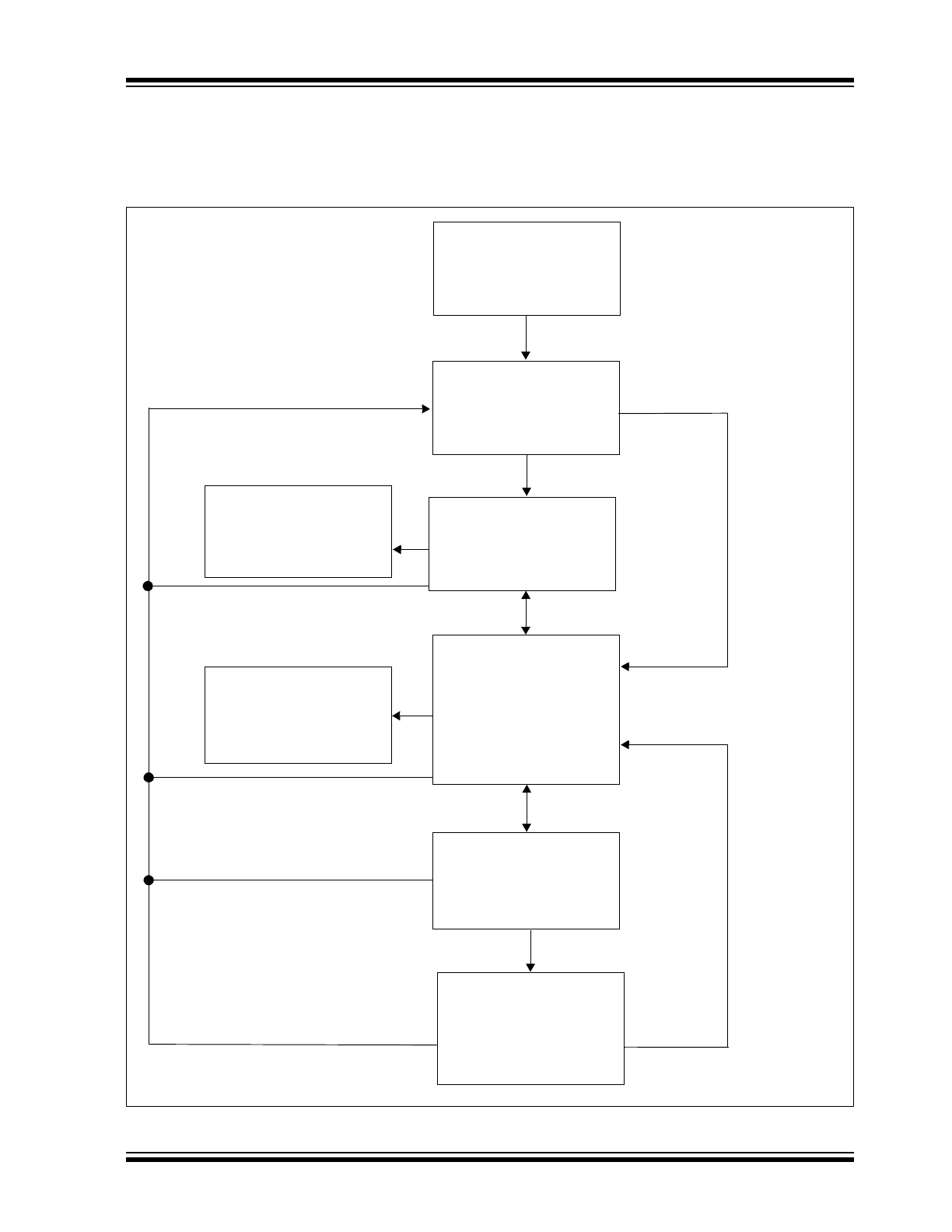
4.0
DEVICE OVERVIEW
The MCP73830/L are simple, but fully integrated, linear
charge management controllers.
Figure 4-1
depicts the
operational flow algorithm.
FIGURE 4-1:
The MCP73830/L Flowchart.
V
BAT
> V
PTH
*Continuously monitored
SHUTDOWN MODE
V
DD
< (UVLO)
V
DD
< (V
BAT
)*
V
BAT
> 96.5% V
REG
STAT = High Z
STANDBY MODE*
CE = High
STAT = High Z
PRECONDITIONING
MODE
Charge Current = I
REG
STAT = Low
PRE-TIMER FAULT
NO Charge Current
STAT = Flash (2 Hz)
Preconditioning Timer
Suspended
TIMER FAULT
NO Charge Current
STAT = High Z
Timer Suspended
CONSTANT CURRENT
MODE
Charge Current = I
PREG
STAT = Low
Preconditioning Timer
Suspended
Elapsed Timer Enabled
CONSTANT VOLTAGE
MODE
Charge Voltage = V
REG
STAT = Low
CHARGE COMPLETE
MODE
NO Charge Current
STAT = High Z
Timer Reset
V
BAT
= V
REG
V
BAT
>= V
PTH
V
BAT
< V
PTH
I
BAT
< I
TERM
V
BAT
< V
RTH
Recharge Mode
(available when selected device
has automatic recharge option).
CE = Low
CE = Low
No Auto-Recharge option
MCP73830/L
DS20005049D-page 10
2011-2014 Microchip Technology Inc.
5.0
DETAILED DESCRIPTION
5.1
Undervoltage Lockout (UVLO)
An Internal Undervoltage Lockout (UVLO) circuit
monitors the input voltage and keeps the charger in
Shutdown mode until the input supply rises above the
UVLO threshold. In the event a battery is present when
the input power is applied, the input supply must rise
approximately 150 mV above the battery voltage
before the MCP73830/L devices become operational.
The UVLO circuit places the device in Shutdown mode
if the input supply falls to approximately 150 mV above
the battery voltage. The UVLO circuit is always active.
Any time the input supply is below the UVLO threshold,
or approximately 150 mV of the voltage at the V
BAT
pin,
the MCP73830/L devices are placed in Shutdown
mode.
5.2
Charge Qualification
When the input power is applied, the input supply must
rise 150 mV above the battery voltage before the
MCP73830/L becomes operational.
The automatic power-down circuit places the device in
Shutdown mode if the input supply falls to within
+50 mV of the battery voltage.
The automatic circuit is always active. Any time the
input supply is within +50 mV of the voltage at the
V
BAT
pin, the MCP73830/L is placed in Shutdown
mode.
For a charge cycle to begin, the automatic power-
down conditions must be met, and the charge enable
input must be above the input high threshold. The
battery voltage should be less than 96.5% of V
REG
.
5.2.1
BATTERY MANAGEMENT INPUT
SUPPLY (V
DD
)
The V
DD
input is the input supply to the MCP73830/L.
The MCP73830/L automatically enters Power-Down
mode if the voltage on the V
DD
input falls to within
+50 mV of the battery voltage. This feature prevents
draining the battery pack when the V
DD
supply is not
present.
5.2.2
BATTERY CHARGE CONTROL
OUTPUT (V
BAT
)
The battery charge control output is the drain terminal
of an internal P-channel MOSFET. The MCP73830/L
provides constant current and voltage regulation to the
battery pack by controlling this MOSFET in the linear
region. The battery charge control output should be
connected to the positive terminal of the battery pack.
5.2.3
BATTERY DETECTION
The MCP73830/L device detects the battery presence
by monitoring the voltage at V
BAT
. The charge flow will
initiate when the voltage on V
BAT
is pulled below the
V
RECHARGE
threshold. Refer to
Section 1.0 “Electri-
cal Characteristics”
for V
RECHARGE
values. The value
will be the same for non-rechargeable devices.
When V
BAT
> V
REG
+ Hysteresis, the charge will be
suspended or not started, depending on the condition,
to prevent the overcharge that may occur.
5.3
Preconditioning
If the voltage at the V
BAT
pin is less than the precondi-
tioning threshold, the MCP73830/L devices enter
Preconditioning mode. The preconditioning threshold
is factory set. Refer to
Section 1.0 “Electrical Charac-
teristics”
for preconditioning threshold options.
In this mode, the MCP73830/L devices supply 10% of
the fast charge current (established with the value of
the resistor connected to the PROG pin) to the battery.
When the voltage at the V
BAT
pin rises above the pre-
conditioning threshold, the MCP73830/L device enters
the Constant Current (Fast Charge) mode.
5.3.1
TIMER EXPIRED DURING
PRECONDITIONING MODE
If the internal timer expires before the voltage threshold
is reached for Fast Charge mode, a timer fault is
indicated, and the charge cycle terminates. The
MCP73830/L devices remain in this condition until the
battery is removed, the input power is cycled, or CE is
toggled. If the battery is removed, the MCP73830/L
devices enter Standby mode, where they remain until a
battery is reinserted.
Note:
The MCP73830/L devices also offer
options with no preconditioning.
Note:
The typical preconditioning timers for the
MCP73830/L are 60 minutes.