
2009-2018 Microchip Technology Inc.
DS20002190D-page 1
MCP73213
Features
• Complete Linear Charge Management Controller:
- Integrated Input Overvoltage Protection
- Integrated Pass Transistor
- Integrated Current Sense
- Integrated Reverse Discharge Protection
• Constant Current/Constant Voltage Operation
with Thermal Regulation
• 4.15V Undervoltage Lockout (UVLO)
• 13V Input Overvoltage Protection
• High Accuracy Preset Voltage Regulation through
Full Temperature Range (–5°C to +55°C ±0.6%)
• Battery Charge Voltage Options:
- 8.20V, 8.40V, 8.7V or 8.8V
• Resistor Programmable Fast Charge Current:
- 130 mA-1100 mA
• Preconditioning of Deeply Depleted Cells:
- Available Options: 10% or Disable
• Integrated Precondition Timer:
- 32 Minutes or Disable
• Automatic End-of-Charge Control:
- Selectable Minimum Current Ratio:
5%, 7.5%, 10% or 20%
- Elapse Safety Timer: 4 hr., 6 hr., 8 hr.
or
Disable
• Automatic Recharge:
- Available Options: 95% or Disable
• Factory Preset Charge Status Output:
- On/Off or Flashing
• Soft Start
• Temperature Range: –40°C to +85°C
• Packaging: DFN-10 (3 mm x 3 mm)
Applications
• Digital Camcorders
• Portable Media Players
• Ultra Mobile Personal Computers
• Netbook Computers
• Handheld Devices
• Walkie-Talkie
• Low-Cost 2-Cell Li-Ion/Li-Poly Chargers/Cradles
Description
The MCP73213 is a highly integrated Li-Ion battery
charge management controller for use in space-limited
and cost-sensitive applications. The MCP73213
provides specific charge algorithms for dual-cell Li-Ion/
Li-Polymer batteries to achieve optimal capacity and
safety in the shortest charging time possible. Along
with its small physical size, the low number of external
components makes the MCP73213 ideally suitable for
portable applications. The absolute maximum voltage,
up to 18V, allows the use of MCP73213 in harsh
environments, such as low-cost wall wart or voltage
spikes from plug/unplug.
The MCP73213 employs a constant current/constant
voltage charge algorithm. The various charging voltage
regulations provide design engineers flexibility to use in
different applications. The fast charge, constant current
value is set with one external resistor from 130 mA to
1100 mA. The MCP73213 limits the charge current
based on die temperature during high-power or high-
ambient conditions. This thermal regulation optimizes
the charge cycle time while maintaining device
reliability.
The PROG pin of the MCP73213 also serves as enable
pin. When high impedance is applied, the MCP73213
will be in Standby mode.
The MCP73213 is fully specified over the ambient
temperature range of -40°C to +85°C. The MCP73213
is available in a 10-lead DFN package.
Package Types (Top View)
MCP73213
3x3 DFN *
V
BAT
V
DD
V
BAT
V
SS
V
SS
1
2
3
4
10
9
8
7 STAT
PROG
V
DD
* Includes Exposed Thermal Pad (EP); see
Table 3-1
.
EP
11
NC 5
6 NC
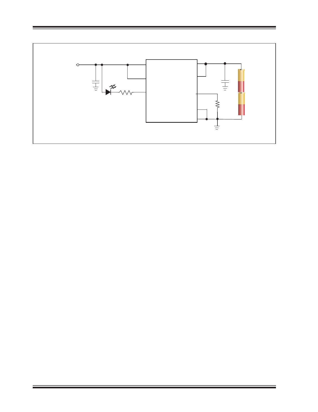
Dual-Cell Li-Ion/Li-Polymer Battery Charge Management
Controller with Input Overvoltage Protection
MCP73213
DS20002190D-page 2
2009-2018 Microchip Technology Inc.
Typical Application
V
DD
5
3
1
2
8
7
R
PROG
9
10
C
IN
C
OUT
R
LED
+
-
2-Cell
Li-Ion
Battery
6
4
MCP73213
V
DD
STAT
NC
NC
V
BAT
V
BAT
PROG
V
SS
V
SS
AC-DC-Adapter
2009-2018 Microchip Technology Inc.
DS20002190D-page
3
MCP73213
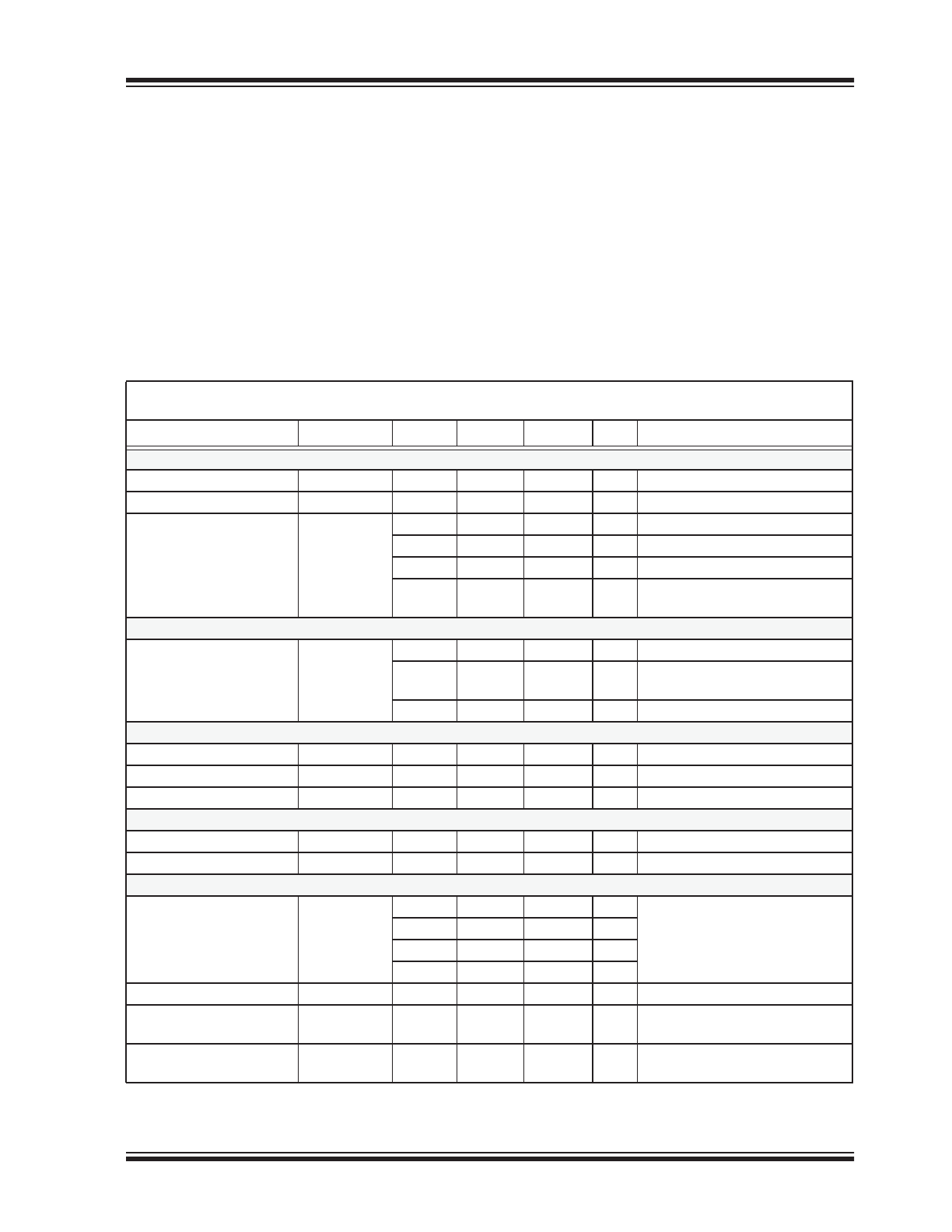
TABLE 1:
AVAILABLE FACTORY PRESET OPTIONS
TABLE 2:
STANDARD SAMPLE OPTIONS
Charge
Voltage
OVP
Preconditioning
Charge Current
Preconditioning
Threshold
Precondition
Timer
Elapse
Timer
End-of-Charge
Control
Automatic
Recharge
Output
Status
8.2V
13V
Disable/10%
66.5%/71.5%
Disable/
32 Minimum
Disable/4 hr/
6 hr/8 hr
5%/7.5%/
10%/20%
No/
Yes
Type 1/
Type 2
8.4V
13V
Disable/10%
66.5%/71.5%
Disable/
32 Minimum
Disable/4 hr/
6 hr/8 hr
5%/7.5%/
10%/20%
No/
Yes
Type 1/
Type 2
8.7V
13V
Disable/10%
66.5%/71.5%
Disable/
32 Minimum
Disable/4 hr/
6 hr/8 hr
5%/7.5%/
10%/20%
No/
Yes
Type 1/
Type 2
8.8V
13V
Disable/10%
66.5%/71.5%
Disable/
32 Minimum
Disable/4 hr/
6 hr/8 hr
5%/7.5%/
10%/20%
No/
Yes
Type 1/
Type 2
Note 1:
I
REG
: Regulated fast charge current.
2:
V
REG
: Regulated charge voltage.
3:
I
PREG
/I
REG
: Preconditioning charge current; ratio of regulated fast charge current.
4:
I
TERM
/I
REG
: End-of-Charge control; ratio of regulated fast charge current.
5:
V
RTH
/V
REG
: Recharge threshold; ratio of regulated battery voltage.
6:
V
PTH
/V
REG
: Preconditioning threshold voltage.
7:
Type 1: On/Off; Type 2: Flashing. Please refer to
Table 5-2
.
Part
Number
V
REG
OVP
I
PREG
/I
REG
Precharge
Timer
Elapse
Timer
I
TERM
/I
REG
V
RTH
/V
REG
V
PTH
/V
REG
Output
Status
MCP73213-B6S/MF
8.20V
13V
10%
32 Minimum
6 hr
10%
95%
71.5%
Type 1
MCP73213-A6S/MF
8.40V
13V
10%
32 Minimum
6 hr
10%
95%
71.5%
Type 1
Note 1:
Customers should contact their distributor, representatives or field application engineer (FAE) for support and sample. Local sales offices are also avail-
able to help customers. A listing of sales offices and locations is included at the back of this document. Technical support is available through the web site
at:
http://www.microchip.com/support
MCP73213
DS20002190D-page 4
2009-2018 Microchip Technology Inc.
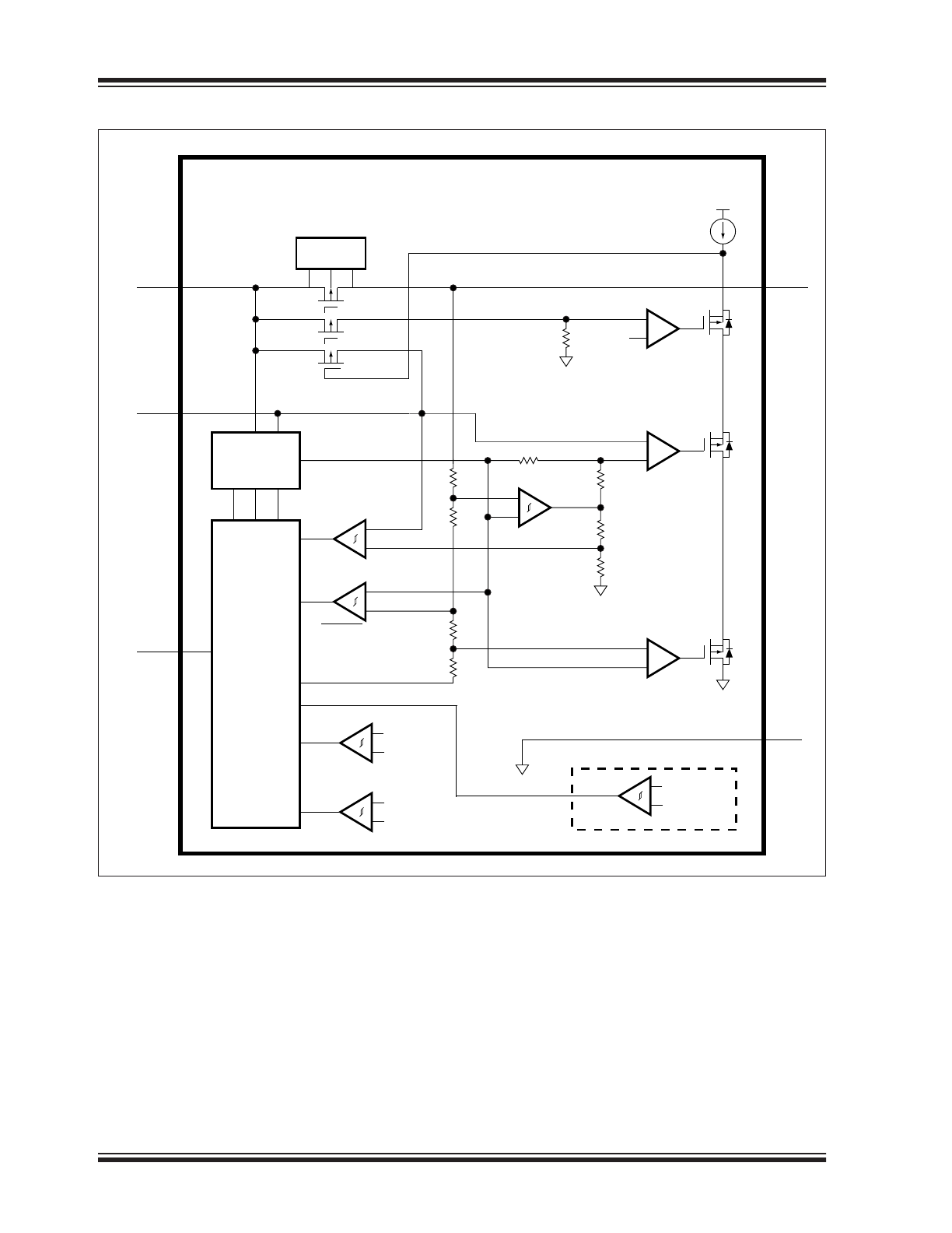
Functional Block Diagram
REFERENCE,
BIAS, UVLO,
AND SHDN
VREF (1.21V)
STAT
PROG
VBAT
VSS
DIRECTION
CONTROL
PRECONDITION
+
-
TERM
+
-
+
-
CA
CHARGE
+
-
+
-
VA
+
-
CURRENT
LIMIT
CHARGE
CONTROL,
TIMER,
AND
STATUS
LOGIC
VREF
VOREG
VOREG
UVLO
VDD
Input OverVP
VDD
+
-
13V
Thermal Regulation
TSD
+
-
110
°C
*Recharge
VBAT
+
-
95% VREG
*Only available on selected options
G=0.001
2009-2018 Microchip Technology Inc.
DS20002190D-page 5
MCP73213
1.0
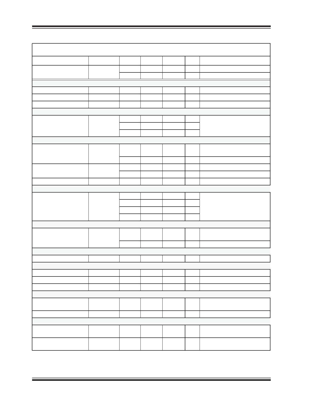
ELECTRICAL
CHARACTERISTICS
Absolute Maximum Ratings†
V
DD
......................................................................18.0V
V
PROG
...................................................................6.0V
All Inputs and Outputs w.r.t. V
SS
.....-0.3 to (V
DD
+0.3)V
Maximum Junction Temperature, T
J
. Internally Limited
Storage Temperature ........................ –65°C to +150°C
ESD Protection on All Pins
4 kV HBM
ESD Protection on All Pins
300V MM
† Notice:
Stresses above those listed under “Maximum
Ratings” may cause permanent damage to the device.
This is a stress rating only and functional operation of
the device at those or any other conditions above those
indicated in the operational listings of this specification
is not implied. Exposure to maximum rating conditions
for extended periods may affect device reliability.
DC CHARACTERISTICS
Electrical Specifications:
Unless otherwise indicated, all limits apply for V
DD
= [V
REG
(Typical) + 0.3V] to 12V,
T
A
= -40°C to +85°C. Typical values are at +25°C, V
DD
= [V
REG
(Typical) + 1.0V]
Parameters
Sym.
Min.
Typ.
Max.
Units
Conditions
Supply Input
Input Voltage Range
V
DD
4
—
16
V
Operating Supply Voltage
V
DD
4.2
—
13
V
Supply Current
I
SS
—
4
5.5
μA
Shutdown (V
DD
≤ V
BAT
– 150 mV)
—
700
1500
μA
Charging
—
50
125
μA
Standby (PROG Floating)
—
50
150
μA
Charge Complete; No Battery;
V
DD
< V
STOP
Battery Discharge Current
Output Reverse Leakage
Current
I
DISCHARGE
—
0.5
2
μA
Standby (PROG Floating)
—
0.5
2
μA
Shutdown (V
DD
≤ V
BAT
or V
DD
< V
STOP
)
—
10
17
μA
Charge Complete; V
DD
is present
Undervoltage Lockout
UVLO Start Threshold
V
START
4.10
4.15
4.25
V
UVLO Stop Threshold
V
STOP
4.00
4.05
4.10
V
UVLO Hysteresis
V
HYS
—
100
—
mV
Overvoltage Protection
OVP Start Threshold
V
OVP
12.8
13
13.2
V
OVP Hysteresis
V
OVPHYS
—
150
—
mV
Voltage Regulation (Constant Voltage Mode)
Regulated Output Voltage
Options
V
REG
8.15
8.20
8.25
V
T
A
= –5°C to +55°C
V
DD
= [V
REG
(Typical)+1V]
I
OUT
= 50 mA
8.35
8.40
8.45
V
8.65
8.70
8.75
V
8.75
8.80
8.85
V
Output Voltage Tolerance
V
RTOL
–0.6
—
0.6
%
Line Regulation
V
BAT
/
V
BAT
)/
V
DD
|
—
0.05
0.20
%/V V
DD
= [V
REG
(Typical)+1V] to 12V
I
OUT
= 50 mA
Load Regulation
V
BAT
/V
BAT
|
—
0.05
0.20
%
I
OUT
= 50 mA – 150 mA
V
DD
= [V
REG
(Typical)+1V]
Note 1:
Not production tested. Ensured by design.
MCP73213
DS20002190D-page 6
2009-2018 Microchip Technology Inc.
Supply Ripple Attenuation
PSRR
—
–46
—
dB
I
OUT
= 20 mA, 10 Hz to 1 kHz
—
–30
—
dB
I
OUT
= 20 mA, 10 Hz to 10 kHz
Battery Short Protection
BSP Start Threshold
V
SHORT
—
3.4
—
V
BSP Hysteresis
V
BSPHYS
—
150
—
mV
BSP Regulation Current
I
SHORT
—
25
—
mA
Current Regulation (Fast Charge, Constant-Current Mode)
Fast Charge Current
Regulation
I
REG
130
—
1100
mA
T
A
= –5°C to +55°C
PROG = 10 k
PROG = 1.1 k
117
130
143
mA
900
1000
1100
mA
Preconditioning Current Regulation (Trickle Charge Constant-Current Mode)
Precondition Current
Ratio
I
PREG
/I
REG
—
10
—
%
PROG = 1 k
to 10 k
T
A
=-5°C to +55°C
—
100
—
%
No Preconditioning
Precondition Voltage
Threshold Ratio
V
PTH
/V
REG
64
66.5
69
%
V
BAT
Low-to-High
69
71.5
74
%
V
BAT
Low-to-High
Precondition Hysteresis
V
PHYS
—
100
—
mV
V
BAT
High-to-Low (
Note 1
)
Charge Termination
Charge Termination
Current Ratio
I
TERM
/I
REG
3.7
5
6.3
%
PROG = 1 k
to 10 k
T
A
=–5°C to +55°C
5.6
7.5
9.4
%
7.5
10
12.5
%
15
20
25
%
Automatic Recharge
Recharge Voltage
Threshold Ratio
V
RTH
/V
REG
93
95.0
97
%
V
BAT
High-to-Low
—
0
—
%
No Automatic Recharge
Pass Transistor ON-Resistance
ON-Resistance
R
DSON
—
350
—
m
V
DD
= 4.5V, T
J
= 105°C (
Note 1
)
Status Indicator - STAT
Sink Current
I
SINK
—
20
35
mA
Low Output Voltage
V
OL
—
0.2
0.5
V
I
SINK
= 4 mA
Input Leakage Current
I
LK
—
0.001
1
μA
High Impedance, V
DD
on pin
PROG Input
Charge Impedance
Range
R
PROG
1
—
22
k
Shutdown Impedance
R
PROG
—
200
—
k
Impedance for Shutdown
Automatic Power-Down
Automatic Power-Down
Entry Threshold
V
PDENTRY
V
BAT
+ 10
mV
V
BAT
+ 50
mV
—
V
V
DD
Falling
Automatic Power-Down
Exit Threshold
V
PDEXIT
—
V
BAT
+ 150
mV
V
BAT
+ 250
mV
V
V
DD
Rising
DC CHARACTERISTICS
(CONTINUED)
Electrical Specifications:
Unless otherwise indicated, all limits apply for V
DD
= [V
REG
(Typical) + 0.3V] to 12V,
T
A
= -40°C to +85°C. Typical values are at +25°C, V
DD
= [V
REG
(Typical) + 1.0V]
Parameters
Sym.
Min.
Typ.
Max.
Units
Conditions
Note 1:
Not production tested. Ensured by design.
2009-2018 Microchip Technology Inc.
DS20002190D-page 7
MCP73213
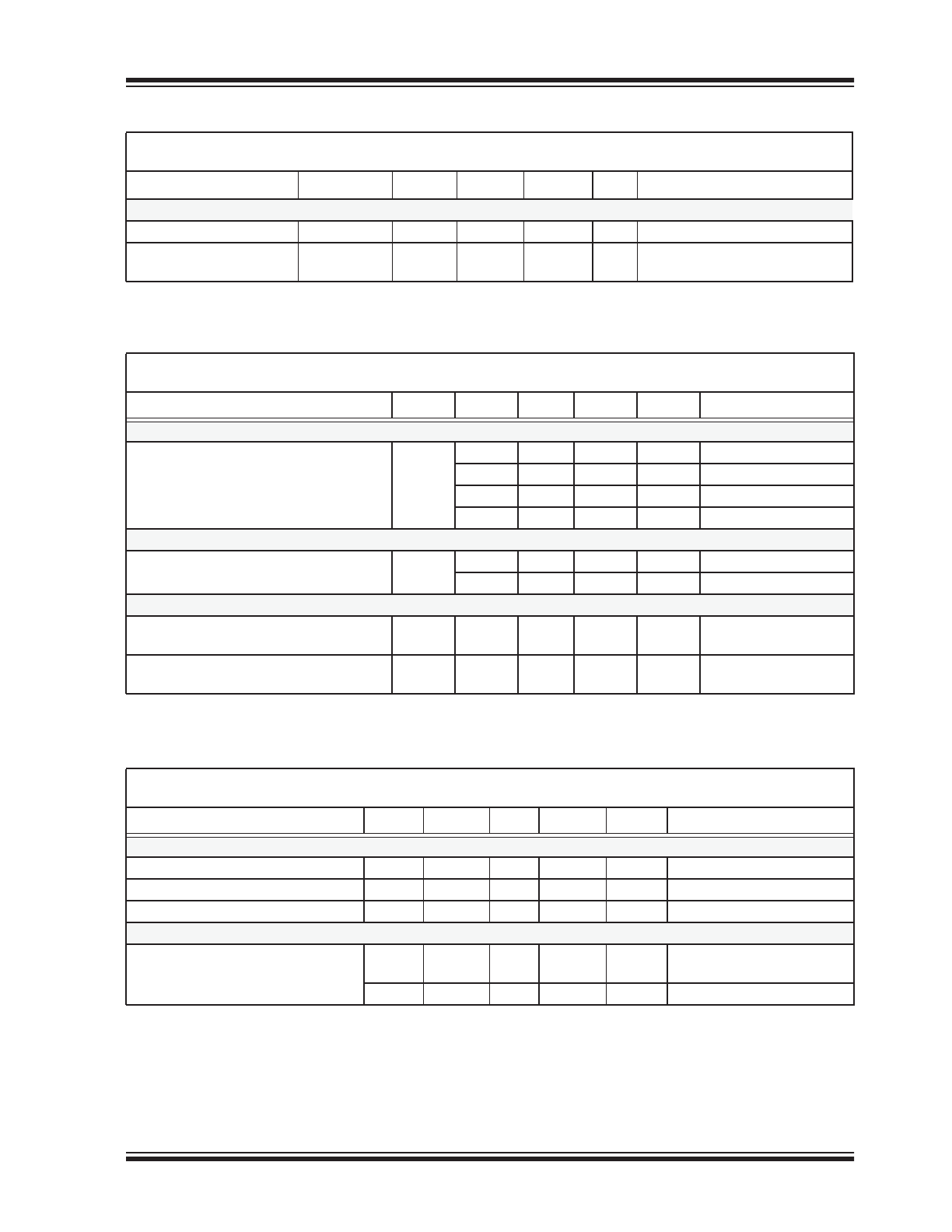
AC CHARACTERISTICS
TEMPERATURE SPECIFICATIONS
Thermal Shutdown
Die Temperature
T
SD
—
150
—
C
Die Temperature
Hysteresis
T
SDHYS
—
10
—
C
Electrical Specifications:
Unless otherwise specified, all limits apply for V
DD
= [V
REG
(Typical)+0.3V] to 12V,
T
A
=–40°C to +85°C. Typical values are at +25°C, V
DD
= [V
REG
(Typical)+1.0V]
Parameters
Sym.
Min.
Typ.
Max.
Units
Conditions
Elapsed Timer
Elapsed Timer Period
t
EL-
APSED
—
0
—
Hours
Timer Disabled
3.6
4.0
4.4
Hours
5.4
6.0
6.6
Hours
7.2
8.0
8.8
Hours
Preconditioning Timer
Preconditioning Timer Period
t
PRECHG
—
0
—
Hours
Disabled Timer
0.4
0.5
0.6
Hours
Status Indicator
Status Output Turn-Off
t
OFF
—
—
500
μs
I
SINK
= 1 mA to 0 mA
(
Note 1
)
Status Output Turn-On
t
ON
—
—
500
μs
I
SINK
= 0 mA to 1 mA
(
Note 1
)
Note 1:
Not production tested. Ensured by design.
Electrical Specifications:
Unless otherwise indicated, all limits apply for V
DD
= [V
REG
(Typical) + 0.3V] to 6V.
Typical values are at +25°C, V
DD
= [V
REG
(Typical) + 1.0V]
Parameters
Sym.
Min.
Typ.
Max.
Units
Conditions
Temperature Ranges
Specified Temperature Range
T
A
–40
—
+85
°C
Operating Temperature Range
T
J
–40
—
+125
°C
Storage Temperature Range
T
A
–65
—
+150
°C
Thermal Package Resistances
Thermal Resistance, DFN-10LD
(3x3)
JA
—
62
—
°C/W
4-Layer JC51-7 Standard
Board, Natural Convection
JC
—
20.5
—
°C/W
DC CHARACTERISTICS
(CONTINUED)
Electrical Specifications:
Unless otherwise indicated, all limits apply for V
DD
= [V
REG
(Typical) + 0.3V] to 12V,
T
A
= -40°C to +85°C. Typical values are at +25°C, V
DD
= [V
REG
(Typical) + 1.0V]
Parameters
Sym.
Min.
Typ.
Max.
Units
Conditions
Note 1:
Not production tested. Ensured by design.

MCP73213
DS20002190D-page 8
2009-2018 Microchip Technology Inc.
NOTES:
2009-2018 Microchip Technology Inc.
DS20002190D-page 9
MCP73213
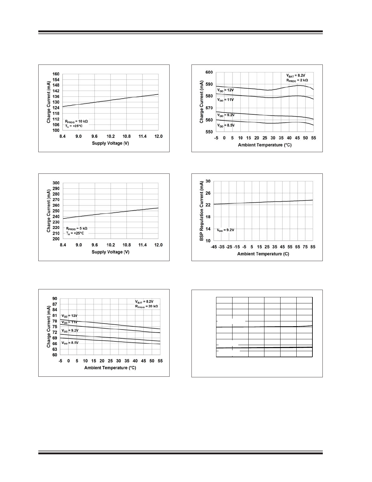
2.0
TYPICAL PERFORMANCE CURVES
Note:
Unless otherwise indicated, V
DD
= [V
REG
(Typical) + 1V], T
A
= +25°C, Constant Voltage mode.
FIGURE 2-1:
Battery Regulation Voltage
(V
BAT
) vs. Supply Voltage (V
DD
).
FIGURE 2-2:
Battery Regulation Voltage
(V
BAT
) vs. Supply Voltage (V
DD
).
FIGURE 2-3:
Battery Regulation Voltage
(V
BAT
) vs. Ambient Temperature (T
A
).
FIGURE 2-4:
Battery Regulation Voltage
(V
BAT
) vs. Ambient Temperature (T
A
).
FIGURE 2-5:
Charge Current (I
OUT
) vs.
Programming Resistor (R
PROG
).
FIGURE 2-6:
Charge Current (I
OUT
) vs.
Supply Voltage (V
DD
).
Note:
The graphs and tables provided following this note are a statistical summary based on a limited number of
samples and are provided for informational purposes only. The performance characteristics listed herein
are not tested or guaranteed. In some graphs or tables, the data presented may be outside the specified
operating range (e.g., outside specified power supply range) and therefore outside the warranted range.
MCP73213
DS20002190D-page 10
2009-2018 Microchip Technology Inc.
TYPICAL PERFORMANCE CURVES
(CONTINUED)
Note:
Unless otherwise indicated, V
DD
= [V
REG
(Typical) + 1V], T
A
= +25°C, Constant-voltage mode.
FIGURE 2-7:
Charge Current (I
OUT
) vs.
Supply Voltage (V
DD
).
FIGURE 2-8:
Charge Current (I
OUT
) vs.
Supply Voltage (V
DD
).
FIGURE 2-9:
Charge Current (I
OUT
) vs.
Ambient Temperature (T
A
).
FIGURE 2-10:
Charge Current (I
OUT
) vs.
Ambient Temperature (T
A
).
FIGURE 2-11:
Battery Short Protection
Regulation Current (I
SHORT
) vs. Ambient
Temperature (T
A
).
FIGURE 2-12:
Output Leakage Current
(I
DISCHARGE
) vs. Ambient Temperature (T
A
).
-1.0
0.0
1.0
2.0
3.0
4.0
5.0
6.0
7.0
8.0
9.0
-5.0
5.0
15.0
25.0
35.0
45.0
55.0
Discharge Current (µA)
Ambient Temperature (°C)
V
DD
< V
BAT
V
DD
< V
STOP
End of Charge