
2015 Microchip Technology Inc.
DS20005385B-page 1
MCP6V71/1U/2/4
Features
• High DC Precision:
- V
OS
Drift: ±15 nV/°C (maximum, V
DD
= 5.5V)
- V
OS
: ±8 µV (maximum)
- A
OL
: 126 dB (minimum, V
DD
= 5.5V)
- PSRR: 115 dB (minimum, V
DD
= 5.5V)
- CMRR: 117 dB (minimum, V
DD
= 5.5V)
- E
ni
: 0.45 µV
P-P
(typical), f = 0.1 Hz to 10 Hz
- E
ni
: 0.15 µV
P-P
(typical), f = 0.01 Hz to 1 Hz
• Enhanced EMI Protection:
- Electromagnetic Interference Rejection Ratio
(EMIRR) at 1.8 GHz: 96 dB
• Low Power and Supply Voltages:
- I
Q
: 170 µA/amplifier (typical)
- Wide Supply Voltage Range: 2V to 5.5V
• Small Packages:
- Singles in SC70, SOT-23
- Duals in MSOP-8, 2x3 TDFN
- Quads in TSSOP-14
• Easy to Use:
- Rail-to-Rail Input/Output
- Gain Bandwidth Product: 2 MHz (typical)
- Unity Gain Stable
• Extended Temperature Range: -40°C to +125°C
Typical Applications
• Portable Instrumentation
• Sensor Conditioning
• Temperature Measurement
• DC Offset Correction
• Medical Instrumentation
Design Aids
• FilterLab
®
Software
• Microchip Advanced Part Selector (MAPS)
• Analog Demonstration and Evaluation Boards
• Application Notes
Related Parts
• MCP6V11/1U/2/4: Zero-Drift, Low Power
• MCP6V31/1U/2/4
• MCP6V61/1U: Zero-Drift 1 MHz
• MCP6V81/1U: Zero-Drift, 5 MHz
•
MCP6V91/1U: Zero-Drift, 10 MHz
Description
The Microchip Technology Inc. MCP6V71/1U/2/4
family of operational amplifiers provides input offset
voltage correction for very low offset and offset drift.
These are low-power devices with a gain bandwidth
product of 2 MHz (typical). They are unity-gain stable,
have virtually no 1/f noise and have good Power Supply
Rejection Ratio (PSRR) and Common Mode Rejection
Ratio (CMRR). These products operate with a single
supply voltage as low as 2V, while drawing
170 µA/amplifier (typical) of quiescent current.
The MCP6V71/1U/2/4 family has enhanced EMI pro-
tection to minimize any electromagnetic interference
from external sources. This feature makes it well suited
for EMI sensitive applications such as power lines,
radio stations and mobile communications, etc.
The Microchip Technology Inc. MCP6V71/1U/2/4 op
amps are offered in single (MCP6V71 and
MCP6V71U), dual (MCP6V72) and quad (MCP6V74)
packages. They were designed using an advanced
CMOS process.
Package Types
V
IN
+
V
SS
V
IN
–
1
2
3
5
4
V
DD
V
OUT
MCP6V71
SOT-23
MCP6V71U
SC70, SOT-23
V
IN
–
V
SS
V
OUT
1
2
3
5
4
V
DD
V
IN
+
V
INA
+
V
INA
–
V
SS
1
2
3
4
8
7
6
5
V
OUTA
V
DD
V
OUTB
V
INB
–
V
INB
+
MCP6V72
MSOP
MCP6V72
2×3 TDFN *
V
INA
+
V
INA
–
V
SS
V
OUTB
V
INB
–
1
2
3
4
8
7
6
5 V
INB
+
V
DD
V
OUTA
EP
9
* Includes Exposed Thermal Pad (EP); see
Table 3-1
.
V
INA
+
V
INA
–
V
DD
1
2
3
4
14
13
12
11
V
OUTA
V
OUTD
V
IND
–
V
IND
+
V
SS
MCP6V74
TSSOP
V
INB
–
V
INB
+
V
OUTB
5
6
7
10
9
8
V
INC
+
V
INC
–
V
OUTC
170 µA, 2 MHz Zero-Drift Op Amps
MCP6V71/1U/2/4
DS20005385B-page 2
2015 Microchip Technology Inc.
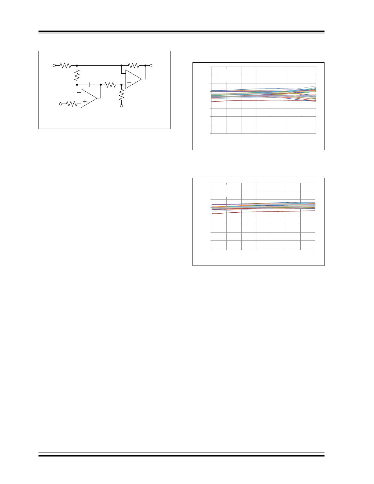
Typical Application Circuit
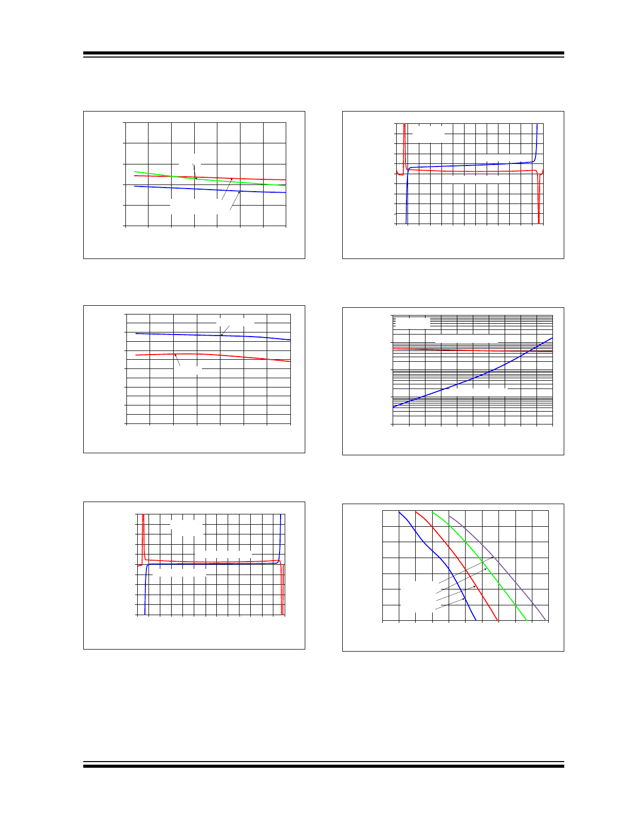
Figures 1
and
2
show input offset voltage versus ambi-
ent temperature for different power supply voltages.
FIGURE 1:
Input Offset Voltage vs.
Temperature with V
DD
= 2V.
FIGURE 2:
Input Offset Voltage vs.
Temperature with V
DD
= 5.5V.
As seen in
Figures 1
and
2
, the MCP6V71/1U/2/4 op
amps have excellent performance across temperature.
The input offset voltage temperature drift (TC
1
) shown
is well within the specified maximum values of
15 nV/°C at V
DD
= 5.5V and 30 nV/°C at V
DD
= 2V.
This performance supports applications with stringent
DC precision requirements. In many cases, it will not be
necessary to correct for temperature effects (i.e.,
calibrate) in a design. In the other cases, the correction
will be small.
U
1
MCP6XXX
Offset Voltage Correction for Power Driver
C
2
R
2
R
1
R
3
V
DD
/2
R
4
V
IN
V
OUT
R
2
V
DD
/2
R
5
U
2
MCP6V71
-8
-6
-4
-2
0
2
4
6
8
-50
-25
0
25
50
75
100
125
Input Offset V
o
ltage
(µV)
Ambient Temperature (°C)
28 Samples
V
DD
= 2V
-8
-6
-4
-2
0
2
4
6
8
-50
-25
0
25
50
75
100
125
Input Offset V
o
ltage
(µV)
Ambient Temperature (°C)
28 Samples
V
DD
= 2V
28 Samples
V
DD
= 5.5V
2015 Microchip Technology Inc.
DS20005385B-page 3
MCP6V71/1U/2/4
1.0
ELECTRICAL
CHARACTERISTICS
1.1
Absolute Maximum Ratings †
V
DD
– V
SS
.................................................................................................................................................................6.5V
Current at Input Pins ..............................................................................................................................................±2 mA
Analog Inputs (V
IN
+ and V
IN
-) (
Note 1
)
......................................................................................V
SS
– 1.0V to V
DD
+1.0V
All Other Inputs and Outputs ......................................................................................................V
SS
– 0.3V to V
DD
+0.3V
Difference Input Voltage .................................................................................................................................|V
DD
– V
SS
|
Output Short Circuit Current ........................................................................................................................... Continuous
Current at Output and Supply Pins ......................................................................................................................±30 mA
Storage Temperature .............................................................................................................................-65°C to +150°C
Maximum Junction Temperature .......................................................................................................................... +150°C
ESD protection on all pins (HBM, CDM, MM)
MCP6V71/1U
4 kV, 1.5 kV, 400V
MCP6V72/4
4 kV, 1.5 kV, 300V
Note 1:
See
Section 4.2.1, Rail-to-Rail Inputs
.
1.2
Specifications
† Notice:
Stresses above those listed under “Absolute Maximum Ratings” may cause permanent damage to the
device. This is a stress rating only, and functional operation of the device at those or any other conditions above those
indicated in the operational listings of this specification is not implied. Exposure to maximum rating conditions for
extended periods may affect device reliability.
TABLE 1-1:
DC ELECTRICAL SPECIFICATIONS
Electrical Characteristics:
Unless otherwise indicated, T
A
= +25°C, V
DD
= +2V to +5.5V, V
SS
= GND,
V
CM
= V
DD
/3,V
OUT
= V
DD
/2, V
L
= V
DD
/2, R
L
= 20 kΩ to V
L
and C
L
= 30 pF (refer to
Figures 1-4
and
1-5
).
Parameters
Sym.
Min.
Typ.
Max.
Units
Conditions
Input Offset
Input Offset Voltage
V
OS
-8
—
+8
µV
T
A
= +25°C
Input Offset Voltage Drift with
Temperature (Linear Temp. Co.)
TC
1
-30
—
+30
nV/°C T
A
= -40 to +125°C,
V
DD
= 2V (
Note 1
)
-15
—
+15
T
A
= -40 to +125°C,
V
DD
= 5.5V (
Note 1
)
Input Offset Voltage Quadratic
Temp. Co.
TC
2
—
-30
—
pV/°C
2
T
A
= -40 to +125°C,
V
DD
= 2V
—
-6
—
T
A
= -40 to +125°C,
V
DD
= 5.5V (
Note 1
)
Input Offset Voltage Aging
∆V
OS
—
±0.75
—
µV
408 hours Life Test at
+150°,
measured at +25°C
Power Supply Rejection Ratio
PSRR
115
125
—
dB
Note 1:
For Design Guidance only; not tested.
2:
Figure 2-19
shows how V
CML
and V
CMH
changed across temperature for the first production lot.
3:
Parts with date codes prior to September 2015 (week code 27) were screened to a +3 nA maximum limit.
4:
Parts with date codes prior to September 2015 (week code 27) were screened to ±1 nA minimum/maxi-
mum limits.
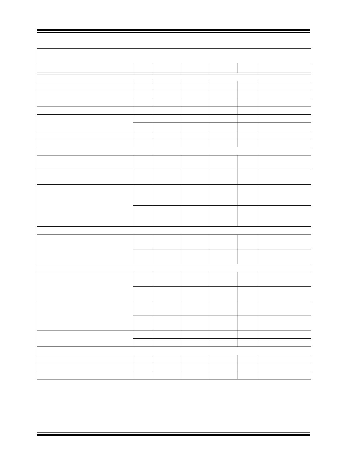
MCP6V71/1U/2/4
DS20005385B-page 4
2015 Microchip Technology Inc.
Input Bias Current and Impedance
Input Bias Current
I
B
-50
±1
+50
pA
Input Bias Current across
Temperature
I
B
—
+20
—
pA
T
A
= +85°C
I
B
0
+0.2
+1.5
nA
T
A
= +125°C (
Note 3
)
Input Offset Current
I
OS
-250
±60
+250
pA
Input Offset Current across
Temperature
I
OS
—
±50
—
pA
T
A
= +85°C
I
OS
-800
±50
+800
pA
T
A
= +125°C (
Note 4
)
Common Mode Input Impedance
Z
CM
—
10
13
||6
—
Ω||pF
Differential Input Impedance
Z
DIFF
—
10
13
||6
—
Ω||pF
Common Mode
Common Mode
Input Voltage Range Low
V
CML
—
—
V
SS
0.2
V
(
Note 2
)
Common Mode
Input Voltage Range High
V
CMH
V
DD
+ 0.3
—
—
V
(
Note 2
)
Common Mode Rejection Ratio
CMRR
111
122
—
dB
V
DD
= 2V,
V
CM
= -0.2V to 2.3V
(
Note 2
)
CMRR
117
130
—
dB
V
DD
= 5.5V,
V
CM
= -0.2V to 5.8V
(
Note 2
)
Open-Loop Gain
DC Open-Loop Gain (large signal)
A
OL
117
132
—
dB
V
DD
= 2V,
V
OUT
= 0.3V to 1.8V
A
OL
126
137
—
dB
V
DD
= 5.5V,
V
OUT
= 0.3V to 5.3V
Output
Minimum Output Voltage Swing
V
OL
V
SS
V
SS
+ 35 V
SS
+ 121
mV
R
L
= 2 kΩ, G = +2,
0.5V input overdrive
V
OL
—
V
SS
+ 3.5
—
mV
R
L
= 20 kΩ, G = +2,
0.5V input overdrive
Maximum Output Voltage Swing
V
OH
V
DD
– 121 V
DD
– 45
V
DD
mV
R
L
= 2 kΩ, G = +2,
0.5V input overdrive
V
OH
—
V
DD
– 4.5
—
mV
R
L
= 20 kΩ, G = +2,
0.5V input overdrive
Output Short Circuit Current
I
SC
—
±9
—
mA
V
DD
= 2V
I
SC
—
±26
—
mA
V
DD
= 5.5V
Power Supply
Supply Voltage
V
DD
2
—
5.5
V
Quiescent Current per Amplifier
I
Q
100
170
260
µA
I
O
= 0
POR Trip Voltage
V
POR
0.9
1.2
1.6
V
TABLE 1-1:
DC ELECTRICAL SPECIFICATIONS (CONTINUED)
Electrical Characteristics:
Unless otherwise indicated, T
A
= +25°C, V
DD
= +2V to +5.5V, V
SS
= GND,
V
CM
= V
DD
/3,V
OUT
= V
DD
/2, V
L
= V
DD
/2, R
L
= 20 kΩ to V
L
and C
L
= 30 pF (refer to
Figures 1-4
and
1-5
).
Parameters
Sym.
Min.
Typ.
Max.
Units
Conditions
Note 1:
For Design Guidance only; not tested.
2:
Figure 2-19
shows how V
CML
and V
CMH
changed across temperature for the first production lot.
3:
Parts with date codes prior to September 2015 (week code 27) were screened to a +3 nA maximum limit.
4:
Parts with date codes prior to September 2015 (week code 27) were screened to ±1 nA minimum/maxi-
mum limits.
2015 Microchip Technology Inc.
DS20005385B-page 5
MCP6V71/1U/2/4
TABLE 1-2:
AC ELECTRICAL SPECIFICATIONS
Electrical Characteristics:
Unless otherwise indicated, T
A
= +25°C, V
DD
= +2V to +5.5V, V
SS
= GND,
V
CM
= V
DD
/3, V
OUT
= V
DD
/2, V
L
= V
DD
/2, R
L
= 20 kΩ to V
L
and C
L
= 30 pF (refer to
Figure 1-4
and
Figure 1-5
).
Parameters
Sym.
Min.
Typ.
Max.
Units
Conditions
Amplifier AC Response
Gain Bandwidth Product
GBWP
—
2
—
MHz
Slew Rate
SR
—
1.0
—
V/µs
Phase Margin
PM
—
60
—
°
G = +1
Amplifier Noise Response
Input Noise Voltage
E
ni
—
0.15
—
µV
P-P
f = 0.01 Hz to 1 Hz
E
ni
—
0.45
—
µV
P-P
f = 0.1 Hz to 10 Hz
Input Noise Voltage Density
e
ni
—
21
—
nV/√Hz f < 2 kHz
Input Noise Current Density
i
ni
—
5
—
fA/√Hz
Amplifier Distortion (
Note 1
)
Intermodulation Distortion (AC)
IMD
—
11
—
µV
PK
V
CM
tone = 100 mV
PK
at 1 kHz, G
N
= 1
Amplifier Step Response
Start Up Time
t
STR
—
200
—
µs
G = +1, 0.1% V
OUT
settling (
Note 2
)
Offset Correction Settling Time
t
STL
—
15
—
µs
G = +1, V
IN
step of 2V,
V
OS
within 100 µV of its final value
Output Overdrive Recovery Time
t
ODR
—
40
—
µs
G = -10, ±0.5V input overdrive to V
DD
/2,
V
IN
50% point to V
OUT
90% point (
Note 3
)
EMI Protection
EMI Rejection Ratio
EMIRR
—
75
—
dB
V
IN
= 0.1 V
PK
, f = 400 MHz
—
89
—
V
IN
= 0.1 V
PK
, f = 900 MHz
—
96
—
V
IN
= 0.1 V
PK
, f = 1800 MHz
—
98
—
V
IN
= 0.1 V
PK
, f = 2400 MHz
Note 1:
These parameters were characterized using the circuit in
Figure 1-6
. In
Figures 2-40
and
2-41
, there is
an IMD tone at DC, a residual tone at 1 kHz and other IMD tones and clock tones.
2:
High gains behave differently; see
Section 4.3.3, Offset at Power Up
.
3:
t
ODR
includes some uncertainty due to clock edge timing.
TABLE 1-3:
TEMPERATURE SPECIFICATIONS
Electrical Characteristics:
Unless otherwise indicated, all limits are specified for: V
DD
= +2V to +5.5V, V
SS
= GND.
Parameters
Sym.
Min.
Typ.
Max.
Units
Conditions
Temperature Ranges
Specified Temperature Range
T
A
-40
—
+125
°C
Operating Temperature Range
T
A
-40
—
+125
°C
(
Note 1
)
Storage Temperature Range
T
A
-65
—
+150
°C
Thermal Package Resistances
Thermal Resistance, 5L-SC-70
JA
—
209
—
°C/W
Thermal Resistance, 5L-SOT-23
JA
—
201
—
°C/W
Thermal Resistance, 8L-2x3 TDFN
JA
—
53
—
°C/W
Thermal Resistance, 8L-MSOP
JA
—
211
—
°C/W
Thermal Resistance, 14L-TSSOP
JA
—
100
—
°C/W
Note 1:
Operation must not cause T
J
to exceed Maximum Junction Temperature specification (+150°C).
MCP6V71/1U/2/4
DS20005385B-page 6
2015 Microchip Technology Inc.
1.3
Timing Diagrams
FIGURE 1-1:
Amplifier Start Up.
FIGURE 1-2:
Offset Correction Settling
Time.
FIGURE 1-3:
Output Overdrive Recovery.
1.4
Test Circuits
The circuits used for most DC and AC tests are shown
in
Figures 1-4
and
1-5
. Lay out the bypass capacitors
as discussed in
Section 4.3.10 “Supply Bypassing
and Filtering”
. R
N
is equal to the parallel combination
of R
F
and R
G
to minimize bias current effects.
FIGURE 1-4:
AC and DC Test Circuit for
Most Noninverting Gain Conditions.
FIGURE 1-5:
AC and DC Test Circuit for
Most Inverting Gain Conditions.
The circuit in
Figure 1-6
tests the input’s dynamic
behavior (i.e., IMD, t
STR
, t
STL
and t
ODR
). The
potentiometer balances the resistor network (V
OUT
should equal V
REF
at DC). The op amp’s Common
mode input voltage is V
CM
= V
IN
/2. The error at the
input (V
ERR
) appears at V
OUT
with a noise gain of
10 V/V.
FIGURE 1-6:
Test Circuit for Dynamic
Input Behavior.
V
DD
V
OUT
1.001(V
DD
/3)
0.999(V
DD
/3)
t
STR
0V
2V to 5.5V
2V
V
IN
V
OS
V
OS
+ 100 µV
V
OS
– 100 µV
t
STL
V
IN
V
OUT
V
DD
V
SS
t
ODR
t
ODR
V
DD
/2
V
DD
R
G
R
F
R
N
V
OUT
V
IN
V
DD
/3
1 µF
C
L
R
L
V
L
100 nF
R
ISO
MCP6V7X
V
DD
R
G
R
F
R
N
V
OUT
V
DD
/3
V
IN
1 µF
C
L
R
L
V
L
100 nF
R
ISO
MCP6V7X
V
DD
V
OUT
1 µF
C
L
V
L
R
ISO
11.0 kΩ
249Ω
11.0 kΩ
500Ω
V
IN
V
REF
= V
DD
/3
0.1%
0.1%
25 turn
100 kΩ
100 kΩ
0.1%
0.1%
R
L
0 Ω
30 pF
open
100 nF
1%
MCP6V7X
2015 Microchip Technology Inc.
DS20005385B-page 7
MCP6V71/1U/2/4
2.0
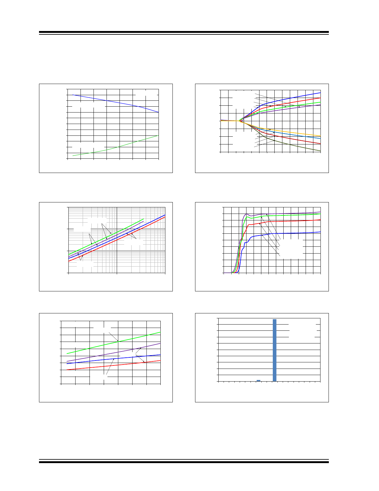
TYPICAL PERFORMANCE CURVES
Note:
Unless otherwise indicated, T
A
= +25°C, V
DD
= +2V to 5.5V, V
SS
= GND, V
CM
= V
DD
/3, V
OUT
= V
DD
/2,
V
L
= V
DD
/2, R
L
= 20 kΩ to V
L
and C
L
= 30 pF.
2.1
DC Input Precision
FIGURE 2-1:
Input Offset Voltage.
FIGURE 2-2:
Input Offset Voltage Drift.
FIGURE 2-3:
Input Offset Voltage
Quadratic Temp. Co.
FIGURE 2-4:
Input Offset Voltage vs.
Power Supply Voltage with V
CM
= V
CML
.
FIGURE 2-5:
Input Offset Voltage vs.
Power Supply Voltage with V
CM
= V
CMH
.
FIGURE 2-6:
Input Offset Voltage vs.
Output Voltage with V
DD
= 2.0V.
Note:
The graphs and tables provided following this note are a statistical summary based on a limited number of
samples and are provided for informational purposes only. The performance characteristics listed herein
are not tested or guaranteed. In some graphs or tables, the data presented may be outside the specified
operating range (e.g., outside specified power supply range) and therefore outside the warranted range.
0%
5%
10%
15%
20%
25%
30%
35%
40%
45%
50%
-2 -1.5 -1 -0.5 0 0.5 1 1.5 2 2.5 3 3.5 4
Percentage of
Occurences
Input Offset Voltage (µV)
28 Samples
T
A
= 25ºC
V
DD
= 2V
V
DD
= 5.5V
0%
10%
20%
30%
40%
50%
60%
-12 -10 -8 -6 -4 -2
0
2
4
6
8 10 12
Percentage of
Occurances
Input Offset Voltage Drift; TC
1
(nV/°C)
28 Samples
T
A
= -40°C to +125°C
V
DD
= 2V
V
DD
= 5.5V
0%
10%
20%
30%
40%
50%
60%
70%
80%
-200 -160 -120 -80
-40
0
40
80
120
Percentage of
Occurrences
Input Offset Voltage Quadratric Temp Co;
TC
2
(pV/°C
2
)
28 Samples
T
A
= -40°C to +125°C
V
DD
= 2V
V
DD
= 5.5V
-8
-6
-4
-2
0
2
4
6
8
0.0
0.5
1.0
1.5
2.0
2.5
3.0
3.5
4.0
4.5
5.0
5.5
6.0
6.5
Input Offset V
o
ltage
(µV)
Power Supply Voltage (V)
Representative Part
V
CM
= V
CML
T
A
= +125°C
T
A
= +85°C
T
A
= +25°C
T
A
= - 40°C
-8
-6
-4
-2
0
2
4
6
8
0.0
0.5
1.0
1.5
2.0
2.5
3.0
3.5
4.0
4.5
5.0
5.5
6.0
6.5
Input Offset V
o
ltage
(µV)
Power Supply Voltage (V)
Representative Part
V
CM
= V
CMH
T
A
= - 40°C
T
A
= +25°C
T
A
= +85°C
T
A
= +125°C
-8
-6
-4
-2
0
2
4
6
8
0.0
0.2
0.4
0.6
0.8
1.0
1.2
1.4
1.6
1.8
2.0
Input Offset V
o
ltage
(µV)
Output Voltage (V)
Representative Part
V
DD
= 2.0V
T
A
= +125°C
T
A
= +85°C
T
A
= +25°C
T
A
= -40°C
MCP6V71/1U/2/4
DS20005385B-page 8
2015 Microchip Technology Inc.
Note:
Unless otherwise indicated, T
A
= +25°C, V
DD
= +2V to 5.5V, V
SS
= GND, V
CM
= V
DD
/3, V
OUT
= V
DD
/2,
V
L
= V
DD
/2, R
L
= 20 kΩ to V
L
and C
L
= 30 pF.
FIGURE 2-7:
Input Offset Voltage vs.
Output Voltage with V
DD
= 5.5V.
FIGURE 2-8:
Input Offset Voltage vs.
Common Mode Voltage with V
DD
= 2V.
FIGURE 2-9:
Input Offset Voltage vs.
Common Mode Voltage with V
DD
= 5.5V.
FIGURE 2-10:
Common Mode Rejection
Ratio.
FIGURE 2-11:
Power Supply Rejection
Ratio.
FIGURE 2-12:
DC Open-Loop Gain.
-8
-6
-4
-2
0
2
4
6
8
0.0 0.5 1.0 1.5 2.0 2.5 3.0 3.5 4.0 4.5 5.0 5.5
Input Offset V
o
ltage
(µV)
Power Supply Voltage (V)
Representative Part
V
DD
= 5.5V
T
A
= - 40°C
T
A
= +25°C
T
A
= +85°C
T
A
= +125°C
-8
-6
-4
-2
0
2
4
6
8
-0.5
0.0
0.5
1.0
1.5
2.0
2.5
Input Offset V
o
ltage
(µV)
Common Mode Input Voltage (V)
Representative Part
V
DD
= 2.0V
T
A
= +125°C
T
A
= +85°C
T
A
= +25°C
T
A
= - 40°C
-8
-6
-4
-2
0
2
4
6
8
-0.5
0.0
0.5
1.0
1.5
2.0
2.5
3.0
3.5
4.0
4.5
5.0
5.5
6.0
Input Offset V
o
ltage
(µV)
Common Mode Input Voltage (V)
Representative Part
V
DD
= 5.5V
T
A
= +125°C
T
A
= +85°C
T
A
= +25°C
T
A
= -40°C
0%
5%
10%
15%
20%
25%
30%
35%
40%
45%
50%
-1.6
-1.2
-0.8
-0.4
0
0.4
0.8
1.2
1.6
Percentage of
Occurrences
1/CMRR (µV/V)
617 Samples
T
A
= +25ºC
V
DD
= 2V
V
DD
= 5.5V
Tester Data
0%
10%
20%
30%
40%
50%
60%
-1 -0.8 -0.6 -0.4 -0.2
0
0.2 0.4 0.6 0.8
1
Percentage of
Occurrences
1/PSRR (µV/V)
Tester Data
617 Samples
T
A
= +25ºC
0%
10%
20%
30%
40%
50%
60%
70%
-0.5 -0.4 -0.3 -0.2 -0.1 0
0.1 0.2 0.3 0.4 0.5
Percentage of
Occurrences
1/A
OL
(µV/V)
Tester Data
617 Samples
T
A
= +25ºC
V
DD
= 5.5V
V
DD
= 2.0V
2015 Microchip Technology Inc.
DS20005385B-page 9
MCP6V71/1U/2/4
Note:
Unless otherwise indicated, T
A
= +25°C, V
DD
= +2V to 5.5V, V
SS
= GND, V
CM
= V
DD
/3, V
OUT
= V
DD
/2,
V
L
= V
DD
/2, R
L
= 20 kΩ to V
L
and C
L
= 30 pF.
FIGURE 2-13:
CMRR and PSRR vs.
Ambient Temperature.
FIGURE 2-14:
DC Open-Loop Gain vs.
Ambient Temperature.
FIGURE 2-15:
Input Bias and Offset
Currents vs. Common Mode Input Voltage with
T
A
= +85°C.
FIGURE 2-16:
Input Bias and Offset
Currents vs. Common Mode Input Voltage with
T
A
= +125°C.
FIGURE 2-17:
Input Bias and Offset
Currents vs. Ambient Temperature with
V
DD
= +5.5V.
FIGURE 2-18:
Input Bias Current vs. Input
Voltage (below V
SS
).
110
120
130
140
150
160
-50
-25
0
25
50
75
100
125
CMRR, PSRR (dB)
Ambient Temperature (°C)
PSRR
CMRR @ V
DD
= 5.5V
@ V
DD
= 2V
110
120
130
140
150
160
170
-50
-25
0
25
50
75
100
125
DC Open-Loop Gain (dB)
Ambient Temperature (°C)
V
DD
= 5.5V
V
DD
= 2V
-1,000
-800
-600
-400
-200
0
200
400
600
800
1,000
-0.5
0.0
0.5
1.0
1.5
2.0
2.5
3.0
3.5
4.0
4.5
5.0
5.5
6.0
Input Bias and
Offset Currents
(pA)
Input Common Mode Voltage (V)
Input Bias Current
Input Offset Current
V
DD
= 5.5 V
T
A
= 85ºC
-1000
-800
-600
-400
-200
0
200
400
600
800
1000
-0.5
0.0
0.5
1.0
1.5
2.0
2.5
3.0
3.5
4.0
4.5
5.0
5.5
6.0
Input Bias and
Offset Currents
(pA)
Input Common Mode Voltage (V)
Input Bias Current
Input Offset Current
V
DD
= 5.5 V
T
A
= 125ºC
0.1
1
10
100
1000
25
35
45
55
65
75
85
95
105
115
125
Input Bias, Offset
Currents (A)
Ambient Temperature (°C)
Input Bias Current
Input Offset Current
V
DD
= 5.5 V
1n
100p
10p
1p
0.1p
-1.0 -0.9 -0.8 -0.7 -0.6 -0.5 -0.4 -0.3 -0.2 -0.1 0.0
Input Current Magnitude (A)
Input Voltage (V)
T
A
= +125°C
T
A
= +85°C
T
A
= +25°C
T
A
= -40°C
1m
10µ
100n
10n
1n
100µ
1µ
100p
MCP6V71/1U/2/4
DS20005385B-page 10
2015 Microchip Technology Inc.
Note:
Unless otherwise indicated, T
A
= +25°C, V
DD
= +2V to 5.5V, V
SS
= GND, V
CM
= V
DD
/3, V
OUT
= V
DD
/2,
V
L
= V
DD
/2, R
L
= 20 kΩ to V
L
and C
L
= 30 pF.
2.2
Other DC Voltages and Currents
FIGURE 2-19:
Input Common Mode
Voltage Headroom (Range) vs. Ambient
Temperature.
FIGURE 2-20:
Output Voltage Headroom
vs. Output Current.
FIGURE 2-21:
Output Voltage Headroom
vs. Ambient Temperature.
FIGURE 2-22:
Output Short Circuit Current
vs. Power Supply Voltage.
FIGURE 2-23:
Supply Current vs. Power
Supply Voltage.
FIGURE 2-24:
Power-On Reset Trip
Voltage.
-0.5
-0.4
-0.3
-0.2
-0.1
0.0
0.1
0.2
0.3
0.4
0.5
0.6
0.7
-50
-25
0
25
50
75
100
125
Input Common Mode V
o
ltage
Headroom (V)
Ambient Temperature (°C)
1 Wafer Lot
Upper (V
CMH
– V
DD
)
Lower (V
CML
– V
SS
)
1
10
100
1000
0.1
1
10
Output V
o
ltage Headroom
(mV)
Output Current Magnitude (mA)
V
DD
= 5.5V
V
DD
= 2V
V
DD
-V
OH
V
OL
-V
SS
0
10
20
30
40
50
60
70
80
90
-50
-25
0
25
50
75
100
125
Output V
oltage Headroom
(mV)
Ambient Temperature (°C)
V
DD
- V
OH
V
DD
= 5.5V
V
DD
- V
OH
V
OL
- V
SS
V
DD
= 2V
R
L
= 2 k
Ω
-40
-30
-20
-10
0
10
20
30
40
0 0.5 1 1.5 2 2.5 3 3.5 4 4.5 5 5.5 6 6.5
Output Short Circuit Current
(mA)
Power Supply Voltage (V)
T
A
= +125°C
T
A
= +85°C
T
A
= +25°C
T
A
= -40°C
T
A
= +125°C
T
A
= +85°C
T
A
= +25°C
T
A
= -40°C
0
20
40
60
80
100
120
140
160
180
200
0 0.5 1 1.5 2 2.5 3 3.5 4 4.5 5 5.5 6 6.5
Quiescent Current
(µA/Amplifier)
Power Supply Voltage (V)
T
A
= +125°C
T
A
= +85°C
T
A
= +25°C
T
A
= -40°C
0%
10%
20%
30%
40%
50%
60%
70%
80%
90%
100%
0.9
1.04
1.08
1.12
1.16
1.2
1.24
1.28
1.32
1.6
Percentage of
Occurences
POR Trip Voltage (V)
800 Samples
1 Wafer Lot
T
A
= +25ºC