
2012-2014 Microchip Technology Inc.
DS20002325C-page 1
MCP6H71/2/4
Features:
• Input Offset Voltage: ±1 mV (typical)
• Quiescent Current:
480 µA (typical)
• Common Mode Rejection Ratio: 103 dB (typical)
• Power Supply Rejection Ratio: 105 dB (typical)
• Rail-to-Rail Output
• Supply Voltage Range:
- Single-Supply Operation: 3.5V to 12V
- Dual-Supply Operation: ±1.75V to ±6V
• Gain Bandwidth Product: 2.7 MHz (typical)
• Slew Rate: 2 V/µs (typical)
• Unity Gain Stable
• Extended Temperature Range: -40°C to +125°C
• No Phase Reversal
Applications:
• Automotive Power Electronics
• Industrial Control Equipment
• Battery Powered Systems
• Sensor Conditioning
Design Aids:
• SPICE Macro Models
• FilterLab
®
Software
• MAPS (Microchip Advanced Part Selector)
• Analog Demonstration and Evaluation Boards
• Application Notes
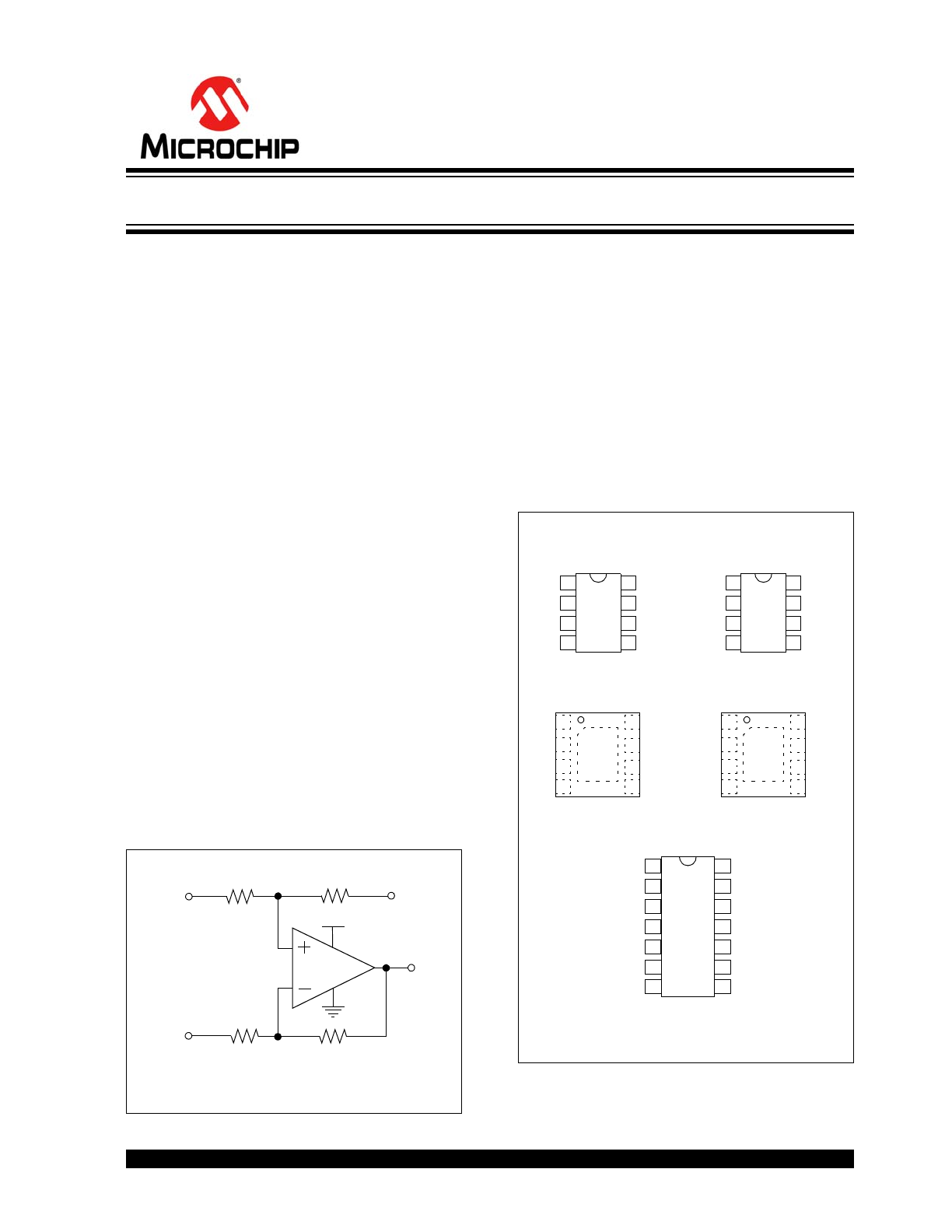
Typical Application
Description:
Microchip’s MCP6H71/2/4 family of operational
amplifiers (op amps) has a wide supply voltage range
of 3.5V to 12V and rail-to-rail output operation. This
family is unity gain stable and has a gain bandwidth
product of 2.7 MHz (typical). These devices operate
with a single-supply voltage as high as 12V, while only
drawing 480 µA/amplifier (typical) of quiescent current.
The MCP6H71/2/4 family is offered in single
(MCP6H71), dual (MCP6H72) and quad (MCP6H74)
configurations. All devices are fully specified in
extended temperature range from -40°C to +125°C.
Package Types
Difference Amplifier
R
1
V
OUT
R
2
R
1
V
REF
R
2
V
DD
V
1
V
2
MCP6H71
* Includes Exposed Thermal Pad (EP); see
Table 3-1
.
1
2
3
4
8
7
6
5
EP
9
V
DD
V
OUT
NC
NC
V
IN
+
V
IN
–
V
SS
NC
1
2
3
4
8
7
6
5
EP
9
V
OUTB
V
INB
–
V
INB
+
V
DD
V
INA
+
V
INA
–
V
SS
V
OUTA
V
INA
+
V
INA
–
V
SS
1
2
3
4
8
7
6
5
V
OUTA
V
DD
V
OUTB
V
INB
–
V
INB
+
V
IN
+
V
IN
–
V
SS
1
2
3
4
8
7
6
5
NC
NC
V
DD
V
OUT
NC
MCP6H71
SOIC
MCP6H72
SOIC
MCP6H71
2x3 TDFN
MCP6H72
2x3 TDFN
MCP6H74
SOIC, TSSOP
V
INA
+
V
INA
–
V
DD
1
2
3
4
14
13
12
11
V
OUTA
V
OUTD
V
IND
–
V
IND
+
V
SS
V
INB
+ 5
10 V
INC
+
V
INB
– 6
9
V
OUTB
7
8 V
OUTC
V
INC
–
2.7 MHz, 12V Op Amps

MCP6H71/2/4
DS20002325C-page 2
2012-2014 Microchip Technology Inc.
NOTES:
2012-2014 Microchip Technology Inc.
DS20002325C-page 3
MCP6H71/2/4
1.0
ELECTRICAL
CHARACTERISTICS
1.1
Absolute Maximum Ratings †
V
DD
– V
SS
.......................................................................13.2V
Current at Input Pins......................................................±2 mA
Analog Inputs (V
IN
+, V
IN
-)††.............V
SS
– 1.0V to V
DD
+ 1.0V
All Other Inputs and Outputs ............V
SS
– 0.3V to V
DD
+ 0.3V
Difference Input Voltage..........................................V
DD
– V
SS
Output Short-Circuit Current...................................continuous
Current at Output and Supply Pins ..............................±65 mA
Storage Temperature.....................................-65°C to +150°C
Maximum Junction Temperature (T
J
)...........................+150°C
ESD protection on all pins (HBM; MM)
2 kV; 200V
† Notice: Stresses above those listed under “Absolute
Maximum Ratings” may cause permanent damage to
the device. This is a stress rating only and functional
operation of the device at those or any other conditions
above those indicated in the operational listings of this
specification is not implied. Exposure to maximum
rating conditions for extended periods may affect
device reliability.
†† See
Section 4.1.2, Input Voltage Limits
.
DC ELECTRICAL SPECIFICATIONS
Electrical Characteristics: Unless otherwise indicated, V
DD
= +3.5V to +12V, V
SS
= GND, T
A
= +25°C,
V
CM
= V
DD
/2 - 1.4V, V
OUT
V
DD
/2, V
L
= V
DD
/2 and R
L
= 10 k
to V
L
. (Refer to
Figure 1-1
).
Parameters
Sym.
Min.
Typ.
Max.
Units
Conditions
Input Offset
Input Offset Voltage
V
OS
-4
±1
4
mV
Input Offset Drift with Temperature
V
OS
/
T
A
—
±2.5
—
µV/°C T
A
= -40°C to +125°C
Power Supply Rejection Ratio
PSRR
82
105
—
dB
Input Bias Current and Impedance
Input Bias Current
I
B
—
10
—
pA
—
400
—
pA
T
A
= +85°C
—
9
25
nA
T
A
= +125°C
Input Offset Current
I
OS
—
±1
—
pA
Common Mode Input Impedance
Z
CM
—
10
13
||6
—
||pF
Differential Input Impedance
Z
DIFF
—
10
13
||6
—
||pF
Common Mode
Common Mode Input Voltage Range
V
CMR
V
SS
– 0.3
—
V
DD
– 2.5
V
Common Mode Rejection Ratio
CMRR
76
96
—
dB
V
CM
= -0.3V to 1.0V,
V
DD
= 3.5V
80
99
—
dB
V
CM
= -0.3V to 2.5V,
V
DD
= 5V
80
103
—
dB
V
CM
= -0.3V to 9.5V,
V
DD
= 12V
Open-Loop Gain
DC Open-Loop Gain (Large Signal)
A
OL
100
120
—
dB
0.2V < V
OUT
<(V
DD
–
0.2V)
MCP6H71/2/4
DS20002325C-page 4
2012-2014 Microchip Technology Inc.
Output
High-Level Output Voltage
V
OH
3.490
3.495
—
V
V
DD
= 3.5V
0.5V input overdrive
4.985
4.993
—
V
V
DD
= 5V
0.5V input overdrive
11.970
11.980
—
V
V
DD
= 12V
0.5V input overdrive
Low-Level Output Voltage
V
OL
—
0.005
0.010
V
V
DD
= 3.5V
0.5 V input overdrive
—
0.007
0.015
V
V
DD
= 5V
0.5 V input overdrive
—
0.020
0.030
V
V
DD
= 12V
0.5 V input overdrive
Output Short-Circuit Current
I
SC
—
±32
—
mA
V
DD
= 3.5V
—
±50
—
mA
V
DD
= 5V
—
±53
—
mA
V
DD
= 12V
Power Supply
Supply Voltage
V
DD
3.5
—
12
V
Single-Supply operation
±1.75
—
±6
V
Dual-Supply operation
Quiescent Current per Amplifier
I
Q
—
480
600
µA
I
O
= 0, V
CM
= V
DD
/4
AC ELECTRICAL SPECIFICATIONS
Electrical Characteristics: Unless otherwise indicated, T
A
= +25°C, V
DD
= +3.5V to +12V, V
SS
= GND,
V
CM
= V
DD
/2 - 1.4V, V
OUT
V
DD
/2, V
L
= V
DD
/2, R
L
= 10 k
to V
L
and C
L
= 60 pF. (Refer to
Figure 1-1
).
Parameters
Sym.
Min.
Typ.
Max.
Units
Conditions
AC Response
Gain Bandwidth Product
GBWP
—
2.7
—
MHz
Phase Margin
PM
—
57
—
°C
G = +1V/V
Slew Rate
SR
—
2
—
V/µs
Noise
Input Noise Voltage
E
ni
—
11
—
µVp-p
f = 0.1 Hz to 10 Hz
Input Noise Voltage Density
E
ni
—
28
—
nV/
Hz f = 1 kHz
—
16
—
nV/
Hz f = 10 kHz
Input Noise Current Density
i
ni
—
1.9
—
fA/
Hz
f = 1 kHz
DC ELECTRICAL SPECIFICATIONS (CONTINUED)
Electrical Characteristics: Unless otherwise indicated, V
DD
= +3.5V to +12V, V
SS
= GND, T
A
= +25°C,
V
CM
= V
DD
/2 - 1.4V, V
OUT
V
DD
/2, V
L
= V
DD
/2 and R
L
= 10 k
to V
L
. (Refer to
Figure 1-1
).
Parameters
Sym.
Min.
Typ.
Max.
Units
Conditions
2012-2014 Microchip Technology Inc.
DS20002325C-page 5
MCP6H71/2/4
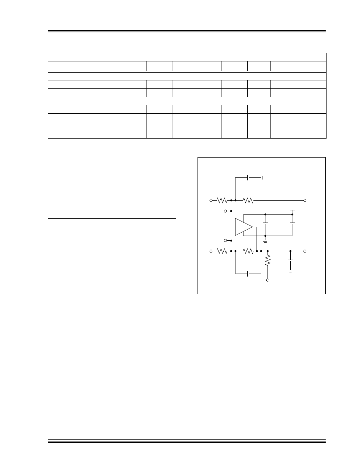
1.2
Test Circuits
The circuit used for most DC and AC tests is shown in
Figure 1-1
. This circuit can independently set V
CM
and
V
OUT
(refer to
Equation 1-1
). Note that V
CM
is not the
circuit’s common mode voltage ((V
P
+ V
M
)/2), and that
V
OST
includes V
OS
plus the effects (on the input offset
error, V
OST
) of temperature, CMRR, PSRR and A
OL
.
EQUATION 1-1:
FIGURE 1-1:
AC and DC Test Circuit for
Most Specifications.
TEMPERATURE SPECIFICATIONS
Electrical Characteristics: Unless otherwise indicated, V
DD
= +3.5V to +12V and V
SS
= GND.
Parameters
Sym.
Min.
Typ.
Max.
Units
Conditions
Temperature Ranges
Operating Temperature Range
T
A
-40
—
+125
°C
Note 1
Storage Temperature Range
T
A
-65
—
+150
°C
Thermal Package Resistances
Thermal Resistance, 8L-SOIC
JA
—
149.5
—
°C/W
Thermal Resistance, 8L-2x3 TDFN
JA
—
52.5
—
°C/W
Thermal Resistance, 14L-SOIC
JA
—
95.3
—
°C/W
Thermal Resistance, 14L-TSSOP
JA
—
100
—
°C/W
Note 1: The internal junction temperature (T
J
) must not exceed the absolute maximum specification of +150°C.
G
DM
R
F
R
G
=
V
CM
V
P
V
DD
2
+
2
=
V
OUT
V
DD
2
V
P
V
M
–
V
OST
1
G
DM
+
+
+
=
Where:
G
DM
= Differential Mode Gain
(V/V)
V
CM
= Op Amp’s Common Mode
Input Voltage
(V)
V
OST
= Op Amp’s Total Input Offset
Voltage
(mV)
V
OST
V
IN –
V
IN+
–
=
V
DD
R
G
R
F
V
OUT
V
M
C
B2
C
L
R
L
V
L
C
B1
100 k
100 k
R
G
R
F
V
DD
/2
V
P
100 k
100 k
60 pF
10 k
1 µF
100 nF
V
IN–
V
IN+
C
F
6.8 pF
C
F
6.8 pF
MCP6H7X

MCP6H71/2/4
DS20002325C-page 6
2012-2014 Microchip Technology Inc.
NOTES:
2012-2014 Microchip Technology Inc.
DS20002325C-page 7
MCP6H71/2/4
2.0
TYPICAL PERFORMANCE CURVES
Note: Unless otherwise indicated, T
A
= +25°C, V
DD
= +3.5V to +12V, V
SS
= GND, V
CM
= V
DD
/2 - 1.4V, V
OUT
V
DD
/2,
V
L
= V
DD
/2, R
L
= 10 k
to V
L
and C
L
= 60 pF.
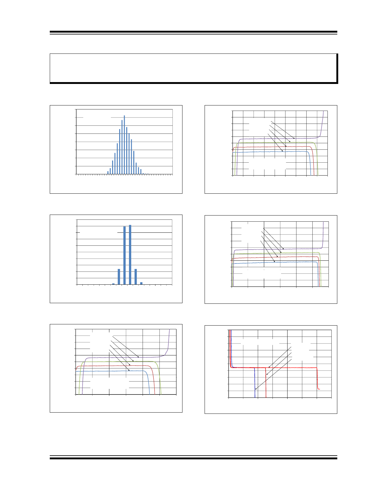
FIGURE 2-1:
Input Offset Voltage.
FIGURE 2-2:
Input Offset Voltage Drift.
FIGURE 2-3:
Input Offset Voltage vs.
Common Mode Input Voltage.
FIGURE 2-4:
Input Offset Voltage vs.
Common Mode Input Voltage.
FIGURE 2-5:
Input Offset Voltage vs.
Common Mode Input Voltage.
FIGURE 2-6:
Input Offset Voltage vs.
Output Voltage.
Note:
The graphs and tables provided following this note are a statistical summary based on a limited number of
samples and are provided for informational purposes only. The performance characteristics listed herein
are not tested or guaranteed. In some graphs or tables, the data presented may be outside the specified
operating range (e.g., outside specified power supply range) and therefore outside the warranted range.
6%
8%
10%
12%
14%
16%
n
tage of Occurances
800 Samples
0%
2%
4%
-4.0
-3.0
-2.0
-1.0
0.0
1.0
2.0
3.0
4.0
Perce
n
Input Offset Voltage (mV)
15%
20%
25%
30%
35%
40%
45%
50%
tage of Occurances
800 Samples
T
A
= - 40°C to +125°C
0%
5%
10%
15%
-24
-21
-18
-15
-12
-9
-6
-3
0
3
6
9
12
15
18
21
24
Percen
Input Offset Voltage Drift (µV/°C)
-400
-200
0
200
400
600
800
1000
t Offset V
o
ltage
(µV)
T
A
= +125°C
T
A
= +85°C
T
A
= +25°C
T
A
= -40°C
-1000
-800
-600
-0.5
0.0
0.5
1.0
1.5
2.0
2.5
Inpu
t
Common Mode Input Voltage (V)
V
DD
= 3.5V
Representative Part
-400
-200
0
200
400
600
800
1000
t Offset V
o
ltage
(µV)
T
A
= +125°C
T
A
= +85°C
T
A
= +25°C
T
A
= -40°C
-1000
-800
-600
-0.5 0.0
0.5
1.0
1.5
2.0
2.5
3.0
3.5
4.0
Inpu
t
Common Mode Input Voltage (V)
V
DD
= 5V
Representative Part
-400
-200
0
200
400
600
800
1000
t Offset V
o
ltage
(µV)
T
A
= +125°C
T
A
= +85°C
T
A
= +25°C
T
A
= -40°C
V
= 12V
-1000
-800
-600
-0.5
1.5
3.5
5.5
7.5
9.5
11.5
Inpu
t
Common Mode Input Voltage (V)
V
DD
= 12V
Representative Part
-400
-200
0
200
400
600
800
1000
t Offset V
o
ltage
(µV)
V
DD
= 12V
V
DD
= 3.5V
Representative Part
V
DD
= 5V
-1000
-800
-600
0
2
4
6
8
10
12
14
Inpu
t
Output Voltage (V)
MCP6H71/2/4
DS20002325C-page 8
2012-2014 Microchip Technology Inc.
Note: Unless otherwise indicated, T
A
= +25°C, V
DD
= +3.5V to +12V, V
SS
= GND, V
CM
= V
DD
/2 - 1.4V, V
OUT
V
DD
/2,
V
L
= V
DD
/2, R
L
= 10 k
to V
L
and C
L
= 60 pF.
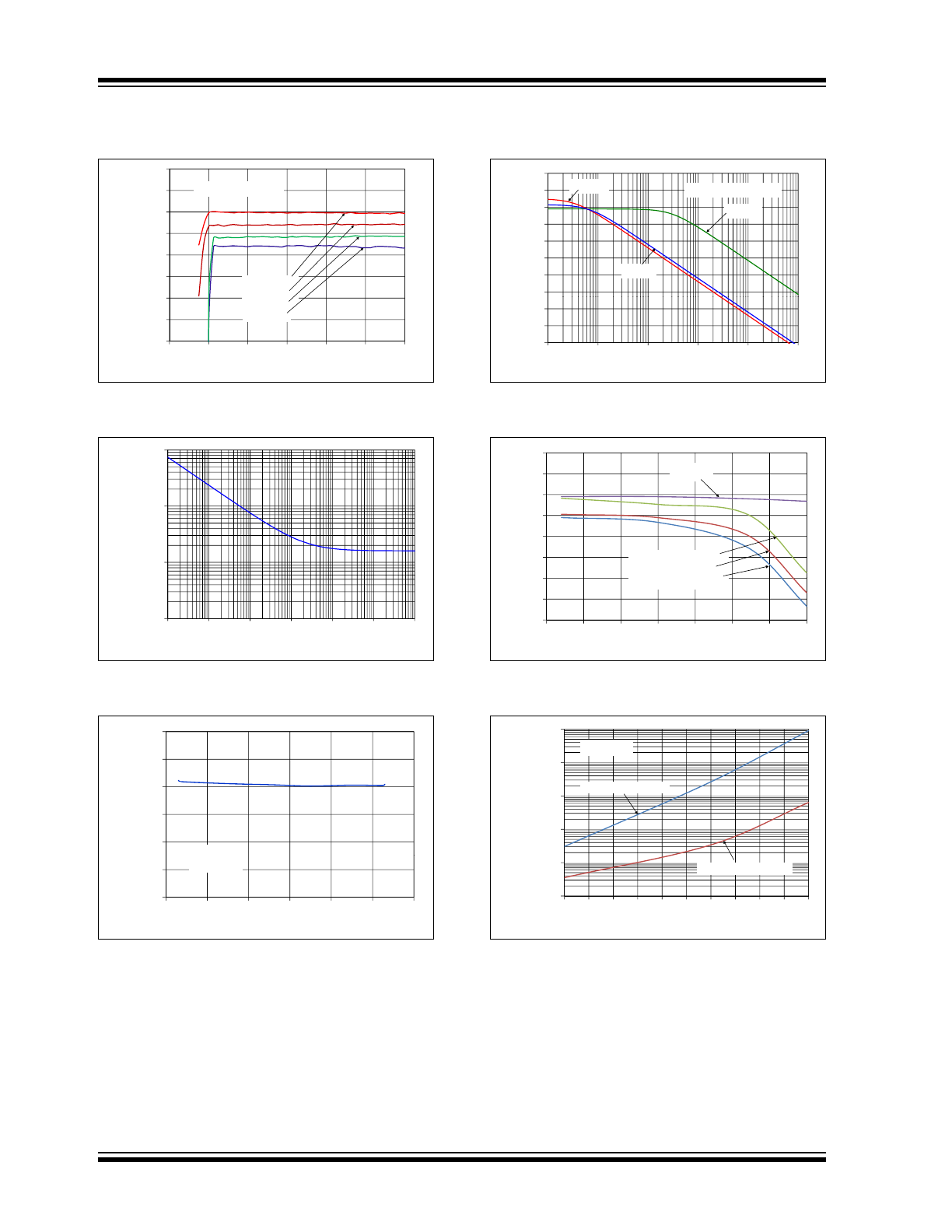
FIGURE 2-7:
Input Offset Voltage vs.
Power Supply Voltage.
FIGURE 2-8:
Input Noise Voltage Density
vs. Frequency.
FIGURE 2-9:
Input Noise Voltage Density
vs. Common Mode Input Voltage.
FIGURE 2-10:
CMRR, PSRR vs.
Frequency.
FIGURE 2-11:
CMRR, PSRR vs. Ambient
Temperature.
FIGURE 2-12:
Input Bias, Offset Currents
vs. Ambient Temperature.
-300
-200
-100
0
100
200
O
ffset V
o
ltage (uV)
T
A
= +125°C
Representative Part
-600
-500
-400
0
2
4
6
8
10
12
Input
O
Power Supply Voltage (V)
T
A
125 C
T
A
= +85°C
T
A
= +25°C
T
A
= -40°C
10
100
1,000
N
oise V
o
ltage Density
(nV/
¥
Hz)
1
1.E+0
1.E+1
1.E+2
1.E+3
1.E+4
1.E+5
1.E+6
Input
N
Frequency (Hz)
1 10 100
1k
10k 100k 1M
12
14
16
18
20
N
oise V
o
ltage Density
(nV/
¥
Hz)
f = 10 kHz
8
10
-1
1
3
5
7
9
11
Input
N
Common Mode Input Voltage (V)
f 10 kHz
V
DD
= 12 V
50
60
70
80
90
100
110
120
M
RR, PSRR
(dB)
CMRR
PSRR+
PSRR-
Representative Part
20
30
40
10
100
1000
10000
100000
1000000
C
M
Frequency (Hz)
10 100 1k
10k
100k 1M
70
80
90
100
110
120
130
C
MRR, PSRR
(dB)
PSRR
CMRR @ V
DD
= 12V
@ V
DD
= 5V
@ V
3 5V
50
60
70
-50
-25
0
25
50
75
100
125
C
Ambient Temperature (°C)
@ V
DD
= 3.5V
10
100
1000
10000
as and Offset
Currents
(A)
Input Bias Current
V
DD
= 12 V
10n
1n
100p
10p
0.1
1
25
35
45
55
65
75
85
95
105
11
5
125
Input Bi
Ambient Temperature (°C)
Input Offset Current
1p
0.1p
2012-2014 Microchip Technology Inc.
DS20002325C-page 9
MCP6H71/2/4
Note: Unless otherwise indicated, T
A
= +25°C, V
DD
= +3.5V to +12V, V
SS
= GND, V
CM
= V
DD
/2 - 1.4V, V
OUT
V
DD
/2,
V
L
= V
DD
/2, R
L
= 10 k
to V
L
and C
L
= 60 pF.
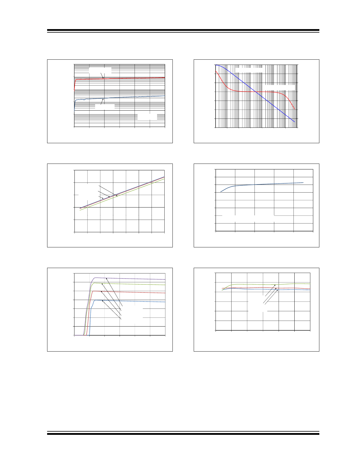
FIGURE 2-13:
Input Bias Current vs.
Common Mode Input Voltage.
FIGURE 2-14:
Quiescent Current vs.
Ambient Temperature.
FIGURE 2-15:
Quiescent Current vs.
Power Supply Voltage.
FIGURE 2-16:
Open-Loop Gain, Phase vs.
Frequency.
FIGURE 2-17:
DC Open-Loop Gain vs.
Power Supply Voltage.
FIGURE 2-18:
DC Open-Loop Gain vs.
Output Voltage Headroom.
100
1000
10000
100000
u
t
Bias Current (A)
T
A
= +125°C
T
A
= +85°C
100n
10n
1n
100p
1
10
0
2
4
6
8
10
12
Inp
u
Common Mode Input Voltage (V)
V
DD
= 12 V
10p
1p
400
500
600
700
u
iescent Current
(uA/Amplifier)
V
DD
= 12V
V
DD
= 5V
V
DD
= 3.5V
200
300
-50
-25
0
25
50
75
100
125
Q
u
Ambient Temperature (°C)
200
300
400
500
600
700
Q
uiescent Current
(uA/Amplifier)
T
A
= +125°C
T
A
= +85°C
T
A
= +25°C
T
40°C
0
100
0
2
4
6
8
10
12
Q
Power Supply Voltage (V)
T
A
= -40°C
-150
-120
-90
-60
-30
0
20
40
60
80
100
120
e
n-Loop Phase
(°)
e
n-Loop Gain (dB)
Open-Loop Gain
Open-Loop Phase
-210
-180
150
-20
0
20
1.0E+00
1.0E+01
1.0E+02
1.0E+03
1.0E+04
1.0E+05
1.0E+06
1.0E+07
Op
e
Op
e
Frequency (Hz)
1 10 100 1k 10k 100k 1M 10M
100
110
120
130
140
150
160
pen Loop Gain (dB)
80
90
100
3
5
7
9
11
13
DC-O
Power Supply Voltage (V)
V
SS
+ 0.2V < V
OUT
< V
DD
- 0.2V
80
100
120
140
160
-Open Loop Gain (dB)
V
DD
= 12V
V
DD
= 5V
V
DD
= 3.5V
40
60
0.00
0.05
0.10
0.15
0.20
0.25
0.30
DC
-
Output Voltage Headroom (V)
V
DD
- V
OH
or V
OL
- V
SS
MCP6H71/2/4
DS20002325C-page 10
2012-2014 Microchip Technology Inc.
Note: Unless otherwise indicated, T
A
= +25°C, V
DD
= +3.5V to +12V, V
SS
= GND, V
CM
= V
DD
/2 - 1.4V, V
OUT
V
DD
/2,
V
L
= V
DD
/2, R
L
= 10 k
to V
L
and C
L
= 60 pF.
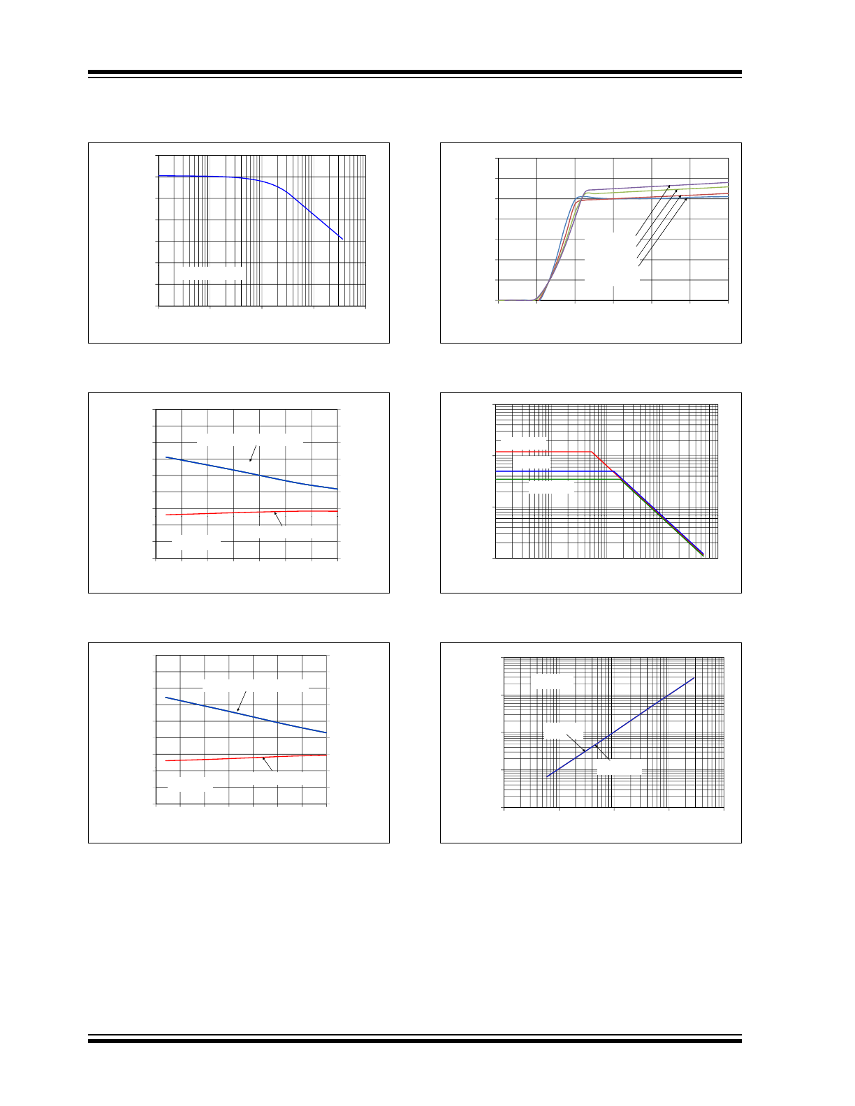
FIGURE 2-19:
Channel-to-Channel
Separation vs. Frequency (MCP6H72/4 only).
FIGURE 2-20:
Gain Bandwidth Product,
Phase Margin vs. Ambient Temperature.
FIGURE 2-21:
Gain Bandwidth Product,
Phase Margin vs. Ambient Temperature.
FIGURE 2-22:
Output Short Circuit Current
vs. Power Supply Voltage.
FIGURE 2-23:
Output Voltage Swing vs.
Frequency.
FIGURE 2-24:
Output Voltage Headroom
vs. Output Current.
90
100
110
120
130
140
h
annel to Channel
S
eparation (dB)
70
80
90
100
1000
10000
100000
100000
C
h
S
Frequency (Hz)
100 1k 10k
100k 1M
Input Referred
60
80
100
120
140
160
180
1.5
2.0
2.5
3.0
3.5
4.0
4.5
B
andw
idth Product
(MHz)
Gain Bandwidth Product
Gain Bandwidth Product
Gain Bandwidth Product
Gain Bandwidth Product
Gain Bandwidth Product
Gain Bandwidth Product
h
ase Mar
gin (°)
0
20
40
0.0
0.5
1.0
-50
-25
0
25
50
75
100 125
Gain
B
Ambient Temperature (°C)
Phase Margin
V
DD
= 3.5V
Phase Margin
V
DD
= 3.5V
Phase Margin
V
DD
= 3.5V
Phase Margin
V
DD
= 3.5V
Phase Margin
V
DD
= 3.5V
Phase Margin
V
DD
= 3.5V
P
h
40
60
80
100
120
140
160
180
1 0
1.5
2.0
2.5
3.0
3.5
4.0
4.5
n
Bandw
idth Product
(MHz)
Gain Bandwidth Product
P
hase Mar
gin (°)
0
20
40
0.0
0.5
1.0
-50
-25
0
25
50
75
100 125
Gai
n
Ambient Temperature (°C)
V
DD
= 12V
V
DD
= 12V
V
DD
= 12V
V
DD
= 12V
V
DD
= 12V
V
DD
= 12V
V
DD
= 12V
Phase Margin
V
DD
= 12V
P
20
30
40
50
60
70
t Short
Circuit Current
(mA)
T
A
= +125°C
T
A
= +85°C
T
A
= +25°C
T = 40°C
0
10
0
2
4
6
8
10
12
Outpu
Power Supply Voltage (V)
T
A
= -40 C
1
10
100
t V
o
ltage
Sw
ing (V
P-P
)
V
DD
= 3.5V
V
DD
= 5V
V
DD
= 12V
0.1
1000
10000
100000
1000000
10000000
Outpu
t
Frequency (Hz)
1k
10k 100k 1M 10M
1
10
100
1000
V
oltage Headroom (mV)
V
DD
- V
OH
V
OL
- V
SS
V
DD
= 12V
0.1
1
0.01
0.1
1
10
100
Output
V
Output Current (mA)
DD
OH