
2010-2011 Microchip Technology Inc.
DS22243D-page 1
MCP6H01/2/4
Features:
• Input Offset Voltage: ±0.7 mV (typical)
• Quiescent Current:
135 µA (typical)
• Common Mode Rejection Ratio: 100 dB (typical)
• Power Supply Rejection Ratio: 102 dB (typical)
• Rail-to-Rail Output
• Supply Voltage Range:
- Single-Supply Operation: 3.5V to 16V
- Dual-Supply Operation: ±1.75V to ±8V
• Gain Bandwidth Product: 1.2 MHz (typical)
• Slew Rate: 0.8V/µs (typical)
• Unity Gain Stable
• Extended Temperature Range: -40°C to +125°C
• No Phase Reversal
Applications:
• Automotive Power Electronics
• Industrial Control Equipment
• Battery Powered Systems
• Medical Diagnostic Instruments
Design Aids:
• SPICE Macro Models
• FilterLab
®
Software
• MAPS (Microchip Advanced Part Selector)
• Analog Demonstration and Evaluation Boards
• Application Notes
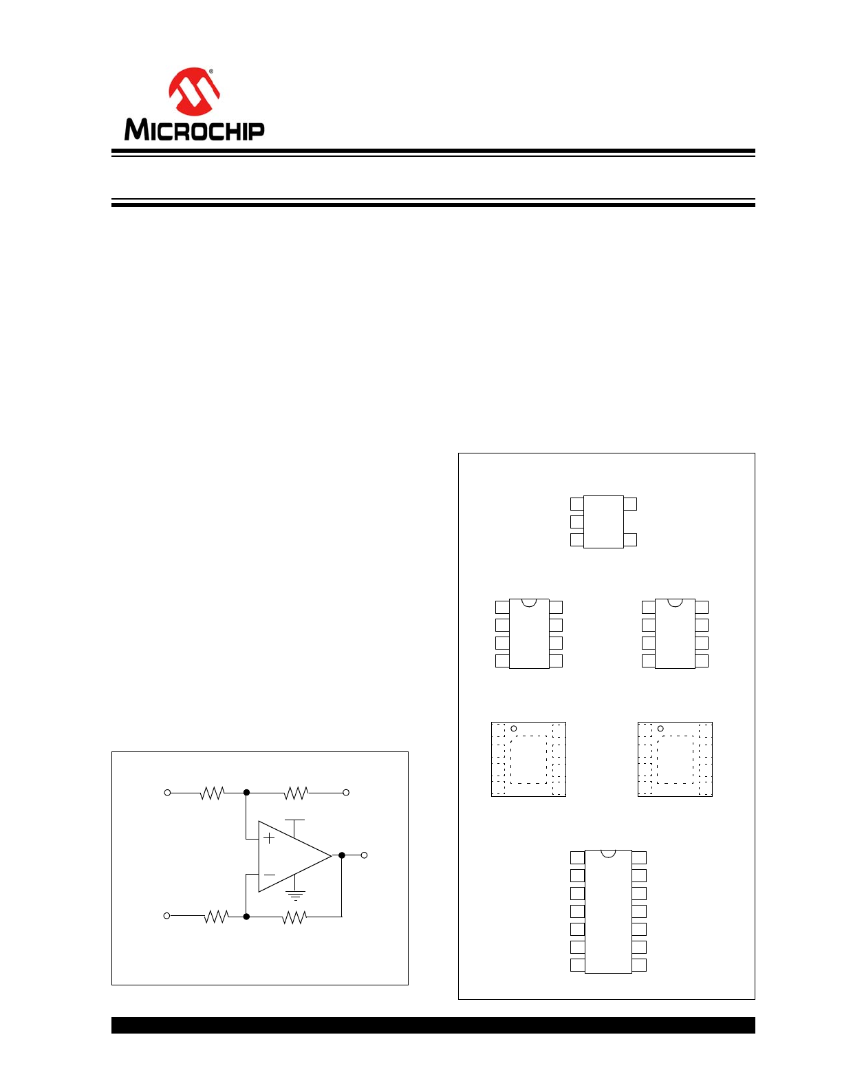
Typical Application
Description:
Microchip’s MCP6H01/2/4 family of operational amplifi-
ers (op amps) has a wide supply voltage range of 3.5V
to 16V and rail-to-rail output operation. This family is
unity gain stable and has a gain bandwidth product of
1.2 MHz (typical). These devices operate with a
single-supply voltage as high as 16V, while only
drawing 135 µA/amplifier (typical) of quiescent current.
The MCP6H01/2/4 family is offered in single
(MCP6H01), dual (MCP6H02) and quad (MCP6H04)
configurations. All devices are fully specified in
extended temperature range from -40°C to +125°C.
Package Types
Difference Amplifier
R
1
V
OUT
R
2
R
1
V
REF
R
2
V
DD
V
1
V
2
MCP6H01
* Includes Exposed Thermal Pad (EP); see
Table 3-1
.
1
2
3
4
8
7
6
5
EP
9
V
DD
V
OUT
NC
NC
V
IN
+
V
IN
–
V
SS
NC
1
2
3
4
8
7
6
5
EP
9
V
OUTB
V
INB
–
V
INB
+
V
DD
V
INA
+
V
INA
–
V
SS
V
OUTA
V
INA
+
V
INA
–
V
SS
1
2
3
4
8
7
6
5
V
OUTA
V
DD
V
OUTB
V
INB
–
V
INB
+
V
IN
+
V
IN
–
V
SS
1
2
3
4
8
7
6
5
NC
NC
V
DD
V
OUT
NC
MCP6H01
SOIC
MCP6H02
SOIC
MCP6H01
2x3 TDFN
MCP6H02
2x3 TDFN
MCP6H04
SOIC, TSSOP
V
INA
+
V
INA
–
V
DD
1
2
3
4
14
13
12
11
V
OUTA
V
OUTD
V
IND
–
V
IND
+
V
SS
V
INB
+ 5
10 V
INC
+
V
INB
– 6
9
V
OUTB
7
8 V
OUTC
V
INC
–
V
IN
+
V
IN
–
1
2
3
5
4
V
DD
V
OUT
MCP6H01
SC70-5, SOT 23-5
V
SS
1.2 MHz, 16V Op Amps

MCP6H01/2/4
DS22243D-page 2
2010-2011 Microchip Technology Inc.
NOTES:
2010-2011 Microchip Technology Inc.
DS22243D-page 3
MCP6H01/2/4
1.0
ELECTRICAL CHARACTERISTICS
1.1
Absolute Maximum Ratings †
V
DD
– V
SS
..........................................................................17V
Current at Input Pins......................................................±2 mA
Analog Inputs (V
IN
+, V
IN
-)††.............V
SS
– 1.0V to V
DD
+ 1.0V
All Other Inputs and Outputs ............V
SS
– 0.3V to V
DD
+ 0.3V
Difference Input Voltage..........................................V
DD
– V
SS
Output Short-Circuit Current...................................continuous
Current at Output and Supply Pins ..............................±65 mA
Storage Temperature.....................................-65°C to +150°C
Maximum Junction Temperature (T
J
)...........................+150°C
ESD protection on all pins (HBM; MM)
2 kV; 200V
† Notice: Stresses above those listed under “Absolute
Maximum Ratings” may cause permanent damage to the
device. This is a stress rating only and functional operation of
the device at those or any other conditions above those
indicated in the operational listings of this specification is not
implied. Exposure to maximum rating conditions for extended
periods may affect device reliability.
†† See
4.1.2 “Input Voltage Limits”
.
DC ELECTRICAL SPECIFICATIONS
Electrical Characteristics: Unless otherwise indicated, V
DD
= +3.5V to +16V, V
SS
= GND, T
A
= +25°C,
V
CM
= V
DD
/2 – 1.4V, V
OUT
V
DD
/2, V
L
= V
DD
/2 and R
L
= 10 k
to V
L
. (Refer to
Figure 1-1
).
Parameters
Sym
Min
Typ
Max
Units
Conditions
Input Offset
Input Offset Voltage
V
OS
-3.5
±0.7
+3.5
mV
Input Offset Drift with Temperature
V
OS
/
T
A
—
±2.5
—
µV/°C T
A
= -40°C to +125°C
Power Supply Rejection Ratio
PSRR
87
102
—
dB
Input Bias Current and Impedance
Input Bias Current
I
B
—
10
—
pA
I
B
—
600
—
pA
T
A
= +85°C
I
B
—
10
25
nA
T
A
= +125°C
Input Offset Current
I
OS
—
±1
—
pA
Common Mode Input Impedance
Z
CM
—
10
13
||6
—
||pF
Differential Input Impedance
Z
DIFF
—
10
13
||6
—
||pF
Common Mode
Common Mode Input Voltage Range
V
CMR
V
SS
0.3
—
V
DD
2.3
V
Common Mode Rejection Ratio
CMRR
78
93
—
dB
V
CM
= -0.3V to 1.2V,
V
DD
= 3.5V
82
98
—
dB
V
CM
= -0.3V to 2.7V,
V
DD
= 5V
84
100
—
dB
V
CM
= -0.3V to 12.7V,
V
DD
= 15V
Open-Loop Gain
DC Open-Loop Gain (Large Signal)
A
OL
95
115
—
dB
0.2V < V
OUT
<(V
DD
–
0.2V)
MCP6H01/2/4
DS22243D-page 4
2010-2011 Microchip Technology Inc.
AC ELECTRICAL SPECIFICATIONS
Output
High-Level Output Voltage
V
OH
3.490
3.495
—
V
V
DD
= 3.5V
0.5V input overdrive
4.985
4.993
—
V
V
DD
= 5V
0.5V input overdrive
14.970
14.980
—
V
V
DD
= 15V
0.5V input overdrive
Low-Level Output Voltage
V
OL
—
0.005
0.010
V
V
DD
= 3.5V
0.5 V input overdrive
—
0.007
0.015
V
V
DD
= 5V
0.5 V input overdrive
—
0.020
0.030
V
V
DD
= 15V
0.5 V input overdrive
Output Short-Circuit Current
I
SC
—
±27
—
mA
V
DD
= 3.5V
—
±45
—
mA
V
DD
= 5V
—
±50
—
mA
V
DD
= 15V
Power Supply
Supply Voltage
V
DD
3.5
—
16
V
Single-supply operation
±1.75
—
±8
V
Dual-supply operation
Quiescent Current per Amplifier
I
Q
—
125
175
µA
I
O
= 0, V
DD
= 3.5V
V
CM
= V
DD
/4
—
130
180
µA
I
O
= 0, V
DD
= 5V
V
CM
= V
DD
/4
—
135
185
µA
I
O
= 0, V
DD
= 15V
V
CM
= V
DD
/4
Electrical Characteristics: Unless otherwise indicated, T
A
= +25°C, V
DD
= +3.5V to +16V, V
SS
= GND,
V
CM
= V
DD
/2 - 1.4V, V
OUT
V
DD
/2, V
L
= V
DD
/2, R
L
= 10 k
to V
L
and C
L
= 60 pF. (Refer to
Figure 1-1
).
Parameters
Sym
Min
Typ
Max
Units
Conditions
AC Response
Gain Bandwidth Product
GBWP
—
1.2
—
MHz
Phase Margin
PM
—
57
—
°C
G = +1V/V
Slew Rate
SR
—
0.8
—
V/µs
Noise
Input Noise Voltage
E
ni
—
12
—
µVp-p
f = 0.1 Hz to 10 Hz
Input Noise Voltage Density
e
ni
—
35
—
nV/
Hz f = 1 kHz
—
30
—
nV/
Hz f = 10 kHz
Input Noise Current Density
i
ni
—
1.9
—
fA/
Hz f = 1 kHz
DC ELECTRICAL SPECIFICATIONS (CONTINUED)
Electrical Characteristics: Unless otherwise indicated, V
DD
= +3.5V to +16V, V
SS
= GND, T
A
= +25°C,
V
CM
= V
DD
/2 – 1.4V, V
OUT
V
DD
/2, V
L
= V
DD
/2 and R
L
= 10 k
to V
L
. (Refer to
Figure 1-1
).
Parameters
Sym
Min
Typ
Max
Units
Conditions
2010-2011 Microchip Technology Inc.
DS22243D-page 5
MCP6H01/2/4
TEMPERATURE SPECIFICATIONS
1.2
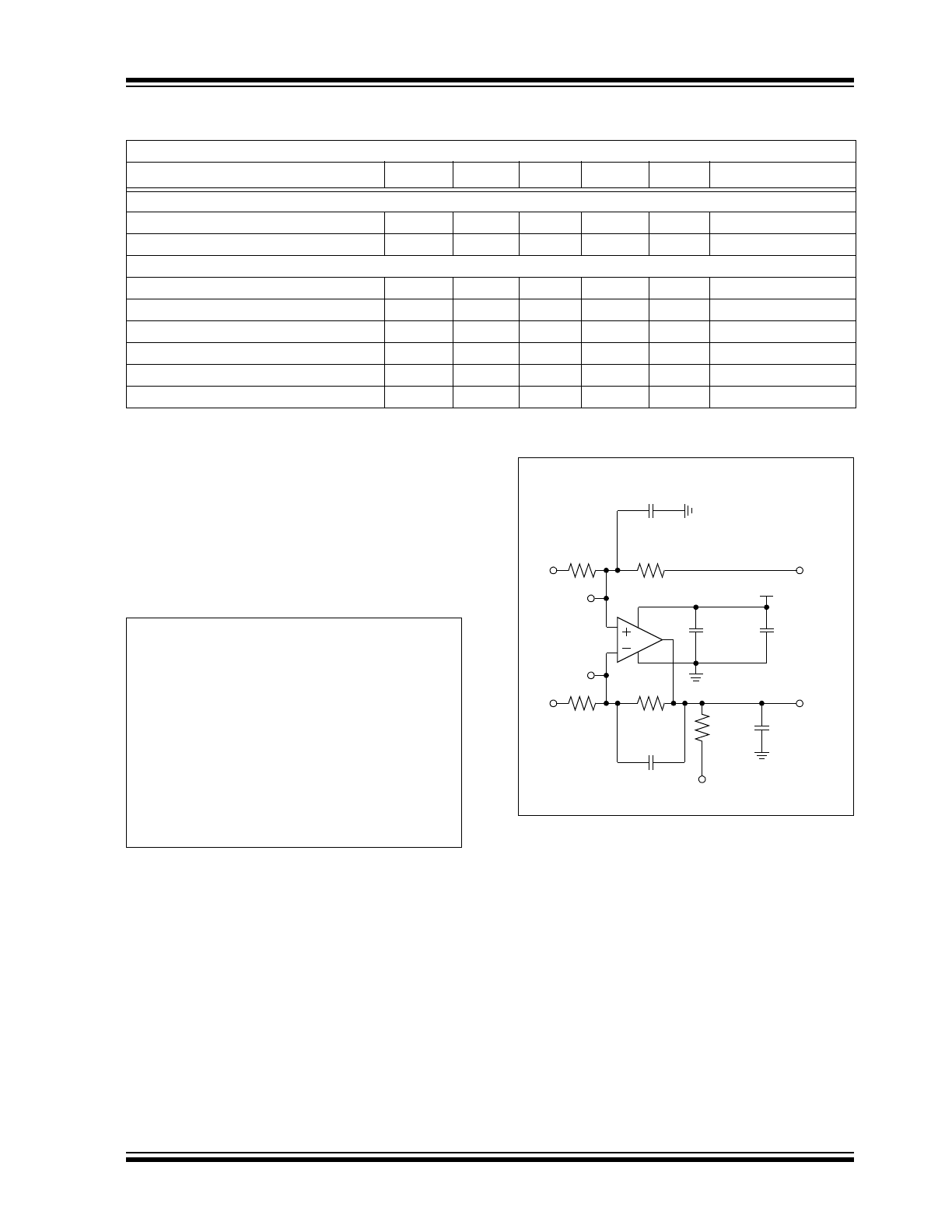
Test Circuits
The circuit used for most DC and AC tests is shown in
Figure 1-1
. This circuit can independently set V
CM
and
V
OUT
(refer to
Equation 1-1
). Note that V
CM
is not the
circuit’s common mode voltage ((V
P
+ V
M
)/2), and that
V
OST
includes V
OS
plus the effects (on the input offset
error, V
OST
) of temperature, CMRR, PSRR and A
OL
.
EQUATION 1-1:
FIGURE 1-1:
AC and DC Test Circuit for
Most Specifications.
Electrical Characteristics: Unless otherwise indicated, V
DD
= +3.5V to +16V and V
SS
= GND.
Parameters
Sym
Min
Typ
Max
Units
Conditions
Temperature Ranges
Operating Temperature Range
T
A
-40
—
+125
°C
Note 1
Storage Temperature Range
T
A
-65
—
+150
°C
Thermal Package Resistances
Thermal Resistance, 5L-SC70
JA
—
331
—
°C/W
Thermal Resistance, 5L-SOT-23
JA
—
256
—
°C/W
Thermal Resistance, 8L-2x3 TDFN
JA
—
41
—
°C/W
Thermal Resistance, 8L-SOIC
JA
—
149.5
—
°C/W
Thermal Resistance, 14L-SOIC
JA
—
95.3
—
°C/W
Thermal Resistance, 14L-TSSOP
JA
—
100
—
°C/W
Note 1: The internal junction temperature (T
J
) must not exceed the absolute maximum specification of +150°C.
G
DM
R
F
R
G
=
V
CM
V
P
V
DD
2
+
2
=
V
OUT
V
DD
2
V
P
V
M
–
V
OST
1
G
DM
+
+
+
=
Where:
G
DM
= Differential Mode Gain
(V/V)
V
CM
= Op Amp’s Common Mode
Input Voltage
(V)
V
OST
= Op Amp’s Total Input Offset
Voltage
(mV)
V
OST
V
IN –
V
IN+
–
=
V
DD
R
G
R
F
V
OUT
V
M
C
B2
C
L
R
L
V
L
C
B1
100 k
100 k
R
G
R
F
V
DD
/2
V
P
100 k
100 k
60 pF
10 k
1 µF
100 nF
V
IN–
V
IN+
C
F
6.8 pF
C
F
6.8 pF
MCP6H0X

MCP6H01/2/4
DS22243D-page 6
2010-2011 Microchip Technology Inc.
NOTES:
2010-2011 Microchip Technology Inc.
DS22243D-page 7
MCP6H01/2/4
2.0
TYPICAL PERFORMANCE CURVES
Note: Unless otherwise indicated, T
A
= +25°C, V
DD
= +3.5V to +16V, V
SS
= GND, V
CM
= V
DD
/2 - 1.4V, V
OUT
V
DD
/2,
V
L
= V
DD
/2, R
L
= 10 k
to V
L
and C
L
= 60 pF.
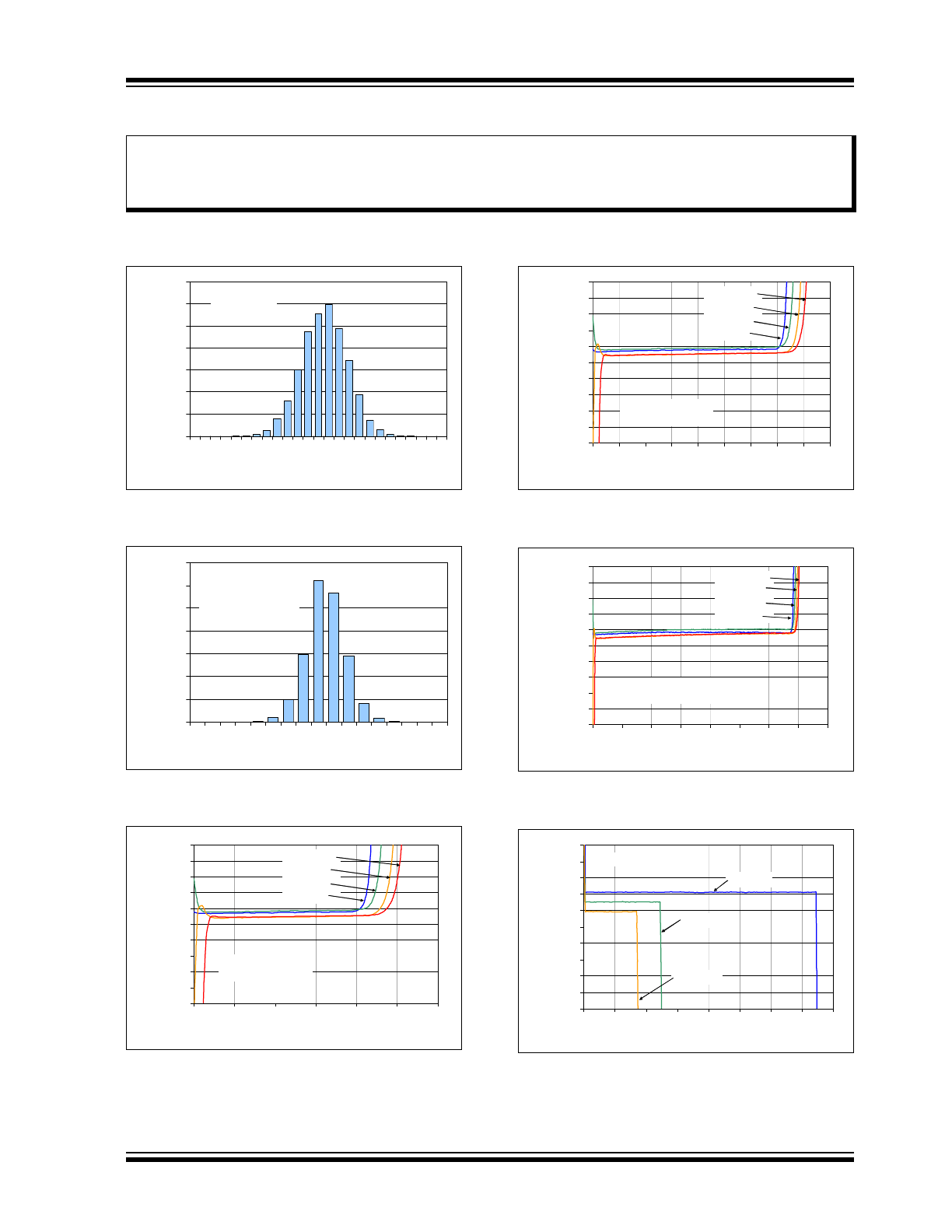
FIGURE 2-1:
Input Offset Voltage.
FIGURE 2-2:
Input Offset Voltage Drift.
FIGURE 2-3:
Input Offset Voltage vs.
Common Mode Input Voltage.
FIGURE 2-4:
Input Offset Voltage vs.
Common Mode Input Voltage.
FIGURE 2-5:
Input Offset Voltage vs.
Common Mode Input Voltage.
FIGURE 2-6:
Input Offset Voltage vs.
Output Voltage.
Note:
The graphs and tables provided following this note are a statistical summary based on a limited number of
samples and are provided for informational purposes only. The performance characteristics listed herein
are not tested or guaranteed. In some graphs or tables, the data presented may be outside the specified
operating range (e.g., outside specified power supply range) and therefore outside the warranted range.
0%
3%
6%
9%
12%
15%
18%
21%
-3
.0
-2
.5
-2
.0
-1
.5
-1
.0
-0
.5
0.
0
0.
5
1.
0
1.
5
2.
0
2.
5
3.
0
Input Offset Voltage (mV)
P
er
c
en
ta
g
e o
f
O
ccu
ren
ces
2550 Samples
0%
5%
10%
15%
20%
25%
30%
35%
-1
6
-1
4
-1
2
-1
0
-8
-6
-4
-2
0
2
4
6
8
10
12
14
16
Input Offset Voltage Drift (µV/°C)
P
e
rc
e
n
ta
g
e
o
f
O
ccu
ren
ces
2550 Samples
T
A
= - 40°C to +125°C
-1000
-800
-600
-400
-200
0
200
400
600
800
1000
-0.5
0.0
0.5
1.0
1.5
2.0
2.5
Common Mode Input Voltage (V)
In
p
u
t O
ffset
V
o
lt
ag
e (
µV
)
T
A
= +125°C
T
A
= +85°C
T
A
= +25°C
T
A
= -40°C
V
DD
= 3.5V
Representative Part
-1000
-800
-600
-400
-200
0
200
400
600
800
1000
-0.5 0.0 0.5 1.0 1.5 2.0 2.5 3.0 3.5 4.0
Common Mode Input Voltage (V)
In
p
u
t O
ff
set
V
o
lt
ag
e
(µ
V
)
T
A
= +125°C
T
A
= +85°C
T
A
= +25°C
T
A
= -40°C
V
DD
= 5V
Representative Part
-1000
-800
-600
-400
-200
0
200
400
600
800
1000
-0.5 1.5
3.5
5.5
7.5
9.5 11.5 13.5 15.5
Common Mode Input Voltage (V)
In
p
u
t
O
ffset
V
o
lt
a
g
e (
µ
V
)
T
A
= +125°C
T
A
= +85°C
T
A
= +25°C
T
A
= -40°C
V
DD
= 15V
Representative Part
-1000
-800
-600
-400
-200
0
200
400
600
800
1000
0
2
4
6
8
10
12
14
16
Output Voltage (V)
In
p
u
t O
ff
set
V
o
lt
ag
e (µV
)
V
DD
= 15V
V
DD
= 3.5V
Representative Part
V
DD
= 5V
MCP6H01/2/4
DS22243D-page 8
2010-2011 Microchip Technology Inc.
Note: Unless otherwise indicated, T
A
= +25°C, V
DD
= +3.5V to +16V, V
SS
= GND, V
CM
= V
DD
/2 - 1.4V, V
OUT
V
DD
/2,
V
L
= V
DD
/2, R
L
= 10 k
to V
L
and C
L
= 60 pF.
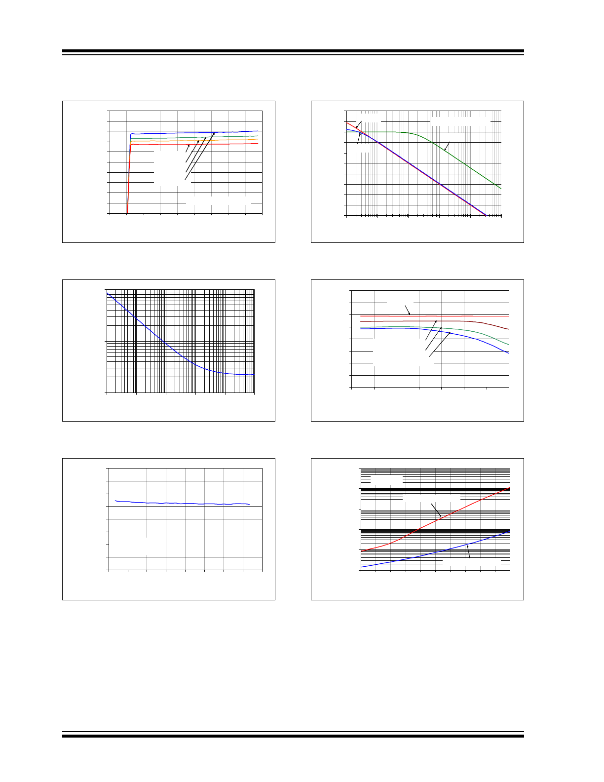
FIGURE 2-7:
Input Offset Voltage vs.
Power Supply Voltage.
FIGURE 2-8:
Input Noise Voltage Density
vs. Frequency.
FIGURE 2-9:
Input Noise Voltage Density
vs. Common Mode Input Voltage.
FIGURE 2-10:
CMRR, PSRR vs.
Frequency.
FIGURE 2-11:
CMRR, PSRR vs. Ambient
Temperature.
FIGURE 2-12:
Input Bias, Offset Currents
vs. Ambient Temperature.
-1000
-800
-600
-400
-200
0
200
400
600
800
1000
0
2
4
6
8
10
12
14
16
18
Power Supply Voltage (V)
In
p
u
t O
ffs
e
t
V
o
lta
g
e
(µ
V
)
T
A
= +125°C
T
A
= +85°C
T
A
= +25°C
T
A
= -40°C
Representative Part
10
100
1,000
1
10
100
1000
10000
100000
Frequency (Hz)
In
p
u
t No
is
e
V
o
lt
ag
e D
en
si
ty
(n
V/
Hz
)
1 10 100 1k 10k 100k
10
15
20
25
30
35
40
45
50
-1
1
3
5
7
9
11
13
15
Common Mode Input Voltage (V)
In
p
u
t
N
o
ise V
o
lt
ag
e D
en
si
ty
(n
V
/
Hz
)
f = 1 kHz
V
DD
= 16V
20
30
40
50
60
70
80
90
100
110
120
10
100
1000
10000
100000 1000000
Frequency (Hz)
C
M
RR,
P
S
R
R
(
d
B)
10 100 1k 10k 100k 1M
CMRR
PSRR+
PSRR-
Representative Part
50
60
70
80
90
100
110
120
130
-50
-25
0
25
50
75
100
125
Ambient Temperature (°C)
CM
RR,
P
S
R
R
(d
B)
PSRR
CMRR @ V
DD
= 15V
@ V
DD
= 5V
@ V
DD
= 3.5V
1
10
100
1000
10000
100000
25
35
45
55
65
75
85
95
10
5
11
5
12
5
Ambient Temperature (°C)
In
p
u
t Bi
as
a
n
d
O
ffs
e
t Cu
rr
en
ts
(A)
Input Bias Current
Input Offset Current
V
DD
= 15V
100n
10n
1n
100p
10p
1p
2010-2011 Microchip Technology Inc.
DS22243D-page 9
MCP6H01/2/4
Note: Unless otherwise indicated, T
A
= +25°C, V
DD
= +3.5V to +16V, V
SS
= GND, V
CM
= V
DD
/2 - 1.4V, V
OUT
V
DD
/2,
V
L
= V
DD
/2, R
L
= 10 k
to V
L
and C
L
= 60 pF.
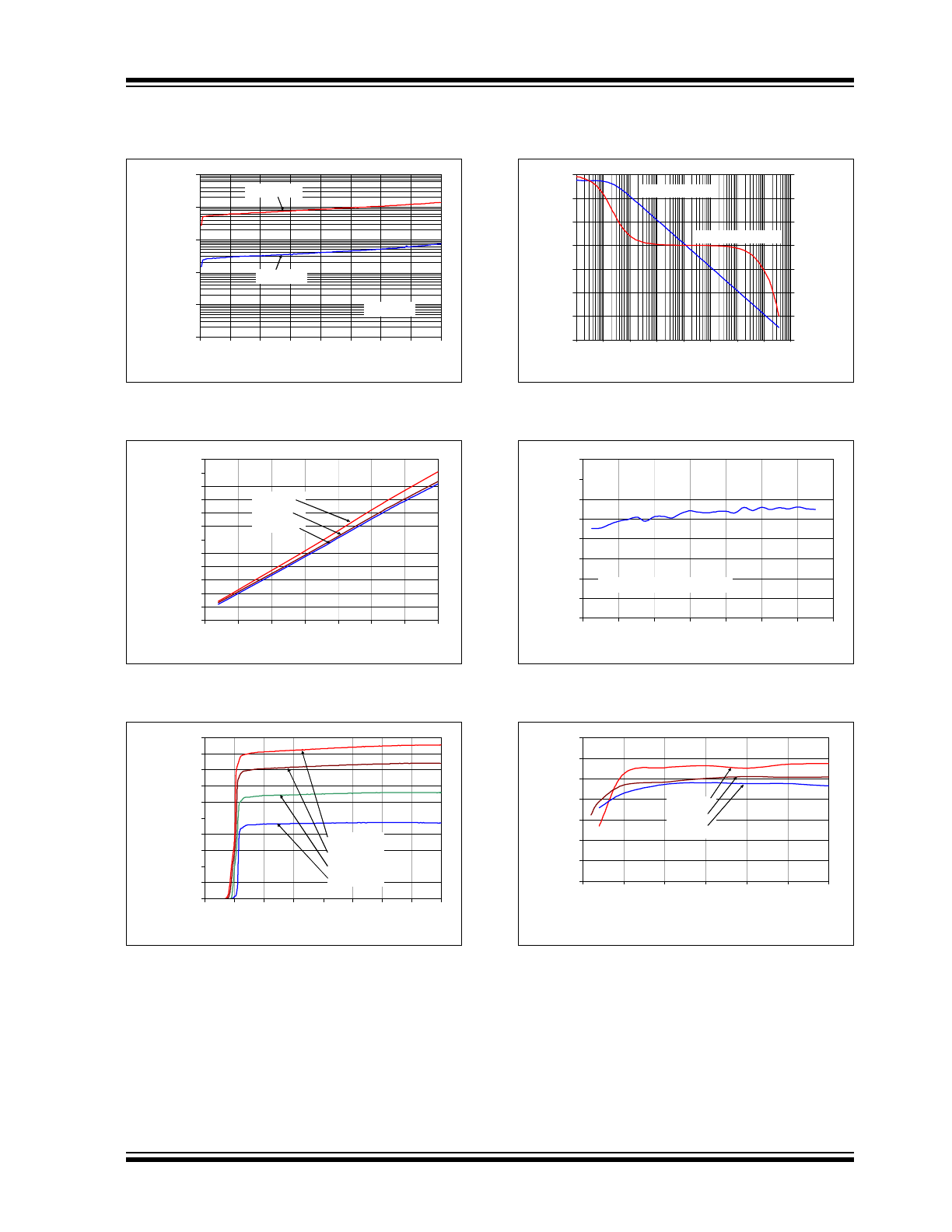
FIGURE 2-13:
Input Bias Current vs.
Common Mode Input Voltage.
FIGURE 2-14:
Quiescent Current vs.
Ambient Temperature.
FIGURE 2-15:
Quiescent Current vs.
Power Supply Voltage.
FIGURE 2-16:
Open-Loop Gain, Phase vs.
Frequency.
FIGURE 2-17:
DC Open-Loop Gain vs.
Power Supply Voltage.
FIGURE 2-18:
DC Open-Loop Gain vs.
Output Voltage Headroom.
1
10
100
1000
10000
100000
0
2
4
6
8
10
12
14
16
Common Mode Input Voltage (V)
In
p
u
t Bi
as
Cu
rr
en
t
(A
)
T
A
= +125°C
T
A
= +85°C
V
DD
= 15V
100n
10n
1n
100p
10p
1p
80
90
100
110
120
130
140
150
160
170
180
190
200
-50
-25
0
25
50
75
100
125
Ambient Temperature (°C)
Q
u
ie
scen
t C
u
rr
en
t
(µ
A
/A
m
p
lif
ie
r)
V
DD
= 15V
V
DD
= 5V
V
DD
= 3.5V
0
20
40
60
80
100
120
140
160
180
200
0
2
4
6
8
10
12
14
16
Power Supply Voltage (V)
Q
u
ie
sc
e
n
t C
u
rren
t
(µ
A
/A
m
p
lif
ie
r)
T
A
= +125°C
T
A
= +85°C
T
A
= +25°C
T
A
= -40°C
-20
0
20
40
60
80
100
120
1.0E-01
1.0E+00 1.0E+01 1.0E+02 1.0E+03 1.0E+04 1.0E+05 1.0E+06 1.0E+07
Frequency (Hz)
Op
en
-L
o
o
p G
ai
n
(
d
B
)
-210
-180
-150
-120
-90
-60
-30
0
O
p
en
-L
oo
p
P
h
as
e (°)
Open-Loop Gain
Open-Loop Phase
0.1 1 10 100 1k 10k 100k 1M 10M
80
90
100
110
120
130
140
150
160
3
5
7
9
11
13
15
17
Power Supply Voltage (V)
D
C
-O
p
en Lo
o
p
G
ain
(
d
B
)
V
SS
+ 0.2V < V
OUT
< V
DD
- 0.2V
80
90
100
110
120
130
140
150
0.00
0.05
0.10
0.15
0.20
0.25
0.30
Output Voltage Headroom (V)
V
DD
- V
OH
or V
OL
- V
SS
DC-
O
p
en
L
o
o
p
G
ai
n
(d
B)
V
DD
= 15V
V
DD
= 5V
V
DD
= 3.5V
MCP6H01/2/4
DS22243D-page 10
2010-2011 Microchip Technology Inc.
Note: Unless otherwise indicated, T
A
= +25°C, V
DD
= +3.5V to +16V, V
SS
= GND, V
CM
= V
DD
/2 - 1.4V, V
OUT
V
DD
/2,
V
L
= V
DD
/2, R
L
= 10 k
to V
L
and C
L
= 60 pF.
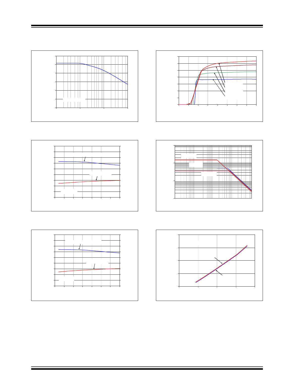
FIGURE 2-19:
Channel-to-Channel
Separation vs. Frequency (MCP6H02 only).
FIGURE 2-20:
Gain Bandwidth Product,
Phase Margin vs. Ambient Temperature.
FIGURE 2-21:
Gain Bandwidth Product,
Phase Margin vs. Ambient Temperature.
FIGURE 2-22:
Output Short Circuit Current
vs. Power Supply Voltage.
FIGURE 2-23:
Output Voltage Swing vs.
Frequency.
FIGURE 2-24:
Output Voltage Headroom
vs. Output Current.
40
60
80
100
120
140
160
100
1000
10000
100000
Frequency (Hz)
Ch
an
n
el
t
o
C
h
an
n
el
Se
p
ar
at
io
n
(
d
B
)
100 1k 10k 100k
Input Referred
0.0
0.2
0.4
0.6
0.8
1.0
1.2
1.4
1.6
1.8
-50
-25
0
25
50
75
100 125
Ambient Temperature (°C)
Ga
in
B
and
w
idt
h
P
rod
u
ct
(M
H
z)
0
20
40
60
80
100
120
140
160
180
P
h
as
e M
argi
n
(°
)
Gain Bandwidth Product
Phase Margin
V
DD
= 3.5V
0.0
0.2
0.4
0.6
0.8
1.0
1.2
1.4
1.6
1.8
-50
-25
0
25
50
75
100 125
Ambient Temperature (°C)
Ga
in
B
and
wi
dt
h
P
rod
u
ct
(M
H
z)
0
20
40
60
80
100
120
140
160
180
Pha
se
M
a
rg
in
(°
)
Gain Bandwidth Product
Phase Margin
V
DD
= 15V
0
10
20
30
40
50
60
70
0
2
4
6
8
10
12
14
16
Power Supply Voltage (V)
Out
p
u
t
S
h
ort
C
ircu
it
C
u
rren
t
(mA
)
T
A
= +125°C
T
A
= +85°C
T
A
= +25°C
T
A
= -40°C
0.1
1
10
100
100
1000
10000
100000
1000000
Frequency (Hz)
O
u
tp
ut
V
o
lt
ag
e S
w
in
g
(
V
P-
P
)
V
DD
= 3.5V
V
DD
= 5V
100 1k 10k 100k 1M
V
DD
= 15V
1
10
100
1000
10000
0.01
0.1
1
10
100
Output Current (mA)
Out
p
u
t V
o
lt
ag
e H
ead
ro
o
m
(
m
V
)
V
DD
- V
OH
V
OL
- V
SS
V
DD
= 15V