
2010-2011 Microchip Technology Inc.
DS22269B-page 1
MCP65R41/6
Features:
• Factory Set Reference Voltage
- Available Voltage: 1.21V and 2.4V
- Tolerance: ±1% (typical)
• Low Quiescent Current: 2.5 µA (typical)
• Propagation Delay: 4 µs with 100 mV Overdrive
• Input Offset Voltage: ±3mV (typical)
• Rail-to-Rail Input: V
SS
- 0.3V to V
DD
+ 0.3V
• Output Options:
- MCP65R41
Push-Pull
- MCP65R46
Open-Drain
• Wide Supply Voltage Range: 1.8V to 5.5V
• Packages: SOT23-6
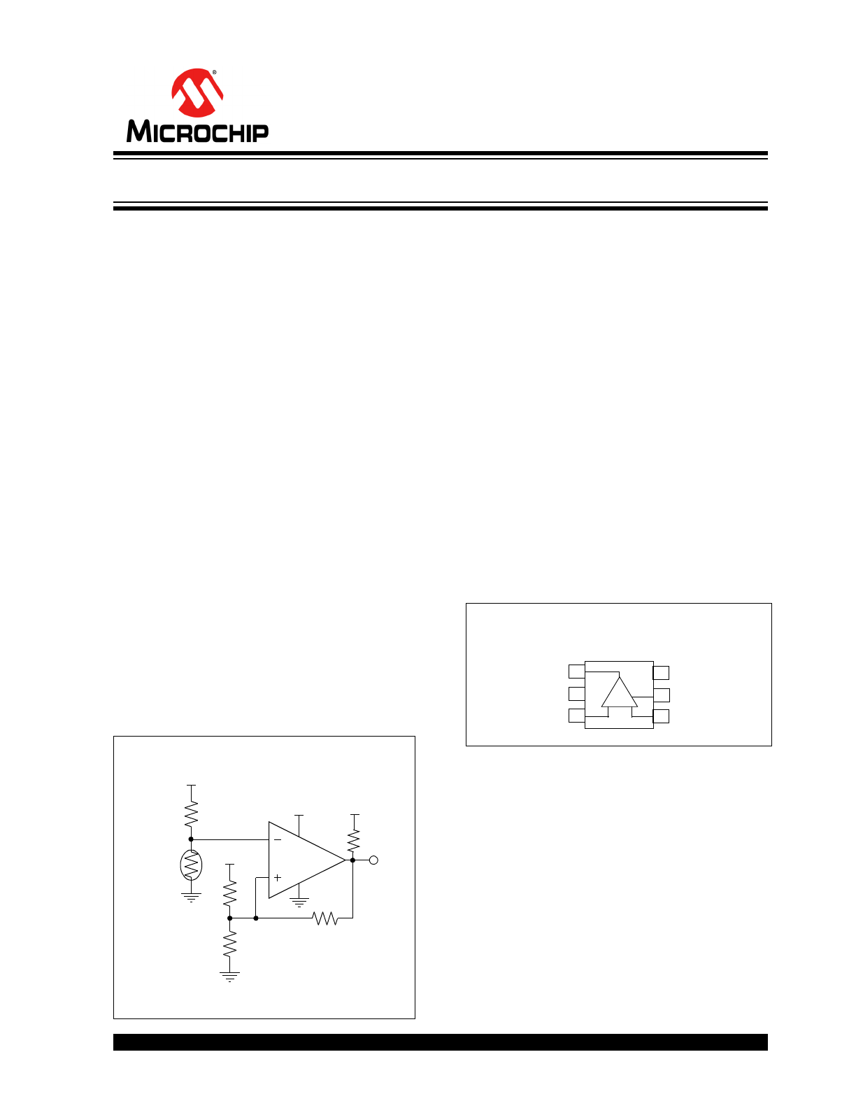
Typical Applications:
• Laptop Computers
• Mobile Phones
• Hand-held Metering Systems
• Hand-held Electronics
• RC Timers
• Alarm and Monitoring Circuits
• Window Comparators
Design Aids:
• Microchip Advanced Part Selector (MAPS)
• Analog Demonstration and Evaluation Boards
Typical Application
Description:
The Microchip Technology Inc. MCP65R41/6 family of
push-pull and open-drain output comparators are
offered with integrated reference voltages of 1.21V and
2.4V. This family provides ±1% (typical) tolerance while
consuming 2.5 µA (typical) current. These comparators
operate with a single-supply voltage as low as 1.8V to
5.5V, which makes them ideal for low cost and/or
battery powered applications.
These comparators are optimized for low-power,
single-supply applications with greater than rail-to-rail
input operation. The output limits supply current surges
and dynamic power consumption while switching. The
internal input hysteresis eliminates output switching
due to internal noise voltage, reducing current draw.
The MCP65R41 output interfaces to CMOS/TTL logic.
The open-drain output device MCP65R46 can be used
as a level-shifter from 1.6V to 10V using a pull-up
resistor. It can also be used as a wired-OR logic.
This family of devices is available in the 6-lead SOT-23
package.
Package Types
V
OUT
V
DD
R
2
R
F
R
3
V
REF
V
PU
R
PU
*
* Pull-up resistor required for the MCP65R46 only.
R
4
Thermistor
V
REF
Over-Temperature Alert
6
4
SOT23-6
MCP65R41/6
1
2
3
-
+
5
OUT
V
SS
+IN
V
DD
V
REF
-IN
3 µA Comparator with Integrated Reference Voltage

MCP65R41/6
DS22269B-page 2
2010-2011 Microchip Technology Inc.
NOTES:
2010-2011 Microchip Technology Inc.
DS22269B-page 3
MCP65R41/6
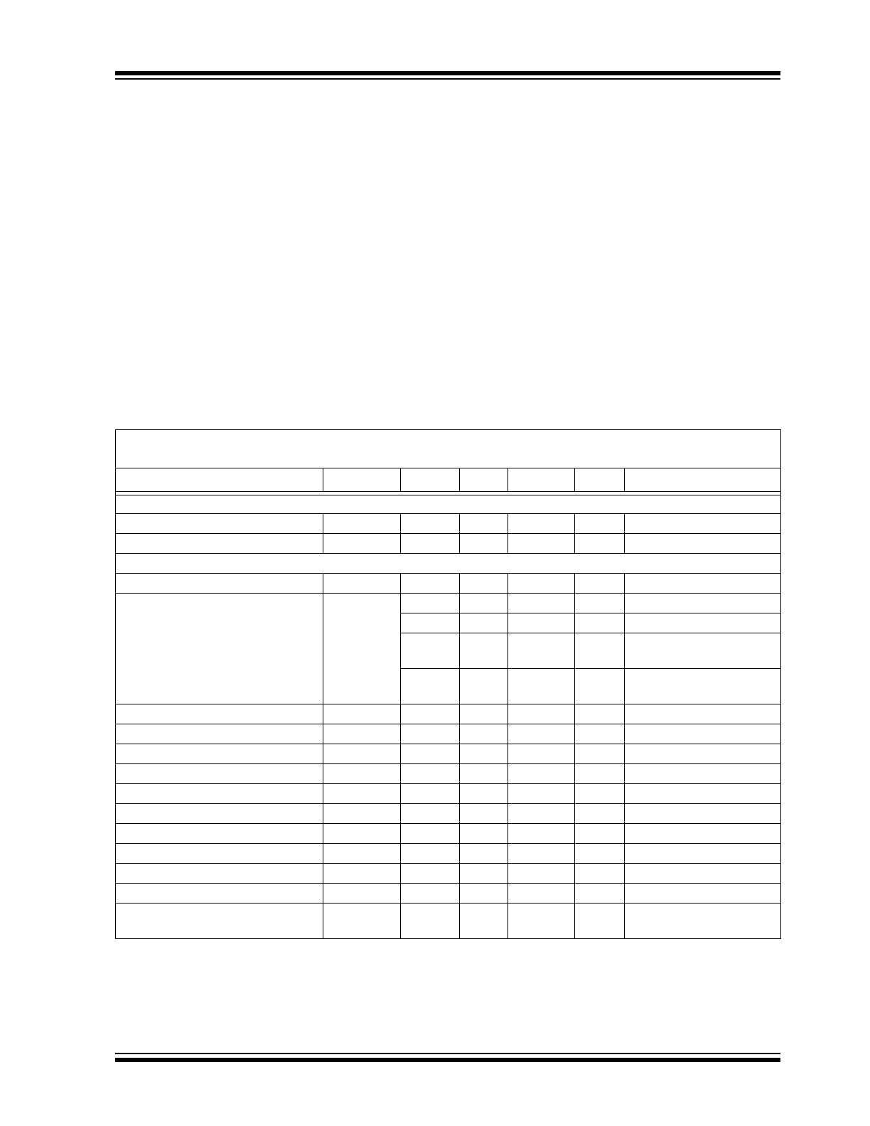
1.0
ELECTRICAL
CHARACTERISTICS
1.1
Absolute Maximum Ratings†
V
DD
- V
SS
....................................................................... 7.0V
All other inputs and outputs...........V
SS
– 0.3V to V
DD
+ 0.3V
Difference Input voltage ......................................|V
DD
- V
SS
|
Output Short Circuit Current .................................... ±25 mA
Current at Input Pins .................................................. ±2 mA
Current at Output and Supply Pins .......................... ±50 mA
Storage temperature ................................... -65°C to +150°C
Ambient temperature with power applied.... -40°C to +125°C
Junction temperature ................................................ +150°C
ESD protection on all pins (HBM/MM)
4 kV/200V
ESD protection on MCP65R46 OUT pin (HBM/MM).............
4 kV/175V
†Notice: Stresses above those listed under “Maximum
Ratings” may cause permanent damage to the device.
This is a stress rating only and functional operation of
the device at those or any other conditions above those
indicated in the operational listings of this specification
is not implied. Exposure to maximum rating conditions
for extended periods may affect device reliability.
DC CHARACTERISTICS
Unless otherwise indicated, all limits are specified for: V
DD
= +1.8V to +5.5V, V
SS
= GND, T
A
= +25°C, V
IN+
=
V
DD
/2, V
IN-
= V
SS
, R
L
= 100 k
to V
DD
/2 (MCP65R41 only), and R
Pull-Up
= 2.74 k
to V
DD
(MCP65R46 only).
Parameters
Sym
Min
Typ
Max
Units
Conditions
Power Supply
Supply Voltage
V
DD
1.8
—
5.5
V
Quiescent Current per Comparator
I
Q
—
2.5
4
µA
I
OUT
= 0
Input
Input Voltage Range
V
CMR
V
SS
0.3
—
V
DD
+0.3
V
Common-Mode Rejection Ratio
V
DD
= 5V
CMRR
55
70
—
dB
V
CM
= -0.3V to 5.3V
50
65
—
dB
V
CM
= 2.5V to 5.3V
55
70
—
dB
MCP65R41,
V
CM
= -0.3V to 2.5V
50
70
—
dB
MCP65R46,
V
CM
= -0.3V to 2.5V
Power Supply Rejection Ratio
PSRR
63
80
—
dB
V
CM
= V
SS
Input Offset Voltage
V
OS
-10
±3
+10
mV
V
CM
= V
SS
(
Note 1
)
Drift with Temperature
V
OS
/
T
—
±10
—
µV/°C V
CM
= V
SS
Input Hysteresis Voltage
V
HYST
1
3.3
5
mV
V
CM
= V
SS
(
Note 1
)
Drift with Temperature
V
HYST
/
T
—
6
—
µV/°C V
CM
= V
SS
Drift with Temperature
V
HYST
/
T
2
—
5
—
µV/°C
2
V
CM
= V
SS
Input Bias Current
I
B
—
1
—
pA
V
CM
=
V
SS
T
A
= +85°C
I
B
—
50
—
pA
V
CM
= V
SS
T
A
= +125°C
I
B
—
—
5000
pA
V
CM
= V
SS
Input Offset Current
I
OS
—
±1
—
pA
V
CM
=
V
SS
Common Mode/
Differential Input Impedance
Z
CM
/Z
DIFF
—
10
13
||4
—
||pF
Note 1:
The input offset voltage is the center (average) of the input-referred trip points. The input hysteresis is the
difference between the input-referred trip points.
2:
Limit the output current to Absolute Maximum Rating of 30 mA.
3:
Do not short the output of the MCP65R46 comparators above V
SS
+ 10V.
4:
The low-power reference voltage pin is designed to drive small capacitive loads. See
Section 4.5.2
.
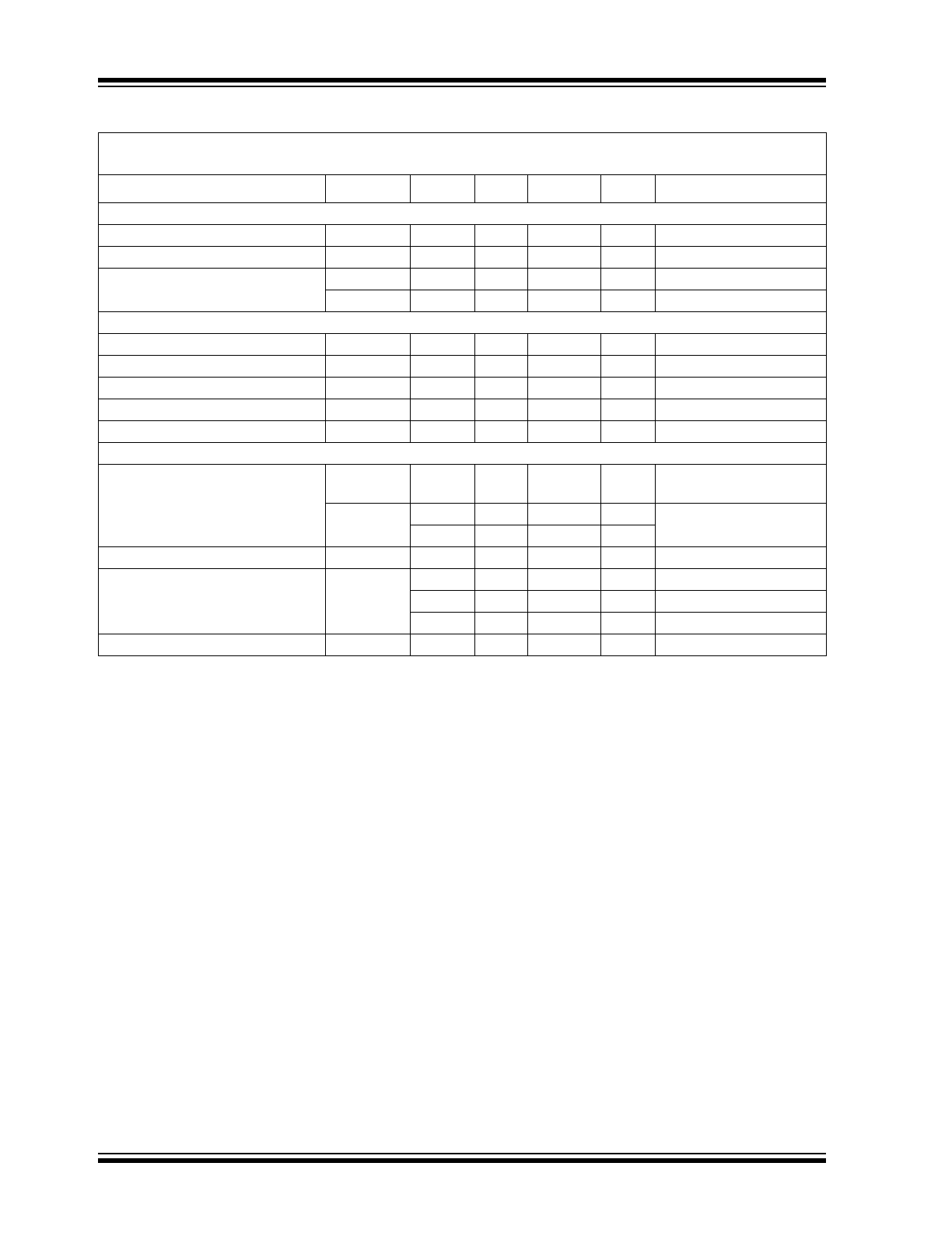
MCP65R41/6
DS22269B-page 4
2010-2011 Microchip Technology Inc.
Push Pull Output
High Level Output Voltage
V
OH
V
DD
0.2
—
—
V
I
OUT
= -2 mA, V
DD
= 5V
Low Level Output Voltage
V
OL
—
—
V
SS
+0.2
V
I
OUT
= 2 mA, V
DD
= 5V
Short Circuit Current
I
SC
—
±50
—
mA
(
Note 2
) MCP65R41
I
SC
—
±1.5
—
mA
(
Note 2
) MCP65R46
Open Drain Output (MCP65R46)
Low Level Output Voltage
V
OL
—
—
V
SS
+0.2
V
I
OUT
= 2 mA
Short Circuit Current
I
SC
—
±50
—
mA
High-Level Output Current
I
OH
-100
—
—
nA
V
PU
= 10V
Pull-up Voltage
V
PU
1.6
—
10
V
Note 3
Output Pin Capacitance
C
OUT
—
8
—
pF
Reference Voltage Output
Initial Reference Tolerance
V
TOL
-2
±1
+2
%
I
REF
= 0A,
V
REF
= 1.21V and 2.4V
V
REF
1.185
1.21
1.234
V
I
REF
= 0A
2.352
2.4
2.448
V
Reference Output Current
I
REF
—
±500
—
µA
V
TOL
= ±2% (maximum)
Drift with Temperature (character-
ized but not production tested)
V
REF
/
T
—
27
100
ppm
V
REF
= 1.21V, V
DD
= 1.8V
—
22
100
ppm
V
REF
= 1.21V, V
DD
= 5.5V
—
23
100
ppm
V
REF
= 2.4V, V
DD
= 5.5V
Capacitive Load
C
L
—
200
—
pF
Note 4
DC CHARACTERISTICS (CONTINUED)
Unless otherwise indicated, all limits are specified for: V
DD
= +1.8V to +5.5V, V
SS
= GND, T
A
= +25°C, V
IN+
=
V
DD
/2, V
IN-
= V
SS
, R
L
= 100 k
to V
DD
/2 (MCP65R41 only), and R
Pull-Up
= 2.74 k
to V
DD
(MCP65R46 only).
Parameters
Sym
Min
Typ
Max
Units
Conditions
Note 1:
The input offset voltage is the center (average) of the input-referred trip points. The input hysteresis is the
difference between the input-referred trip points.
2:
Limit the output current to Absolute Maximum Rating of 30 mA.
3:
Do not short the output of the MCP65R46 comparators above V
SS
+ 10V.
4:
The low-power reference voltage pin is designed to drive small capacitive loads. See
Section 4.5.2
.
2010-2011 Microchip Technology Inc.
DS22269B-page 5
MCP65R41/6
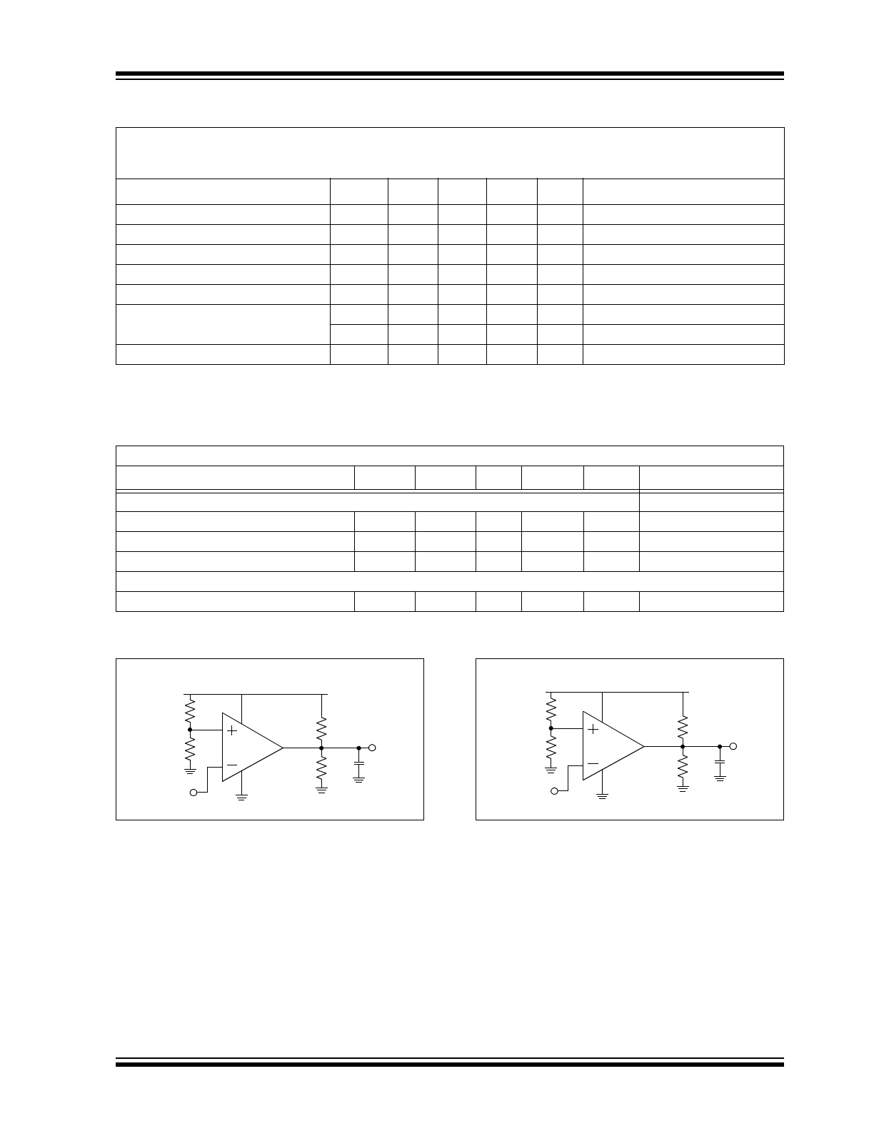
1.2
Test Circuit Configuration
FIGURE 1-1:
Test Circuit for the Push-Pull
Output Comparators.
FIGURE 1-2:
Test Circuit for the Open-
Drain Comparators.
AC CHARACTERISTICS
Unless otherwise indicated, all limits are specified for: V
DD
= +1.8V to +5.5V, V
SS
= GND, T
A
= +25°C,
V
IN+
= V
DD
/2, Step = 200 mV, Overdrive = 100 mV, R
L
= 100 k
to V
DD
/2 (MCP65R41 only),
R
Pull-Up
= 2.74 k
to V
DD
(MCP65R46 only), and C
L
= 50 pF.
Parameters
Sym
Min
Typ
Max
Units
Conditions
Rise Time
t
R
—
0.85
—
µs
Fall Time
t
F
—
0.85
—
µs
Propagation Delay (High-to-Low)
t
PHL
—
4
8.0
µs
Propagation Delay (Low-to-High)
t
PLH
—
4
8.0
µs
Propagation Delay Skew
t
PDS
—
±0.2
—
µs
Note 1
Maximum Toggle Frequency
f
MAX
—
160
—
kHz
V
DD
= 1.8V
f
MAX
—
120
—
kHz
V
DD
= 5.5V
Input Noise Voltage
E
N
—
200
—
µV
P-P
10 Hz to 100 kHz
Note 1:
Propagation Delay Skew is defined as: t
PDS
= t
PLH
- t
PHL
.
TEMPERATURE SPECIFICATIONS
Unless otherwise indicated, all limits are specified for: V
DD
= +1.8V to +5.5V and V
SS
= GND.
Parameters
Symbol
Min
Typ
Max
Units
Conditions
Temperature Ranges
Specified Temperature Range
T
A
-40
—
+125
°C
Operating Temperature Range
T
A
-40
—
+125
°C
Storage Temperature Range
T
A
-65
—
+150
°C
Thermal Package Resistances
Thermal Resistance, SOT23-6
JA
—
190.5
—
°C/W
V
OUT
V
DD
MCP65R41
V
IN
= V
SS
200k
200k
200k
200k
50p
V
SS
= 0V
V
OUT
V
DD
MCP65R46
V
IN
= V
SS
200k
200k
2.74k
100k
50p
V
SS
= 0V

MCP65R41/6
DS22269B-page 6
2010-2011 Microchip Technology Inc.
NOTES:
2010-2011 Microchip Technology Inc.
DS22269B-page 7
MCP65R41/6
2.0
TYPICAL PERFORMANCE CURVES
Note: Unless otherwise indicated, V
DD
= +1.8V to +5.5V, V
SS
= GND, T
A
= +25°C, V
IN
+ = V
DD
/2, V
IN
–
= GND,
R
L
= 100 k
to V
DD
/2 (MCP65R41 only), R
Pull-Up
= 2.74 k
to V
DD
/2 (MCP65R46 only) and C
L
= 50 pF.
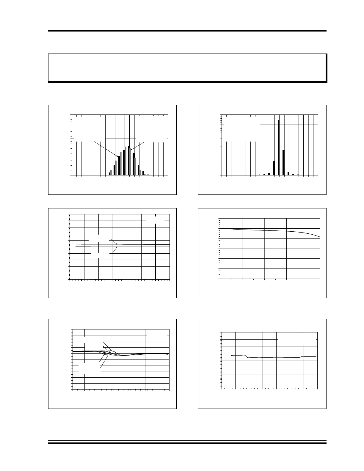
FIGURE 2-1:
Input Offset Voltage.
FIGURE 2-2:
Input Offset Voltage
vs. Temperature.
FIGURE 2-3:
Input Offset Voltage
vs. Common-Mode Input Voltage.
FIGURE 2-4:
Input Offset Voltage Drift.
FIGURE 2-5:
Input Offset Voltage vs.
Supply Voltage vs. Temperature.
FIGURE 2-6:
Input Offset Voltage vs.
Common-Mode Input Voltage.
Note:
The graphs and tables provided following this note are a statistical summary based on a limited number of
samples and are provided for informational purposes only. The performance characteristics listed herein
are not tested or guaranteed. In some graphs or tables, the data presented may be outside the specified
operating range (e.g., outside specified power supply range) and therefore outside the warranted range.
0%
10%
20%
30%
40%
50%
-10 -8
-6
-4
-2
0
2
4
6
8
10
V
OS
(mV)
Oc
cu
rr
en
ce
s (%)
V
DD
= 1.8V
V
CM
= V
SS
Avg. = 1.09 mV
StDev = 1.59 mV
850 units
V
DD
= 5.5V
V
CM
= V
SS
Avg. = 0.61 mV
StDev = 1.48 mV
850 units
-10.0
-8.0
-6.0
-4.0
-2.0
0.0
2.0
4.0
6.0
8.0
10.0
-50
-25
0
25
50
75
100
125
Temperature (°C)
V
DD
= 1.8V
V
DD
= 5.5V
V
CM
= V
SS
V
OS
(mV)
-10.0
-8.0
-6.0
-4.0
-2.0
0.0
2.0
4.0
6.0
8.0
10.0
-0.3
0.0
0.3
0.6
0.9
1.2
1.5
1.8
2.1
V
CM
(V)
V
OS
(m
V
)
V
DD
= 1.8V
T
A
= +25°C
T
A
= +125°C
T
A
= +85°C
T
A
= -40°C
0%
10%
20%
30%
40%
50%
60%
-60 -48 -36 -24 -12
0
12 24 36 48 60
V
OS
Drift (µV/°C)
Oc
cu
rr
en
ce
s (%
)
V
CM
= V
SS
Avg. = 9.86 µV/°C
StDev = 4.97 µV/°C
850 Units
T
A
= -40°C to +125°C
-3.0
-2.0
-1.0
0.0
1.0
2.0
3.0
1.5
2.5
3.5
4.5
5.5
V
DD
(V)
V
OS
(m
V
)
T
A
= -40°C to +125°C
-10.0
-7.5
-5.0
-2.5
0.0
2.5
5.0
7.5
10.0
-1.0
0.0
1.0
2.0
3.0
4.0
5.0
6.0
V
CM
(V)
V
OS
(m
V
)
T
A
= -40°C to +125°C
V
DD
= 5.5V
MCP65R41/6
DS22269B-page 8
2010-2011 Microchip Technology Inc.
Note: Unless otherwise indicated, V
DD
= +1.8V to +5.5V, V
SS
= GND, T
A
= +25°C, V
IN
+ = V
DD
/2, V
IN
–
= GND,
R
L
= 100 k
to V
DD
/2 (MCP65R41 only), R
Pull-Up
= 2.74 k
to V
DD
/2 (MCP65R46 only) and C
L
= 50 pF.
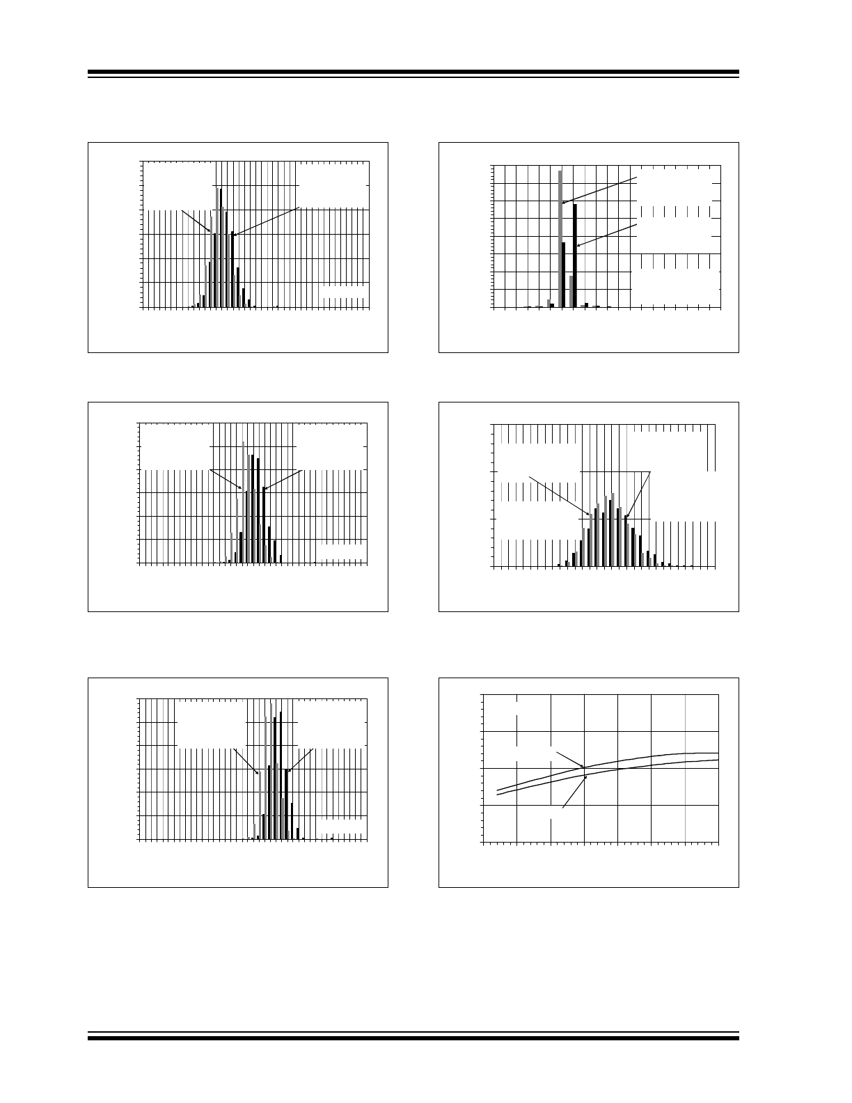
FIGURE 2-7:
Input Hysteresis Voltage
at -40°C.
FIGURE 2-8:
Input Hysteresis Voltage
at +25°C.
FIGURE 2-9:
Input Hysteresis Voltage
at +125°C.
FIGURE 2-10:
Input Hysteresis Voltage
Drift – Linear Temperature Compensation (TC1).
FIGURE 2-11:
Input Hysteresis Voltage
Drift – Quadratic Temperature Compensation
(TC2).
FIGURE 2-12:
Input Hysteresis Voltage
vs. Temperature.
0%
5%
10%
15%
20%
25%
30%
1.0
1.5
2.0
2.5
3.0
3.5
4.0
4.5
5.0
V
HYST
(mV)
Oc
c
u
rr
en
ce
s (
%
)
V
DD
= 1.8V
Avg. = 2.4 mV
StDev = 0.17 mV
850 units
V
DD
= 5.5V
Avg. = 2.3 mV
StDev = 0.17 mV
850 units
T
A
= -40°C
0%
5%
10%
15%
20%
25%
30%
1.0
1.5
2.0
2.5
3.0
3.5
4.0
4.5
5.0
V
HYST
(mV)
O
ccu
rr
en
ces
(
%
)
V
DD
= 1.8V
Avg. = 3.0 mV
StDev = 0.17 mV
850 units
V
DD
= 5.5V
Avg. = 2.8 mV
StDev = 0.17 mV
850 units
T
A
= +25°C
0%
5%
10%
15%
20%
25%
30%
1.0
1.5
2.0
2.5
3.0
3.5
4.0
4.5
5.0
V
HYST
(mV)
O
ccu
rr
en
ces
(
%
)
V
DD
= 1.8V
Avg. = 3.4 mV
StDev = 0.14 mV
850 units
V
DD
= 5.5V
Avg. = 3.2 mV
StDev = 0.13 mV
850 units
T
A
= +125°C
0%
10%
20%
30%
40%
50%
60%
70%
80%
0
2
4
6
8
10 12 14 16 18 20
V
HYST
Drift, TC1 (µV/°C)
O
ccu
rr
en
ce
s (
%
)
850 Units
T
A
= -40°C to +125°C
V
CM
= V
SS
V
DD
= 5.5V
Avg. = 5.7 µV/°C
StDev = 0.50 µV/°C
V
DD
= 1.8V
Avg. = 6.1 µV/°C
StDev = 0.55 µV/°C
0%
10%
20%
30%
-0.50
-0.25
0.00
0.25
0.50
0.75
1.00
V
HYST
Drift, TC2 (µV/°C
2
)
Oc
cu
rr
en
ce
s (%
)
V
DD
= 5.5V
V
CM
= V
SS
Avg. = 10.4 µV/°C
StDev = 0.6 µV/°C
V
DD
= 5.5V
Avg. = 0.25 µV/°C
2
StDev = 0.1 µV/°C
2
V
DD
= 1.8V
Avg. = 0.3 µV/°C
2
StDev = 0.2 µV/°C
2
1380 Units
T
A
= -40°C to +125°C
V
CM
= V
SS
1.0
2.0
3.0
4.0
5.0
-50
-25
0
25
50
75
100
125
Temperature
(°C)
V
HY
S
T
(m
V
)
V
DD
= 5.5V
V
DD
= 1.8V
V
CM
= V
SS
2010-2011 Microchip Technology Inc.
DS22269B-page 9
MCP65R41/6
Note: Unless otherwise indicated, V
DD
= +1.8V to +5.5V, V
SS
= GND, T
A
= +25°C, V
IN
+ = V
DD
/2, V
IN
–
= GND,
R
L
= 100 k
to V
DD
/2 (MCP65R41 only), R
Pull-Up
= 2.74 k
to V
DD
/2 (MCP65R46 only) and C
L
= 50 pF.
FIGURE 2-13:
Input Hysteresis Voltage vs.
Common-Mode Input Voltage.
FIGURE 2-14:
Input Hysteresis Voltage vs.
Common-Mode Input Voltage.
FIGURE 2-15:
Input Hysteresis Voltage vs.
Supply Voltage vs. Temperature.
FIGURE 2-16:
Quiescent Current.
FIGURE 2-17:
Quiescent Current vs.
Common-Mode Input Voltage.
FIGURE 2-18:
Quiescent Current vs.
Common-Mode Input Voltage.
1.0
2.0
3.0
4.0
5.0
-0.3
0.0
0.3
0.6
0.9
1.2
1.5
1.8
2.1
V
CM
(V)
V
HY
S
T
(m
V)
V
DD
= 1.8V
T
A
= +125°C
T
A
= +85°C
T
A
= +25°C
T
A
= -40°C
1.0
2.0
3.0
4.0
5.0
-0.5
0.5
1.5
2.5
3.5
4.5
5.5
V
CM
(V)
V
HY
S
T
(m
V
)
V
DD
= 5.5V
T
A
= -40°C
T
A
= +25°C
T
A
= +85°C
T
A
= +125°C
1.0
2.0
3.0
4.0
5.0
1.5
2.5
3.5
4.5
5.5
V
DD
(V)
V
H
YST
(m
V
)
T
A
= -40°C
T
A
= +25°C
T
A
= +85°C
T
A
= +125°C
0%
10%
20%
30%
40%
50%
60%
70%
80%
90%
100%
0.0
1.0
2.0
3.0
4.0
5.0
I
Q
(µV/V)
Oc
c
u
rr
en
ce
s (
%
)
V
DD
= 1.8V
850 units
Temp +125°C
Avg. = 3.51 µA
StDev= 0.07 µA
Temp +85°C
Avg. = 3 µA
StDev= 0.07 µA
Temp +25°C
Avg. = 2.52 µA
StDev= 0.08 µA
Temp -40°C
Avg. = 1.93 µA
StDev= 0.08 µA
2.0
2.1
2.2
2.3
2.4
2.5
2.6
2.7
2.8
2.9
3.0
-0.5
0.0
0.5
1.0
1.5
2.0
2.5
V
CM
(V)
I
Q
(µ
A)
V
DD
= 1.8V
Sweep V
IN
- ,V
IN+
=
Sweep V
IN+
,V
IN
- = V
DD
/2
Sweep V
IN
- ,V
IN+
= V
DD
/2
2.0
2.1
2.2
2.3
2.4
2.5
2.6
2.7
2.8
2.9
3.0
-1.0
0.0
1.0
2.0
3.0
4.0
5.0
6.0
V
CM
(V)
I
Q
(µ
A)
V
DD
= 5.5V
Sweep V
IN
- ,V
IN+
= V
DD
/2
Sweep V
IN+
,V
IN-
= V
DD
/2
MCP65R41/6
DS22269B-page 10
2010-2011 Microchip Technology Inc.
Note: Unless otherwise indicated, V
DD
= +1.8V to +5.5V, V
SS
= GND, T
A
= +25°C, V
IN
+ = V
DD
/2, V
IN
–
= GND,
R
L
= 100 k
to V
DD
/2 (MCP65R41 only), R
Pull-Up
= 2.74 k
to V
DD
/2 (MCP65R46 only) and C
L
= 50 pF.
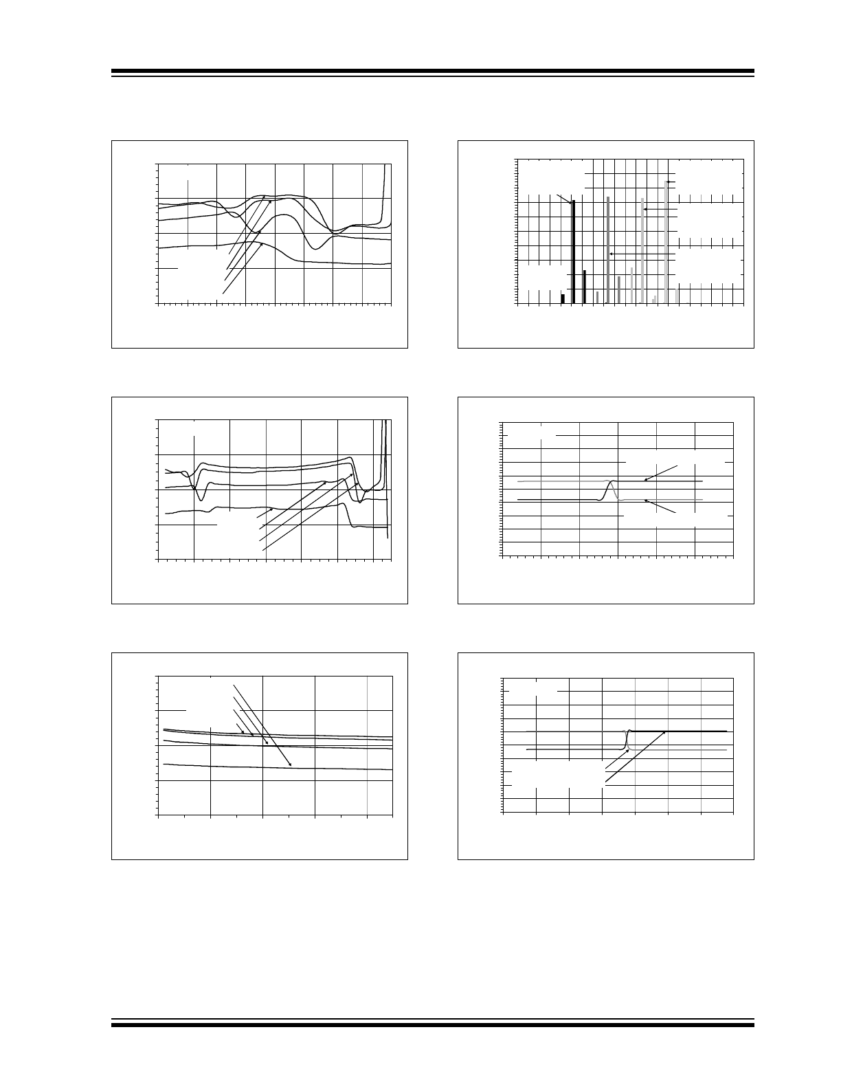
FIGURE 2-19:
Quiescent Current vs.
Supply Voltage vs. Temperature.
FIGURE 2-20:
Quiescent Current vs.
Toggle Frequency.
FIGURE 2-21:
Short Circuit Current vs.
Supply Voltage vs. Temperature.
FIGURE 2-22:
Quiescent Current vs.
Common-Mode Input Voltage.
FIGURE 2-23:
Quiescent Current vs. Pull-
Up Voltage.
FIGURE 2-24:
No Phase Reversal.
0.0
0.5
1.0
1.5
2.0
2.5
3.0
3.5
4.0
4.5
0.0
1.0
2.0
3.0
4.0
5.0
6.0
V
DD
(V)
I
Q
(µ
A)
T
A
= -40°C
T
A
= +25°C
T
A
= +85°C
T
A
= +125°C
0
2
4
6
8
10
12
14
16
18
10
100
1000
10000
100000
Toggle Frequency (Hz)
I
Q
(µ
A)
V
DD
= 5.5V
V
DD
= 1.8V
10
100
1k
10k
100k
100 mV Over-Drive
V
CM
= V
DD
/2
R
L
= Open
0 dB Output Attenuation
-120
-80
-40
0
40
80
120
0.0
1.0
2.0
3.0
4.0
5.0
6.0
V
DD
(V)
I
SC
(m
A
)
T
A
= -40°C
T
A
= +85°C
T
A
= +25°C
T
A
= +125°C
T
A
= -40°C
T
A
= +85°C
T
A
= +25°C
0.0
0.5
1.0
1.5
2.0
2.5
3.0
3.5
4.0
-1.0
0.0
1.0
2.0
3.0
4.0
5.0
6.0
V
CM
(V)
I
Q
(m
A)
V
DD
= 5.5V
Sweep V
IN+
,V
IN
- = V
DD
/2
Sweep V
IN
- ,V
IN+
= V
DD
/2
MCP65R46
1.0
2.0
3.0
4.0
5.0
6.0
7.0
8.0
9.0
10.0
0
1
2
3
4
5
6
7
8
9
10
V
PU
(V)
I
Q
(µA
)
V
DD
= 2.5V
V
DD
= 1.8V
V
DD
= 5.5V
V
DD
= 4.5V
V
DD
= 3.5V
MCP65R46
-1.0
0.0
1.0
2.0
3.0
4.0
5.0
6.0
7.0
Time (3 µs/div)
V
OU
T
(V
)
V
IN
-
V
OUT
V
DD
= 5.5V
V
IN
+ = V
DD
/2