
2009-2013 Microchip Technology Inc.
DS22139C-page 1
MCP6561/1R/1U/2/4
Features
• Propagation Delay at 1.8V
DD
:
- 56 ns (typical) High-to-Low
- 49 ns (typical) Low-to-High
• Low Quiescent Current: 100 µA (typical)
• Input Offset Voltage: ±3 mV (typical)
• Rail-to-Rail Input: V
SS
- 0.3V to V
DD
+ 0.3V
• CMOS/TTL-Compatible Output
• Wide Supply Voltage Range: 1.8V to 5.5V
• Available in Single, Dual, and Quad
• Packages: SC70-5, SOT-23-5, SOIC, MSOP,
TSSOP
Typical Applications
• Laptop Computers
• Mobile Phones
• Hand-held Electronics
• RC Timers
• Alarm and Monitoring Circuits
• Window Comparators
• Multivibrators
Design Aids
• Microchip Advanced Part Selector (MAPS)
• Analog Demonstration and Evaluation Boards
• Application Notes
Related Devices
• Open-Drain Output: MCP6566/6R/6U/7/9
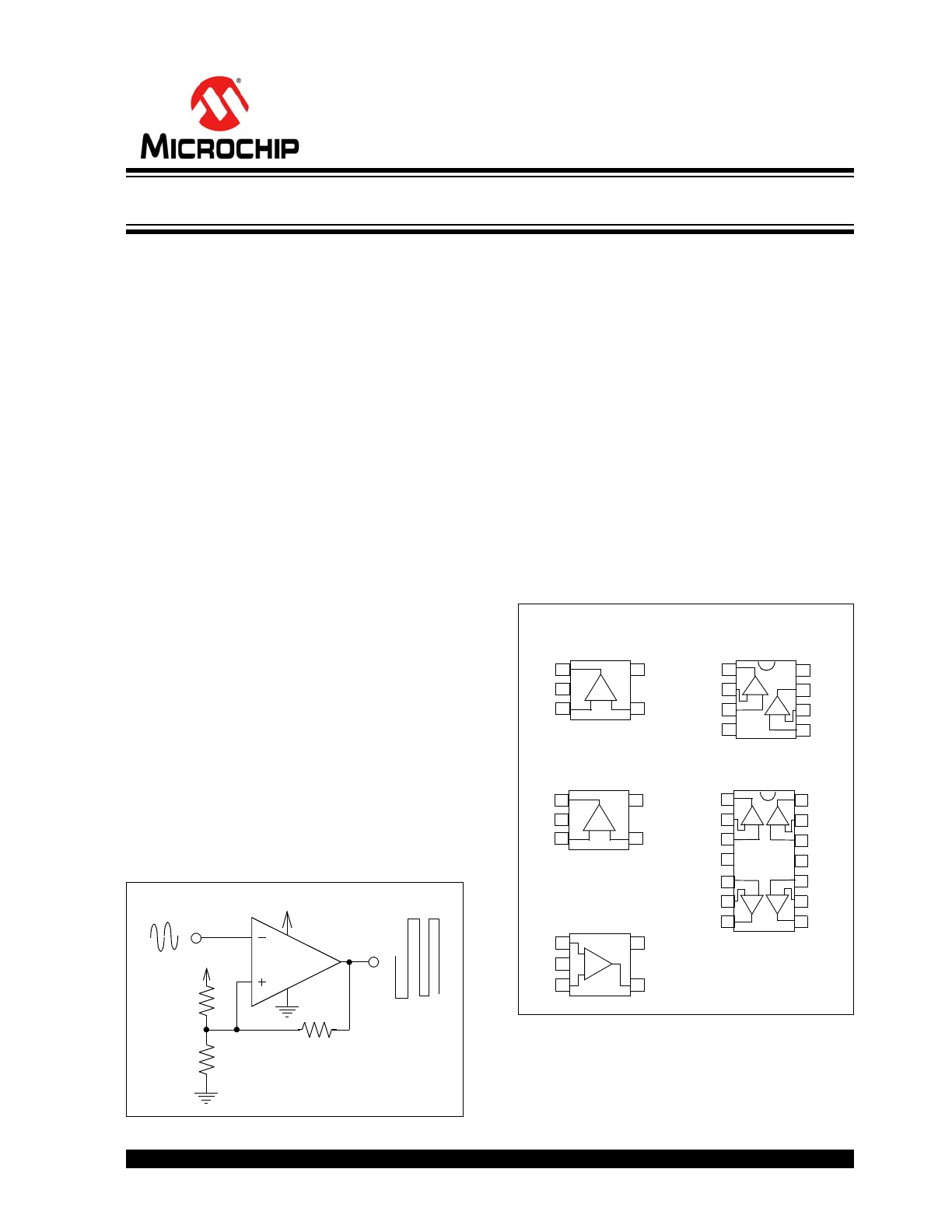
Typical Application
Description
The Microchip Technology, Inc. MCP6561/1R/1U/2/4
families of CMOS/TTL compatible comparators are
offered in single, dual, and quad configurations.
These comparators are optimized for low power 1.8V,
single-supply applications with greater than rail-to-rail
input operation. The internal input hysteresis eliminates
output switching due to internal input noise voltage,
reducing current draw. The push-pull output of the
MCP6561/1R/1U/2/4 family supports rail-to-rail output
swing, and interfaces with CMOS/TTL logic. The output
toggle frequency can reach a typical of 4 MHz (typical)
while limiting supply current surges and dynamic power
consumption during switching.
This family operates with single supply voltage of 1.8V
to 5.5V while drawing less than 100 µA/comparator of
quiescent current (typical).
Package Types
V
IN
V
OUT
V
DD
R
2
R
F
R
3
V
DD
MCP656X
MCP6562
+INA
-INA
V
SS
1
2
3
4
8
7
6
5
-
OUTA
+
-
+
V
DD
OUTB
-INB
+INB
MCP6564
+INA
-INA
V
SS
1
2
3
4
14
13
12
11
-
OUTA
+ -
+
V
DD
OUTD
-IND
+IND
10
9
8
5
6
7
OUTB
-INB
+INB
+INC
-INC
OUTC
+
-
-
+
5
4
MCP6561
1
2
3
-
+
5
4
MCP6561R
1
2
3
-
+
+IN
V
SS
OUT
-IN
V
DD
+IN
V
DD
OUT
-IN
V
SS
SOT-23-5, SC70-5
SOIC, MSOP
SOT-23-5
SOIC, TSSOP
4
1
2
3
5
SOT-23-5
V
SS
V
IN
+
V
IN
–
V
DD
OUT
MCP6561U
-
+
1.8V Low-Power Push-Pull Output Comparator

MCP6561/1R/1U/2/4
DS22139C-page 2
2009-2013 Microchip Technology Inc.
NOTES:
2009-2013 Microchip Technology Inc.
DS22139C-page 3
MCP6561/1R/1U/2/4
1.0
ELECTRICAL
CHARACTERISTICS
1.1
Maximum Ratings †
V
DD
- V
SS
....................................................................... 6.5V
Analog Input (V
IN
) †† .....................V
SS
- 1.0V to V
DD
+ 1.0V
All other inputs and outputs............V
SS
- 0.3V to V
DD
+ 0.3V
Difference Input voltage ......................................|V
DD
- V
SS
|
Output Short Circuit Current .................................... ±25 mA
Current at Input Pins .................................................. ±2 mA
Current at Output and Supply Pins .......................... ±50 mA
Storage temperature ................................... -65°C to +150°C
Ambient temp. with power applied .............. -40°C to +125°C
Junction temp............................................................ +150°C
ESD protection on all pins (HBM/MM)
4 kV/300V
† Notice: Stresses above those listed under “Maximum Rat-
ings” may cause permanent damage to the device. This is a
stress rating only and functional operation of the device at
those or any other conditions above those indicated in the
operational listings of this specification is not implied. Expo-
sure to maximum rating conditions for extended periods may
affect device reliability.
†† See
Section 4.1.2 “Input Voltage and Current Limits”
DC CHARACTERISTICS
Electrical Characteristics: Unless otherwise indicated: V
DD
= +1.8V to +5.5V, V
SS
= GND, T
A
= +25°C, V
IN
+ = V
DD
/2, V
IN
- = V
SS
,
R
L
= 10 k
to V
DD
/2 (see
Figure 1-1
).
Parameters
Symbol
Min
Typ
Max
Units
Conditions
Power Supply
Supply Voltage
V
DD
1.8
—
5.5
V
Quiescent Current per comparator
I
Q
60
100
130
µA
I
OUT
= 0
Power Supply Rejection Ratio
PSRR
63
70
—
dB
V
CM
= V
SS
Input
Input Offset Voltage
V
OS
-10
3
+10
mV
V
CM
= V
SS
(
Note 1
)
Input Offset Drift
V
OS
/
T
—
2
—
µV/°C
V
CM
= V
SS
Input Offset Current
I
OS
—
1
—
pA
V
CM
= V
SS
Input Bias Current
I
B
—
1
—
pA
T
A
= +25°C, V
IN
- = V
DD
/2
—
60
—
pA
T
A
= +85°C, V
IN
- = V
DD
/2
—
1500
5000
pA
T
A
= +125°C, V
IN
- = V
DD
/2
Input Hysteresis Voltage
V
HYST
1.0
—
5.0
mV
V
CM
= V
SS
(
Notes 1
,
2
)
Input Hysteresis Linear Temp. Co.
TC
1
—
10
—
µV/°C
Input Hysteresis Quadratic Temp.
Co.
TC
2
—
0.3
—
µV/°C
2
Common-mode Input Voltage
Range
V
CMR
V
SS
0.2
—
V
DD
+0.2
V
V
DD
= 1.8V
V
SS
0.3
—
V
DD
+0.3
V
V
DD
= 5.5V
Common-mode Rejection Ratio
CMRR
54
66
—
dB
V
CM
= -0.3V to V
DD
+0.3V, V
DD
= 5.5V
50
63
—
dB
V
CM
= V
DD
/2 to V
DD
+0.3V, V
DD
= 5.5V
54
65
—
dB
V
CM
= -0.3V to V
DD
/2, V
DD
= 5.5V
Common-mode Input Impedance
Z
CM
—
10
13
||4
—
||pF
Differential Input Impedance
Z
DIFF
—
10
13
||2
—
||pF
Push-Pull Output
High-Level Output Voltage
V
OH
V
DD
0.7
—
—
V
I
OUT
= -3 mA/-8 mA with V
DD
= 1.8V/5.5V
(
Note 3
)
Low-Level Output Voltage
V
OL
—
—
0.6
V
I
OUT
= 3 mA/8 mA with V
DD
= 1.8V/5.5V
(
Note 3
)
Short Circuit Current
I
SC
—
±30
—
mA
Note 3
Output Pin Capacitance
C
OUT
—
8
—
pF
Note
1:
The input offset voltage is the center of the input-referred trip points. The input hysteresis is the difference between the
input-referred trip points.
2:
V
HYST
at different temperatures is estimated using V
HYST
(T
A
) = V
HYST @ +25°C
+ (T
A
- 25°C) TC
1
+ (T
A
- 25°C)
2
TC
2
.
3:
Limit the output current to Absolute Maximum Rating of 50 mA.
MCP6561/1R/1U/2/4
DS22139C-page 4
2009-2013 Microchip Technology Inc.
AC CHARACTERISTICS
TEMPERATURE SPECIFICATIONS
1.2
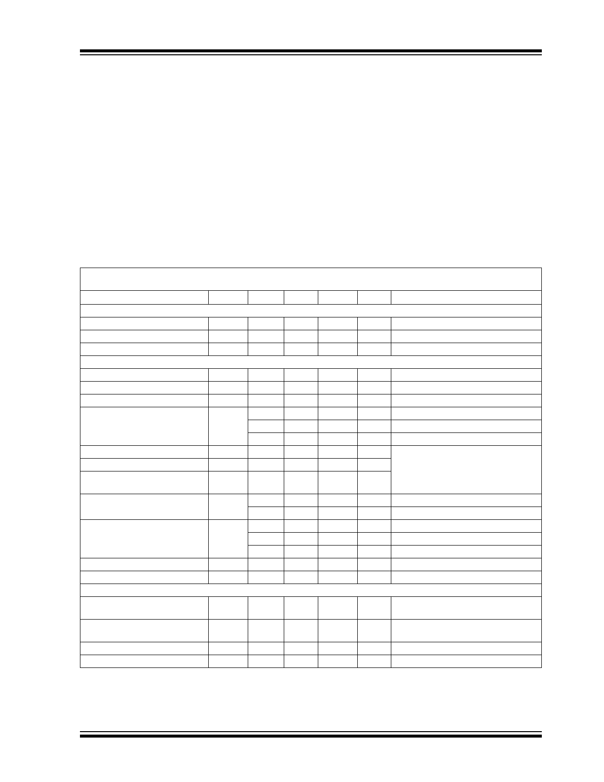
Test Circuit Configuration
This test circuit configuration is used to determine the
AC and DC specifications.
FIGURE 1-1:
AC and DC Test Circuit for
the Push-Pull Output Comparators.
Electrical Characteristics: Unless otherwise indicated: V
DD
= +1.8V to +5.5V, V
SS
= GND, T
A
= +25°C, V
IN
+ = V
DD
/2, V
IN
- = V
SS
,
R
L
= 10 k
to V
DD
/2, and C
L
= 25 pF. (see
Figure 1-1
).
Parameters
Symbol
Min
Typ
Max
Units
Conditions
Propagation Delay
High-to-Low,100 mV Overdrive
t
PHL
—
56
80
ns
V
CM
= V
DD
/2, V
DD
= 1.8V
—
34
80
ns
V
CM
= V
DD
/2, V
DD
= 5.5V
Low-to-High, 100 mV Overdrive
t
PLH
—
49
80
ns
V
CM
= V
DD
/2, V
DD
= 1.8V
—
47
80
ns
V
CM
= V
DD
/2, V
DD
= 5.5V
Skew
1
t
PDS
—
±10
—
ns
Output
Rise Time
t
R
—
20
—
ns
Fall Time
t
F
—
20
—
ns
Maximum Toggle Frequency
f
TG
—
4
—
MHz
V
DD
= 5.5V
—
2
—
MHz
V
DD
= 1.8V
Input Voltage Noise
2
E
NI
—
350
—
µV
P-P
10 Hz to 10 MHz
Note
1:
Propagation Delay Skew is defined as: t
PDS
= t
PLH
- t
PHL
.
2:
ENI is based on SPICE simulation.
Electrical Characteristics: Unless otherwise indicated: V
DD
= +1.8V to +5.5V and V
SS
= GND.
Parameters
Symbol
Min
Typ
Max
Units
Conditions
Temperature Ranges
Specified Temperature Range
T
A
-40
—
+125
°C
Operating Temperature Range
T
A
-40
—
+125
°C
Storage Temperature Range
T
A
-65
—
+150
°C
Thermal Package Resistances
Thermal Resistance, SC70-5
JA
—
331
—
°C/W
Thermal Resistance, SOT-23-5
JA
—
220.7
—
°C/W
Thermal Resistance, 8L-SOIC
JA
—
149.5
—
°C/W
Thermal Resistance, 8L-MSOP
JA
—
211
—
°C/W
Thermal Resistance, 14L-SOIC
JA
—
95.3
—
°C/W
Thermal Resistance, 14L-TSSOP
JA
—
100
—
°C/W
V
DD
V
SS
= 0V
200 k
200 k
200 k
200 k
V
OUT
V
IN
= V
SS
25 pF
I
OUT
MCP656X
2009-2013 Microchip Technology Inc.
DS22139C-page 5
MCP6561/1R/1U/2/4
2.0
TYPICAL PERFORMANCE CURVES
Note: Unless otherwise indicated, V
DD
= +1.8V to +5.5V, V
SS
= GND, T
A
= +25°C, V
IN
+ = V
DD
/2, V
IN
–
= GND,
R
L
= 10 k
to V
DD
/2, and C
L
= 25 pF.
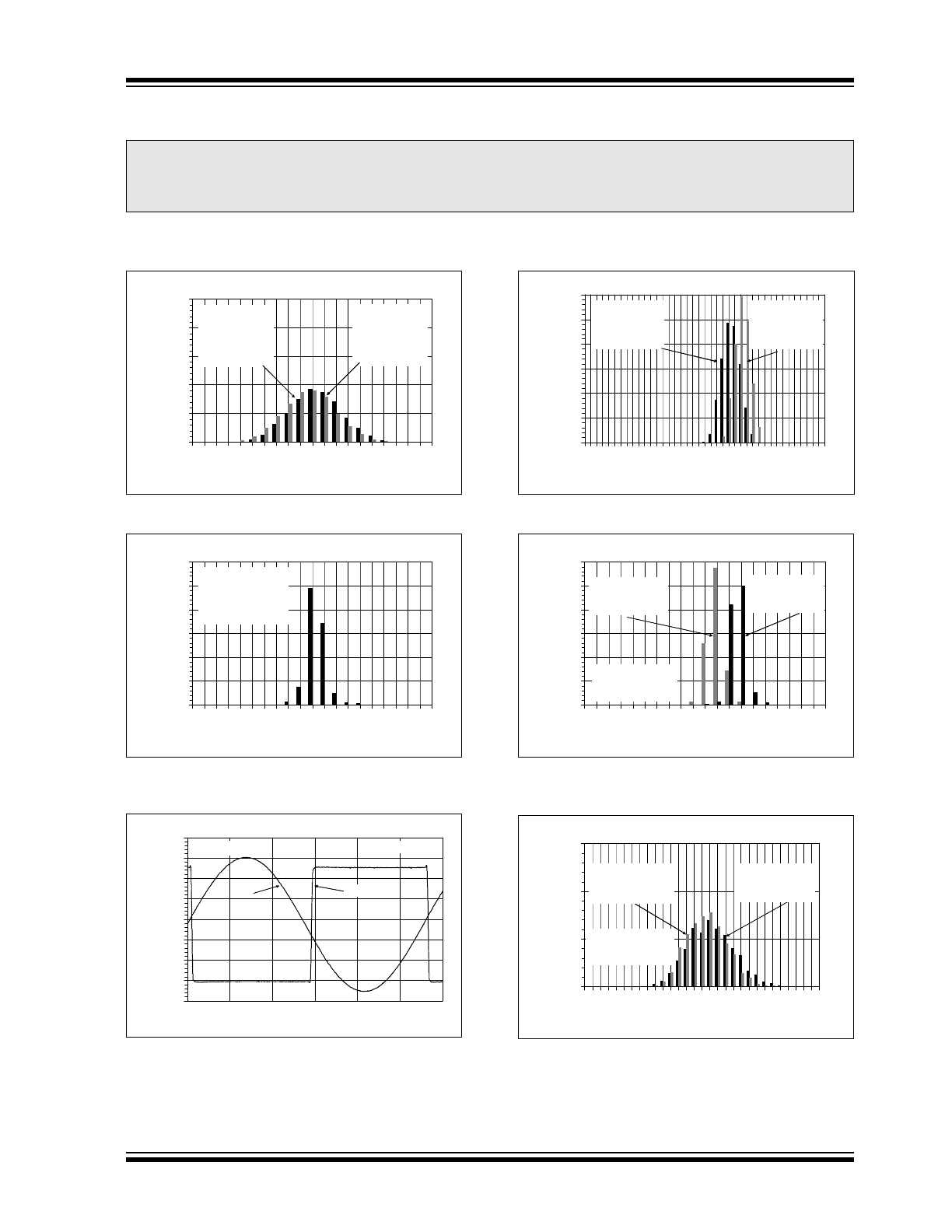
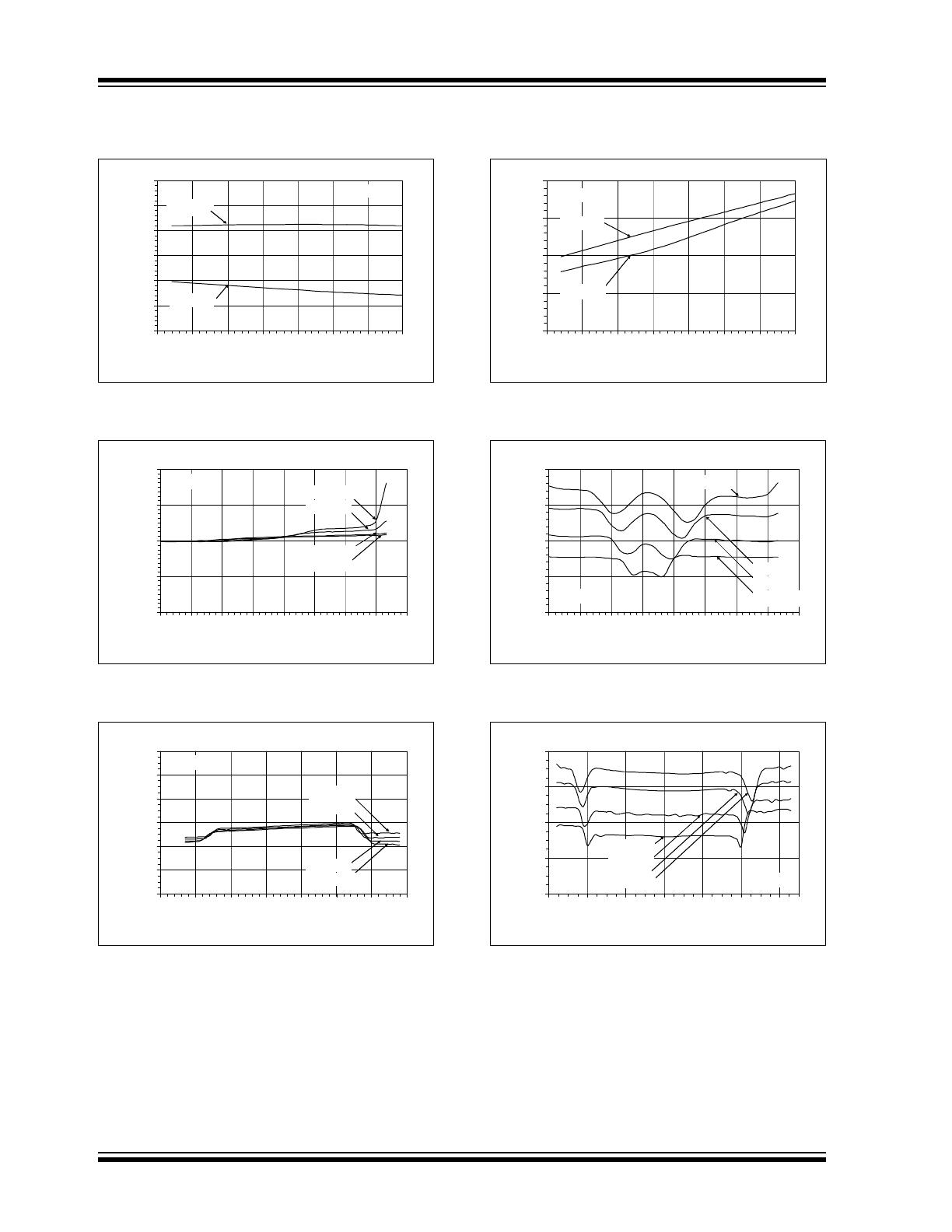
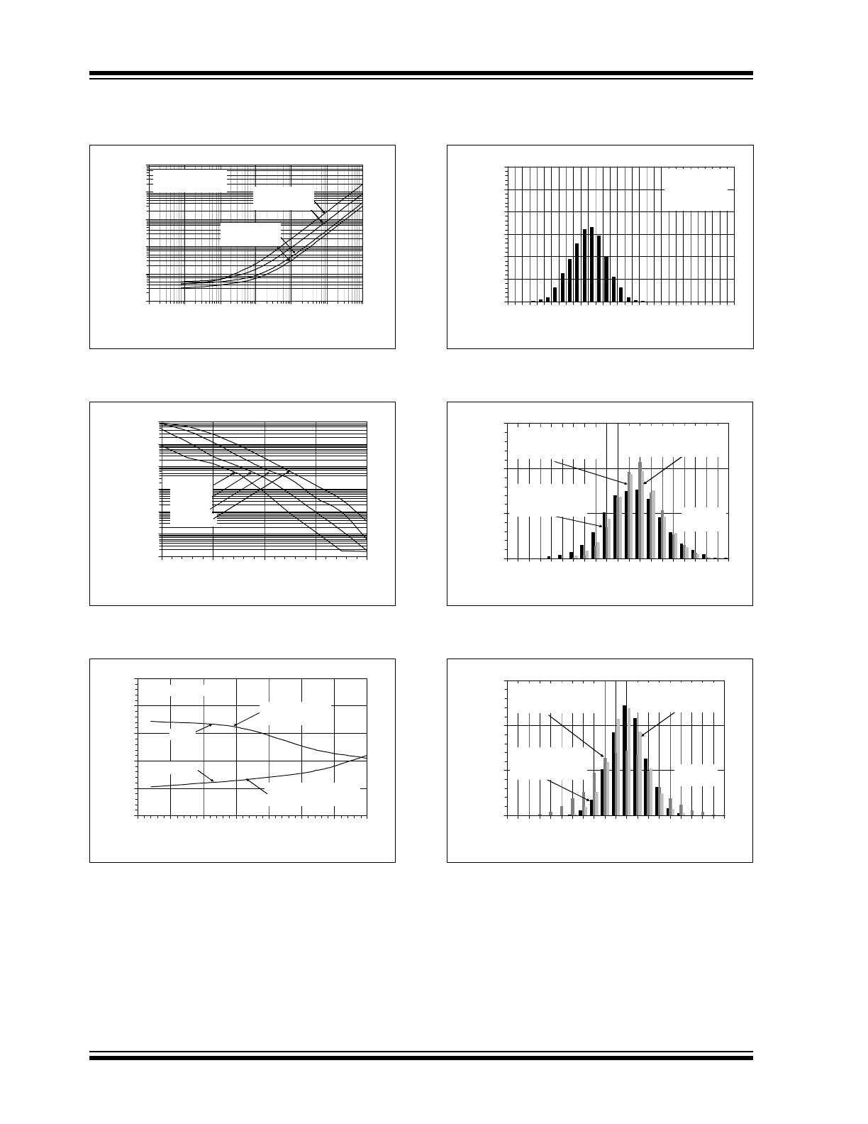
FIGURE 2-1:
Input Offset Voltage.
FIGURE 2-2:
Input Offset Voltage Drift.
FIGURE 2-3:
Input vs. Output Signal, No
Phase Reversal.
FIGURE 2-4:
Input Hysteresis Voltage.
FIGURE 2-5:
Input Hysteresis Voltage
Drift - Linear Temp. Co. (TC1).
FIGURE 2-6:
Input Hysteresis Voltage
Drift - Quadratic Temp. Co. (TC2).
Note:
The graphs and tables provided following this note are a statistical summary based on a limited number of
samples and are provided for informational purposes only. The performance characteristics listed herein
are not tested or guaranteed. In some graphs or tables, the data presented may be outside the specified
operating range (e.g., outside specified power supply range) and therefore outside the warranted range.
0%
10%
20%
30%
40%
50%
-10
-8
-6
-4
-2
0
2
4
6
8
10
V
OS
(mV)
O
c
cu
rr
en
c
e
s
(
%
)
V
DD
= 1.8V
V
CM
= V
SS
Avg. = -0.1 mV
StDev = 2.1 mV
3588 units
V
DD
= 5.5V
V
CM
= V
SS
Avg. = -0.9 mV
StDev = 2.1 mV
3588 units
0%
10%
20%
30%
40%
50%
60%
-60 -48 -36 -24 -12
0
12
24
36
48
60
V
OS
Drift (µV/°C)
O
c
cu
rr
en
c
e
s
(
%
)
V
CM
= V
SS
Avg. = 0.9 µV/°C
StDev = 6.6 µV/°C
1380 Units
T
A
= -40°C to +125°C
-1.0
0.0
1.0
2.0
3.0
4.0
5.0
6.0
7.0
Time (3 µs/div)
V
OU
T
(V)
V
IN
-
V
OUT
V
DD
= 5.5V
V
IN
+ = V
DD
/2
0%
5%
10%
15%
20%
25%
30%
1.0
1.5
2.0
2.5
3.0
3.5
4.0
4.5
5.0
V
HYST
(mV)
O
ccu
rr
e
n
ces (
%
)
V
DD
= 1.8V
Avg. = 3.4 mV
StDev = 0.2 mV
3588 units
V
DD
= 5.5V
Avg. = 3.6 mV
StDev = 0.1 mV
3588 units
0%
10%
20%
30%
40%
50%
60%
0
2
4
6
8
10
12
14
16
18
20
V
HYST
Drift, TC1 (µV/°C)
O
c
cu
rr
en
c
e
s
(
%
)
1380 Units
T
A
= -40°C to 125°C
V
CM
= V
SS
V
DD
= 5.5V
Avg. = 10.4 µV/°C
StDev = 0.6 µV/°C
V
DD
= 1.8V
Avg. = 12 µV/°C
StDev = 0.6 µV/°C
0%
10%
20%
30%
-0.50
-0.25
0.00
0.25
0.50
0.75
1.00
V
HYST
Drift, TC2 (µV/°C
2
)
O
c
cu
rr
en
c
e
s
(
%
)
V
DD
= 5.5V
Avg. = 0.25 µV/°C
2
StDev = 0.1 µV/°C
2
V
DD
= 1.8V
Avg. = 0.3 µV/°C
2
StDev = 0.2 µV/°C
2
1380 Units
T
A
= -40°C to +125°C
V
CM
= V
SS
MCP6561/1R/1U/2/4
DS22139C-page 6
2009-2013 Microchip Technology Inc.
Note: Unless otherwise indicated, V
DD
= +1.8V to +5.5V, V
SS
= GND, T
A
= +25°C, V
IN
+ = V
DD
/2, V
IN
–
= GND,
R
L
= 10 k
to V
DD
/2, and C
L
= 25 pF.
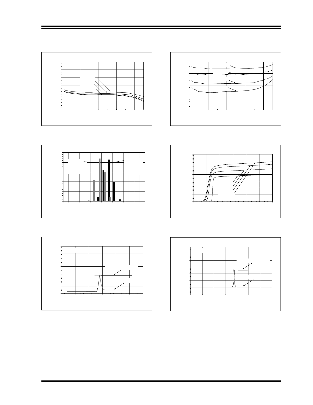
FIGURE 2-7:
Input Offset Voltage vs.
Temperature.
FIGURE 2-8:
Input Offset Voltage vs.
Common-mode Input Voltage.
FIGURE 2-9:
Input Offset Voltage vs.
Common-mode Input Voltage.
FIGURE 2-10:
Input Hysteresis Voltage vs.
Temperature.
FIGURE 2-11:
Input Hysteresis Voltage vs.
Common-mode Input Voltage.
FIGURE 2-12:
Input Hysteresis Voltage vs.
Common-mode Input Voltage.
-3.0
-2.0
-1.0
0.0
1.0
2.0
3.0
-50
-25
0
25
50
75
100
125
Temperature
(°C)
V
OS
(m
V)
V
DD
= 1.8V
V
DD
= 5.5V
V
CM
= V
SS
-4.0
-2.0
0.0
2.0
4.0
-0.3
0.0
0.3
0.6
0.9
1.2
1.5
1.8
2.1
V
CM
(V)
V
OS
(m
V
)
V
DD
= 1.8V
T
A
= +25°C
T
A
= +125°C
T
A
= +85°C
T
A
= -40°C
-3.0
-2.0
-1.0
0.0
1.0
2.0
3.0
-1.0
0.0
1.0
2.0
3.0
4.0
5.0
6.0
V
CM
(V)
V
OS
(m
V
)
V
DD
= 5.5V
T
A
= -40°C
T
A
= +25°C
T
A
= +125°C
T
A
= +85°C
1.0
2.0
3.0
4.0
5.0
-50
-25
0
25
50
75
100
125
Temperature
(°C)
V
HY
S
T
(m
V
)
V
DD
= 5.0V
V
DD
= 1.8V
V
CM
= V
SS
1.0
2.0
3.0
4.0
5.0
-0.3
0.0
0.3
0.6
0.9
1.2
1.5
1.8
2.1
V
CM
(V)
V
H
YST
(m
V)
V
DD
= 1.8V
T
A
= +25°C
T
A
= +125°C
T
A
= +85°C
T
A
= -40°C
1.0
2.0
3.0
4.0
5.0
-0.5
0.5
1.5
2.5
3.5
4.5
5.5
V
CM
(V)
V
H
YST
(m
V)
V
DD
= 5.5V
T
A
= -40°C
T
A
= +85°C
T
A
= +25°C
T
A
= +125°C
2009-2013 Microchip Technology Inc.
DS22139C-page 7
MCP6561/1R/1U/2/4
Note: Unless otherwise indicated, V
DD
= +1.8V to +5.5V, V
SS
= GND, T
A
= +25°C, V
IN
+ = V
DD
/2, V
IN
–
= GND,
R
L
= 10 k
to V
DD
/2, and C
L
= 25 pF.
FIGURE 2-13:
Input Offset Voltage vs.
Supply Voltage vs. Temperature.
FIGURE 2-14:
Quiescent Current.
FIGURE 2-15:
Quiescent Current vs.
Common-mode Input Voltage.
FIGURE 2-16:
Input Hysteresis Voltage vs.
Supply Voltage vs. Temperature.
FIGURE 2-17:
Quiescent Current vs.
Supply Voltage vs Temperature.
FIGURE 2-18:
Quiescent Current vs.
Common-mode Input Voltage.
-3.0
-2.0
-1.0
0.0
1.0
2.0
3.0
1.5
2.5
3.5
4.5
5.5
V
DD
(V)
V
OS
(m
V
)
T
A
= -40°C
T
A
= +85°C
T
A
= +25°C
T
A
= +125°C
0%
10%
20%
30%
40%
50%
60
70
80
90
100
110
120
130
I
Q
(µA)
O
ccu
rr
e
n
ces (
%
)
V
DD
= 5.5V
Avg. = 97 µA
StDev= 4 µA
1794 units
V
DD
= 1.8V
Avg. = 88 µA
StDev= 4 µA
1794 units
60
70
80
90
100
110
120
130
-0.5
0.0
0.5
1.0
1.5
2.0
2.5
V
CM
(V)
I
Q
(µ
A
)
V
DD
= 1.8V
Sweep V
IN+
,V
IN
- = V
DD
/2
Sweep V
IN
- ,V
IN+
=
/
Sweep V
IN+
,V
IN
- = V
DD
/2
Sweep V
IN
- ,V
IN+
= V
DD
/2
1.0
2.0
3.0
4.0
5.0
1.5
2.5
3.5
4.5
5.5
V
DD
(V)
V
H
YST
(m
V)
T
A
= +85°C
T
A
= +125°C
T
A
= +25°C
T
A
= -40°C
0.0
20.0
40.0
60.0
80.0
100.0
120.0
140.0
0.0
1.0
2.0
3.0
4.0
5.0
6.0
V
DD
(V)
I
Q
(µ
A
)
T
A
= -40°C
T
A
= +25°C
T
A
= +85°C
T
A
= +125°C
60
70
80
90
100
110
120
130
-1.0
0.0
1.0
2.0
3.0
4.0
5.0
6.0
V
CM
(V)
I
Q
(µ
A
)
V
DD
= 5.5V
Sweep V
IN+
,V
IN
- = V
DD
/2
Sweep V
IN
- ,V
IN+
= V
DD
/2
MCP6561/1R/1U/2/4
DS22139C-page 8
2009-2013 Microchip Technology Inc.
Note: Unless otherwise indicated, V
DD
= +1.8V to +5.5V, V
SS
= GND, T
A
= +25°C, V
IN
+ = V
DD
/2, V
IN
–
= GND,
R
L
= 10 k
to V
DD
/2, and C
L
= 25 pF.
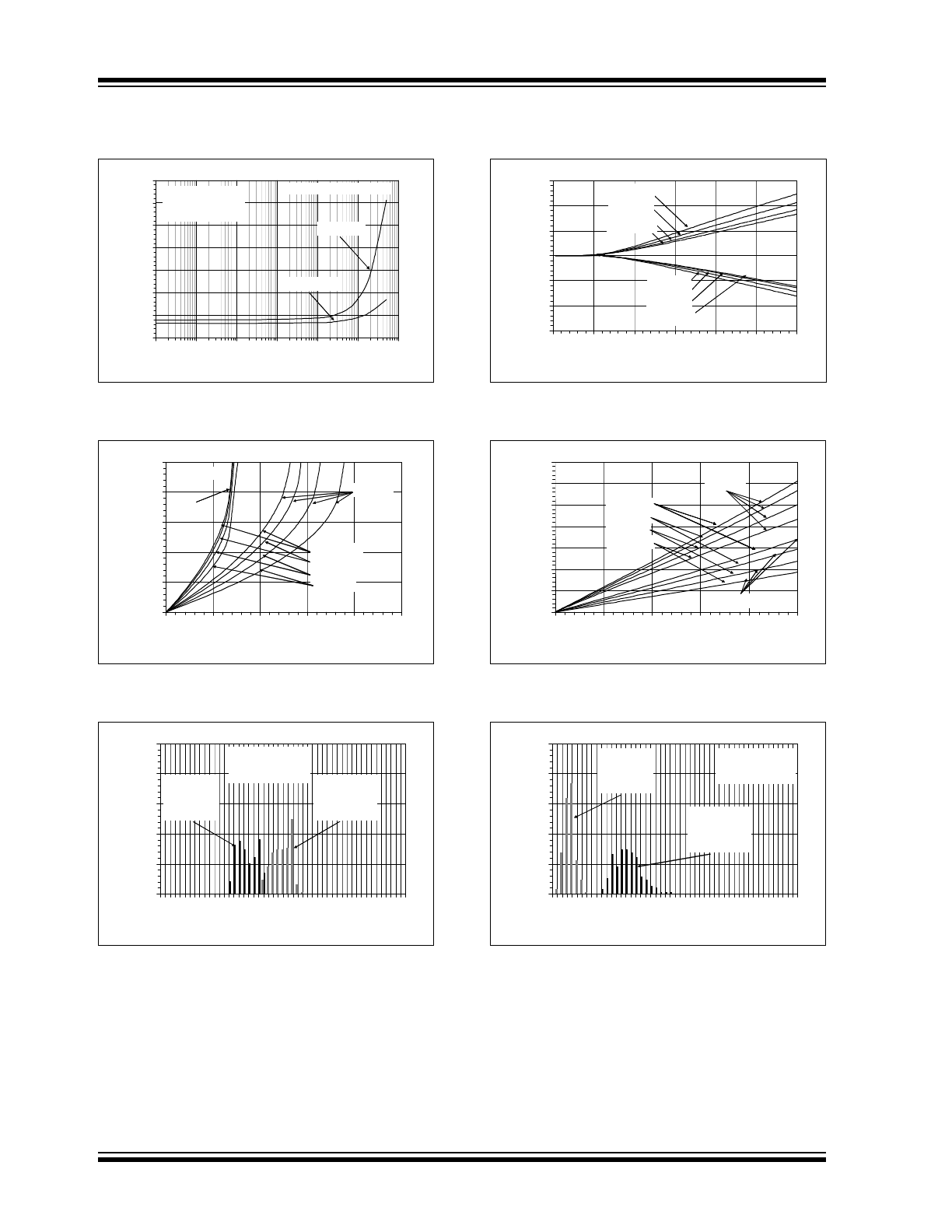
FIGURE 2-19:
Quiescent Current vs.
Toggle Frequency.
FIGURE 2-20:
Output Headroom vs.
Output Current.
FIGURE 2-21:
Low-to-High and High-to-
Low Propagation Delays.
FIGURE 2-22:
Short Circuit Current vs.
Supply Voltage vs. Temperature.
FIGURE 2-23:
Output Headroom vs.Output
Current.
FIGURE 2-24:
Low-to-High and High-to-
Low Propagation Delays .
50
100
150
200
250
300
350
400
10
100
1000
10000 100000 100000
0
1E+07
Toggle Frequency (Hz)
I
Q
(µ
A
)
V
DD
= 1.8V
V
DD
= 5.5V
10
100
1k
10k
100k
1M
10M
100 mV Over-Drive
V
CM
= V
DD
/2
R
L
= Open
0dB Output Attenuation
0
200
400
600
800
1000
0.0
3.0
6.0
9.0
12.0
15.0
I
OUT
(mA)
V
OL
, V
DD
- V
OH
(mV
)
V
DD
= 1.8V
T
A
= +125°C
T
A
= +85°C
T
A
= +25°C
T
A
= -40°C
V
OL
V
OL
V
DD
- V
OH
0%
10%
20%
30%
40%
50%
30
35
40
45
50
55
60
65
70
75
80
Prop. Delay (ns)
O
ccu
rr
en
c
es (
%
)
V
DD
= 1.8V
100 mV Over-Drive
V
CM
= V
DD
/2
t
PLH
Avg. = 47 ns
StDev= 2 ns
198 units
t
PHL
Avg. = 54.4 ns
StDev= 2 ns
198 units
-120
-80
-40
0
40
80
120
0.0
1.0
2.0
3.0
4.0
5.0
6.0
V
DD
(V)
I
SC
(m
A
)
T
A
= -40°C
T
A
= +85°C
T
A
= +125°C
T
A
= +25°C
T
A
= -40°C
T
A
= +125°C
T
A
= +85°C
T
A
= +25°C
0
200
400
600
800
1000
1200
1400
0
5
10
15
20
25
I
OUT
(mA)
V
OL
, V
DD
- V
OH
(mV
)
V
DD
= 5.5V
T
A
= 125°C
T
A
= 85°C
T
A
= -40°C
T
A
= 125°C
T
A
= 25°C
T
A
= 125°C
V
OL
V
DD
- V
OH
0%
10%
20%
30%
40%
50%
30
35
40
45
50
55
60
65
70
75
80
Prop. Delay (ns)
O
ccu
rr
en
c
es (
%
)
V
DD
= 5.5V
100mV Over-Drive
V
CM
= V
DD
/2
t
PLH
Avg. = 44.6 ns
StDev= 2.7 ns
198 units
t
PHL
Avg. = 33 ns
StDev= 1 ns
198 units
2009-2013 Microchip Technology Inc.
DS22139C-page 9
MCP6561/1R/1U/2/4
Note: Unless otherwise indicated, V
DD
= +1.8V to +5.5V, V
SS
= GND, T
A
= +25°C, V
IN
+ = V
DD
/2, V
IN
–
= GND,
R
L
= 10 k
to V
DD
/2, and C
L
= 25 pF.
FIGURE 2-25:
Propagation Delay Skew.
FIGURE 2-26:
Propagation Delay vs.
Supply Voltage.
FIGURE 2-27:
Propagation Delay vs.
Common-mode Input Voltage.
FIGURE 2-28:
Propagation Delay vs.
Temperature.
FIGURE 2-29:
Propagation Delay vs. Input
Over-Drive.
FIGURE 2-30:
Propagation Delay vs.
Common-mode Input Voltage.
0%
10%
20%
30%
40%
50%
-20
-15
-10
-5
0
5
10
15
20
Prop. Delay Skew (ns)
O
ccu
rr
e
n
ces (
%
)
V
DD
= 1.8V
Avg. = -7.3 ns
StDev= 0.8 ns
198 units
V
DD
= 5.5V
Avg. = 11.6 ns
StDev= 2 ns
198 units
100 mV Over-Drive
V
CM
= V
DD
/2
20
40
60
80
100
120
140
1.5
2.5
3.5
4.5
5.5
V
DD
(V)
Prop
. D
e
la
y
(
n
s
)
t
PHL
, 10 mV Over-Drive
t
PLH
, 10 mV Over-Drive
t
PHL
, 100 mV Over-Drive
t
PLH
, 100 mV Over-Drive
V
CM
= V
DD
/2
20
30
40
50
60
70
80
0.00
0.50
1.00
1.50
2.00
V
CM
(V)
Prop
. D
e
la
y
(
n
s
)
t
PLH
t
PHL
V
DD
= 1.8V
100 mV Over-Drive
20
30
40
50
60
70
80
-50
-25
0
25
50
75
100
125
Temperature
(°C)
P
rop.
D
e
la
y
(
n
s
)
t
PHL
t
PLH
, V
DD
= 1.8V
t
PHL
, V
DD
= 1.8V
100 mV Over-Drive
V
CM
= V
DD
/2
t
PLH
, V
DD
= 5.5V
t
PHL
, V
DD
= 5.5V
10
60
110
160
210
260
1
10
100
1000
Over-Drive (mV)
P
rop.
D
e
la
y
(
n
s
)
t
PLH
, V
DD
= 1.8V
t
PHL
, V
DD
= 1.8V
t
PLH
, V
DD
= 5.5V
t
PHL
, V
DD
= 5.5V
V
CM
= V
DD
/2
20
30
40
50
60
70
80
0.0
1.0
2.0
3.0
4.0
5.0
6.0
V
CM
(V)
P
rop.
D
e
la
y
(
n
s
)
t
PLH
t
PHL
V
DD
= 5.5V
100 mV Over-Drive
MCP6561/1R/1U/2/4
DS22139C-page 10
2009-2013 Microchip Technology Inc.
Note: Unless otherwise indicated, V
DD
= +1.8V to +5.5V, V
SS
= GND, T
A
= +25°C, V
IN
+ = V
DD
/2, V
IN
–
= GND,
R
L
= 10 k
to V
DD
/2, and C
L
= 25 pF.
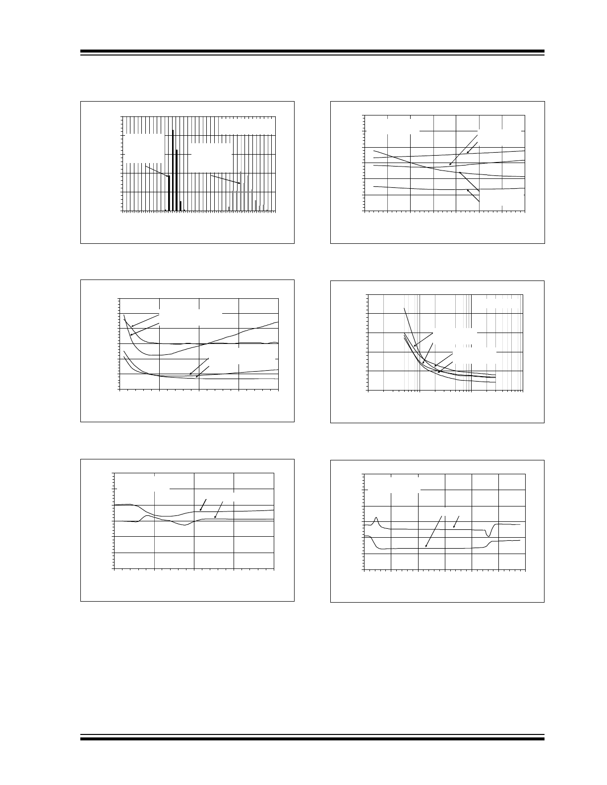
FIGURE 2-31:
Propagation Delay vs.
Capacitive Load.
FIGURE 2-32:
Input Bias Current vs. Input
Voltage vs Temperature.
FIGURE 2-33:
Common-mode Rejection
Ratio and Power Supply Rejection Ratio vs.
Temperature.
FIGURE 2-34:
Power Supply Rejection
Ratio (PSRR).
FIGURE 2-35:
Common-mode Rejection
Ratio (CMRR).
FIGURE 2-36:
Common-mode Rejection
Ratio (CMRR).
0.01
0.1
1
10
100
1000
1
10
100
1000
10000 100000 1E+06
Capacitive Load (nf)
P
rop.
D
e
la
y
(
µ
s
)
0.001
0.01
0.1
1
10
10
1000
V
DD
= 1.8V, t
PLH
V
DD
= 1.8V, t
PHL
V
DD
= 1.8V, t
PLH
V
DD
= 1.8V, t
PHL
V
DD
= 1.8V, t
PLH
V
DD
= 1.8V, t
PHL
V
DD
= 5.5V, t
PLH
V
DD
= 5.5V, t
PHL
100mV Over-Drive
V
CM
= V
DD
/2
1E-01
1E+01
1E+03
1E+05
1E+07
1E+09
1E+11
-0.8
-0.6
-0.4
-0.2
0
Input Voltage
(V)
Inp
u
t C
u
rr
e
n
t
(A
)
T
A
= -40°C
T
A
= +85°C
T
A
= +125°C
T
A
= +25°C
0.1p
10p
1n
100n
10µ
1m
10m
70
72
74
76
78
80
-50
-25
0
25
50
75
100
125
Temperature
(°C)
CM
RR
/P
S
R
R
(
d
B)
V
CM
= -0.3V to V
DD
+ 0.3V
V
DD
= 5.5V
CMRR
V
CM
= V
SS
V
DD
= 1.8V to 5.5V
PSRR
Input Referred
0%
5%
10%
15%
20%
25%
30%
-600
-400
-200
0
200
400
600
PSRR (µV/V)
O
ccu
rr
e
n
ces (
%
)
V
CM
= V
SS
Avg. = 200 µV/V
StDev= 94 µV/V
3588 units
0%
10%
20%
30%
-5
-4
-3
-2
-1
0
1
2
3
4
5
CMRR (mV/V)
O
ccu
rr
e
n
ces (
%
)
V
DD
= 1.8V
3588 units
V
CM
= -0.2V to V
DD
/2
Avg. = 0.5 mV
StDev= 0.1 mV
V
CM
= V
DD
/2 to V
DD
+ 0.2V
Avg. = 0.7 mV
StDev= 1 mV
V
CM
= -0.2V to V
DD
+ 0.2V
Avg. = 0.6 mV
StDev= 0.1 mV
0%
10%
20%
30%
-2.5 -2.0 -1.5 -1.0 -0.5 0.0 0.5 1.0 1.5 2.0 2.5
CMRR (mV/V)
O
ccu
rr
e
n
ces (
%
)
V
DD
= 5.5V
3588 units
V
CM
= -0.3V to V
DD
/2
Avg. = 0.2 mV
StDev= 0.4 mV
V
CM
= V
DD
/2 to V
DD
+ 0.3V
Avg. = 0.03 mV
StDev= 0.7 mV
V
CM
= -0.3V to V
DD
+ 0.3V
Avg. = 0.1 mV
StDev= 0.4 mV