
© 2002-2011 Microchip Technology Inc.
DS21696H-page 1
MCP6541/1R/1U/2/3/4
Features:
• Low Quiescent Current: 600 nA/Comparator (typ.)
• Rail-to-Rail Input: V
SS
- 0.3V to V
DD
+ 0.3V
• CMOS/TTL-Compatible Output
• Propagation Delay: 4 µs
(typical, 100 mV Overdrive)
• Wide Supply Voltage Range: 1.6V to 5.5V
• Available in Single, Dual and Quad
• Single Available in SOT-23-5, SC-70-5 * Packages
• Chip Select (CS) with MCP6543
• Low Switching Current
• Internal Hysteresis: 3.3 mV (typ.)
• Temperature Ranges:
- Industrial: -40°C to +85°C
- Extended: -40°C to +125°C
Typical Applications:
• Laptop Computers
• Mobile Phones
• Metering Systems
• Hand-held Electronics
• RC Timers
• Alarm and Monitoring Circuits
• Windowed Comparators
• Multivibrators
Related Devices:
• Open-Drain Output: MCP6546/7/8/9
Description:
The Microchip Technology Inc. MCP6541/1R/1U/2/3/4
family of comparators is offered in single (MCP6541,
MCP6541R, MCP6541U), single with Chip Select (CS)
(MCP6543), dual (MCP6542) and quad (MCP6544)
configurations. The outputs are push-pull (CMOS/TTL-
compatible) and are capable of driving heavy DC or
capacitive loads.
These comparators are optimized for low-power,
single-supply operation with greater than rail-to-rail
input operation. The push-pull output of the
MCP6541/1R/1U/2/3/4 family supports rail-to-rail out-
put swing and interfaces with TTL/CMOS logic. The
internal input hysteresis eliminates output switching
due to internal input noise voltage, reducing current
draw. The output limits supply current surges and
dynamic power consumption while switching. This
product family operates with a single-supply voltage as
low as 1.6V and draws less than 1 µA/comparator of
quiescent current.
The related MCP6546/7/8/9 family of comparators from
Microchip has an open-drain output. Used with a pull-
up resistor, these devices can be used as level-shifters
for any desired voltage up to 10V and in wired-OR
logic.
* SC-70-5 E-Temp parts not available at this release of
the data sheet.
MCP6541U SOT-23-5 is E-Temp only.
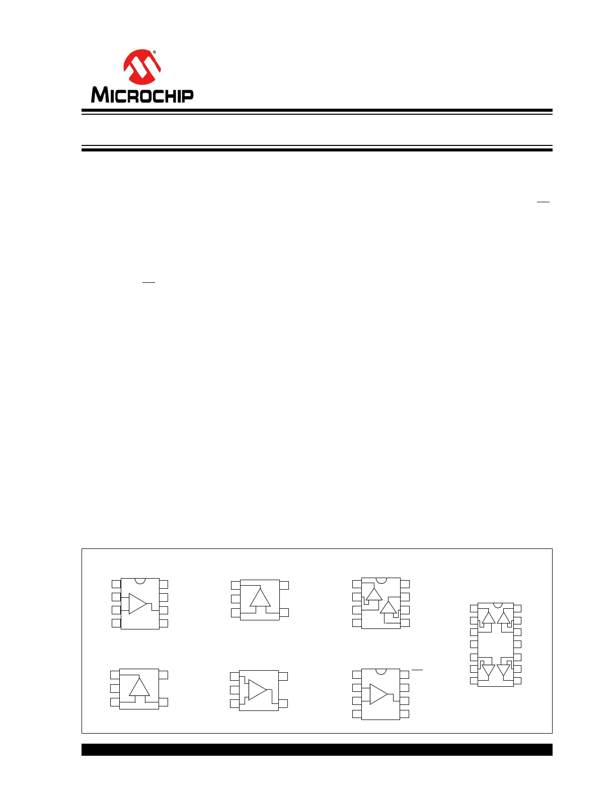
Package Types
V
INA
+
V
IN
–
MCP6541
V
SS
V
DD
OUT
1
2
3
4
8
7
6
5
-
+
NC
NC
NC
PDIP, SOIC, MSOP
4
1
2
3
-
+
5
SOT-23-5
V
DD
OUT
V
IN
+
V
SS
V
IN
–
MCP6542
V
INA
+
V
INA
–
V
SS
1
2
3
4
8
7
6
5
-
OUTA
+ -
+
V
DD
OUTB
V
INB
–
V
INB
+
V
IN
+
V
IN
–
MCP6543
V
SS
V
DD
OUT
1
2
3
4
8
7
6
5
-
+
NC
CS
NC
PDIP, SOIC, MSOP
PDIP, SOIC, MSOP
MCP6544
V
INA
+
V
INA
–
V
SS
1
2
3
4
14
13
12
11
-
OUTA
+ -
+
V
DD
OUTD
V
IND
–
V
IND
+
10
9
8
5
6
7
OUTB
V
INB
–
V
INB
+
V
INC
+
V
INC
-
OUTC
+
-
-
+
PDIP, SOIC, TSSOP
-
+
MCP6541R
4
1
2
3
5
SC-70-5, SOT-23-5
V
SS
V
IN
+
V
IN
–
V
DD
OUT
MCP6541U
-
+
4
1
2
3
-
+
5
V
SS
OUT
V
IN
+
V
DD
V
IN
–
MCP6541
SC-70-5, SOT-23-5
Push-Pull Output Sub-Microamp Comparators

MCP6541/1R/1U/2/3/4
DS21696H-page 2
© 2002-2011 Microchip Technology Inc.
NOTES:
© 2002-2011 Microchip Technology Inc.
DS21696H-page 3
MCP6541/1R/1U/2/3/4
1.0
ELECTRICAL
CHARACTERISTICS
Absolute Maximum Ratings †
V
DD
- V
SS
.........................................................................7.0V
Current at Analog Input Pin (V
IN
+, V
IN
-.........................±2 mA
Analog Input (V
IN
) †† ...................... V
SS
- 1.0V to V
DD
+ 1.0V
All other Inputs and Outputs........... V
SS
- 0.3V to V
DD
+ 0.3V
Difference Input Voltage ....................................... |V
DD
- V
SS
|
Output Short-Circuit Current ................................ Continuous
Current at Input Pins ....................................................±2 mA
Current at Output and Supply Pins ............................±30 mA
Storage Temperature ....................................-65°C to +150°C
Maximum Junction Temperature (T
J
) .......................... +150°C
ESD Protection on all Pins (HBM;MM) ..................4 kV; 400V
† Notice: Stresses above those listed under “Absolute
Maximum Ratings” may cause permanent damage to the
device. This is a stress rating only and functional operation of
the device at those or any other conditions above those
indicated in the operational listings of this specification is not
implied. Exposure to maximum rating conditions for extended
periods may affect device reliability.
†† See
Section 4.1.2 “Input Voltage and Current
Limits”
DC CHARACTERISTICS
Electrical Specifications: Unless otherwise indicated, V
DD
= +1.6V to +5.5V, V
SS
= GND, T
A
= +25°C,V
IN
+ = V
DD
/2,
V
IN
–
= V
SS
, and R
L
= 100 k
Ω to V
DD
/2 (Refer to
Figure 1-3
).
Parameters
Sym
Min
Typ
Max
Units
Conditions
Power Supply
Supply Voltage
V
DD
1.6
—
5.5
V
Quiescent Current per comparator
I
Q
0.3
0.6
1.0
µA
I
OUT
= 0
Input
Input Voltage Range
V
CMR
V
SS
−0.3
—
V
DD
+0.3
V
Common Mode Rejection Ratio
CMRR
55
70
—
dB
V
DD
= 5V, V
CM
= -0.3V to 5.3V
Common Mode Rejection Ratio
CMRR
50
65
—
dB
V
DD
= 5V, V
CM
= 2.5V to 5.3V
Common Mode Rejection Ratio
CMRR
55
70
—
dB
V
DD
= 5V, V
CM
= -0.3V to 2.5V
Power Supply Rejection Ratio
PSRR
63
80
—
dB
V
CM
= V
SS
Input Offset Voltage
V
OS
-7.0
±1.5
+7.0
mV
V
CM
= V
SS
(
Note 1
)
Drift with Temperature
ΔV
OS
/
ΔT
A
—
±3
—
µV/°C
T
A
= -40°C to +125°C, V
CM
= V
SS
Input Hysteresis Voltage
V
HYST
1.5
3.3
6.5
mV
V
CM
= V
SS
(
Note 1
)
Linear Temp. Co. (
Note 2
)
TC
1
—
6.7
—
µV/°C
T
A
= -40°C to +125°C, V
CM
= V
SS
Quadratic Temp. Co. (
Note 2
)
TC
2
—
-0.035
—
µV/°C
2
T
A
= -40°C to +125°C, V
CM
= V
SS
Input Bias Current
I
B
—
1
—
pA
V
CM
=
V
SS
At Temperature (I-Temp parts)
I
B
—
25
100
pA
T
A
= +85°C, V
CM
= V
SS
(
Note 3
)
At Temperature (E-Temp parts)
I
B
—
1200
5000
pA
T
A
= +125°C, V
CM
= V
SS
(
Note 3
)
Input Offset Current
I
OS
—
±1
—
pA
V
CM
=
V
SS
Common Mode Input Impedance
Z
CM
—
10
13
||4
—
Ω||pF
Differential Input Impedance
Z
DIFF
—
10
13
||2
—
Ω||pF
Note
1:
The input offset voltage is the center (average) of the input-referred trip points. The input hysteresis is the difference
between the input-referred trip points.
2:
V
HYST
at different temperatures is estimated using V
HYST
(T
A
) = V
HYST
+ (T
A
- 25°C) TC
1
+ (T
A
- 25°C)
2
TC
2
.
3:
Input bias current at temperature is not tested for SC-70-5 package.
4:
Limit the output current to Absolute Maximum Rating of 30 mA.
MCP6541/1R/1U/2/3/4
DS21696H-page 4
© 2002-2011 Microchip Technology Inc.
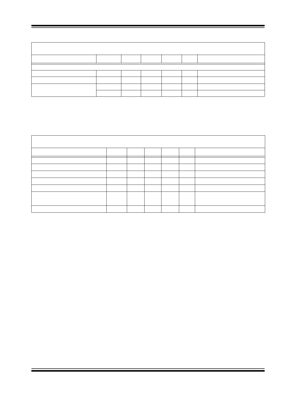
AC CHARACTERISTICS
Push-Pull Output
High-Level Output Voltage
V
OH
V
DD
−0.2
—
—
V
I
OUT
= -2 mA, V
DD
= 5V
Low-Level Output Voltage
V
OL
—
—
V
SS
+0.2
V
I
OUT
= 2 mA, V
DD
= 5V
Short-Circuit Current
I
SC
—
-2.5, +1.5
—
mA
V
DD
= 1.6V (
Note 4
)
I
SC
—
±30
—
mA
V
DD
= 5.5V (
Note 4
)
Electrical Specifications: Unless otherwise indicated, V
DD
= +1.6V to +5.5V, V
SS
= GND, T
A
= +25°C,
V
IN
+ = V
DD
/2, Step = 200 mV, Overdrive = 100 mV, and C
L
= 36 pF (Refer to
Figure 1-2
and
Figure 1-3
).
Parameters
Sym
Min
Typ
Max
Units
Conditions
Rise Time
t
R
—
0.85
—
µs
Fall Time
t
F
—
0.85
—
µs
Propagation Delay (High-to-Low)
t
PHL
—
4
8
µs
Propagation Delay (Low-to-High)
t
PLH
—
4
8
µs
Propagation Delay Skew
t
PDS
—
±0.2
—
µs
(
Note 1
)
Maximum Toggle Frequency
f
MAX
—
160
—
kHz
V
DD
= 1.6V
f
MAX
—
120
—
kHz
V
DD
= 5.5V
Input Noise Voltage
E
ni
—
200
—
µV
P-P
10 Hz to 100 kHz
Note 1:
Propagation Delay Skew is defined as: t
PDS
= t
PLH
- t
PHL
.
DC CHARACTERISTICS (CONTINUED)
Electrical Specifications: Unless otherwise indicated, V
DD
= +1.6V to +5.5V, V
SS
= GND, T
A
= +25°C,V
IN
+ = V
DD
/2,
V
IN
–
= V
SS
, and R
L
= 100 k
Ω to V
DD
/2 (Refer to
Figure 1-3
).
Parameters
Sym
Min
Typ
Max
Units
Conditions
Note
1:
The input offset voltage is the center (average) of the input-referred trip points. The input hysteresis is the difference
between the input-referred trip points.
2:
V
HYST
at different temperatures is estimated using V
HYST
(T
A
) = V
HYST
+ (T
A
- 25°C) TC
1
+ (T
A
- 25°C)
2
TC
2
.
3:
Input bias current at temperature is not tested for SC-70-5 package.
4:
Limit the output current to Absolute Maximum Rating of 30 mA.
© 2002-2011 Microchip Technology Inc.
DS21696H-page 5
MCP6541/1R/1U/2/3/4
FIGURE 1-1:
Timing Diagram for the CS
Pin on the MCP6543.
FIGURE 1-2:
Propagation Delay Timing
Diagram.
MCP6543 CHIP SELECT (CS) CHARACTERISTICS
Electrical Specifications: Unless otherwise indicated, V
DD
= +1.6V to +5.5V, V
SS
= GND, T
A
= +25°C, V
IN
+ =
V
DD
/2, V
IN
– = V
SS
, and C
L
= 36 pF (Refer to Figures
1-1
and
1-3
).
Parameters
Sym
Min
Typ
Max
Units
Conditions
CS Low Specifications
CS Logic Threshold, Low
V
IL
V
SS
—
0.2 V
DD
V
CS Input Current, Low
I
CSL
—
5.0
—
pA
CS = V
SS
CS High Specifications
CS Logic Threshold, High
V
IH
0.8 V
D
D
—
V
DD
V
CS Input Current, High
I
CSH
—
1
—
pA
CS = V
DD
CS Input High, V
DD
Current
I
DD
—
18
—
pA
CS = V
DD
CS Input High, GND Current
I
SS
—
–20
—
pA
CS = V
DD
Comparator Output Leakage
I
O(LEAK)
—
1
—
pA
V
OUT
= V
DD
,
CS = V
DD
CS Dynamic Specifications
CS Low to Comparator Output
Low Turn-on Time
t
ON
—
2
50
ms
CS = 0.2 V
DD
to V
OUT
= V
DD
/2,
V
IN
– = V
DD
CS High to Comparator Output
High Z Turn-off Time
t
OFF
—
10
—
µs
CS = 0.8 V
DD
to V
OUT
= V
DD
/2,
V
IN
– = V
DD
CS Hysteresis
V
CS_HYS
T
—
0.6
—
V
V
DD
= 5V
V
IL
Hi-Z
t
ON
V
IH
CS
t
OFF
V
OUT
-20 pA (typ.)
Hi-Z
I
SS
I
CS
1 pA (typ.)
1 pA (typ.)
-20 pA (typ.)
-0.6 µA (typ.)
V
OL
t
PLH
V
OUT
V
IN
–
100 mV
100 mV
t
PHL
V
OL
V
IN
+ = V
DD
/2
V
OH
MCP6541/1R/1U/2/3/4
DS21696H-page 6
© 2002-2011 Microchip Technology Inc.
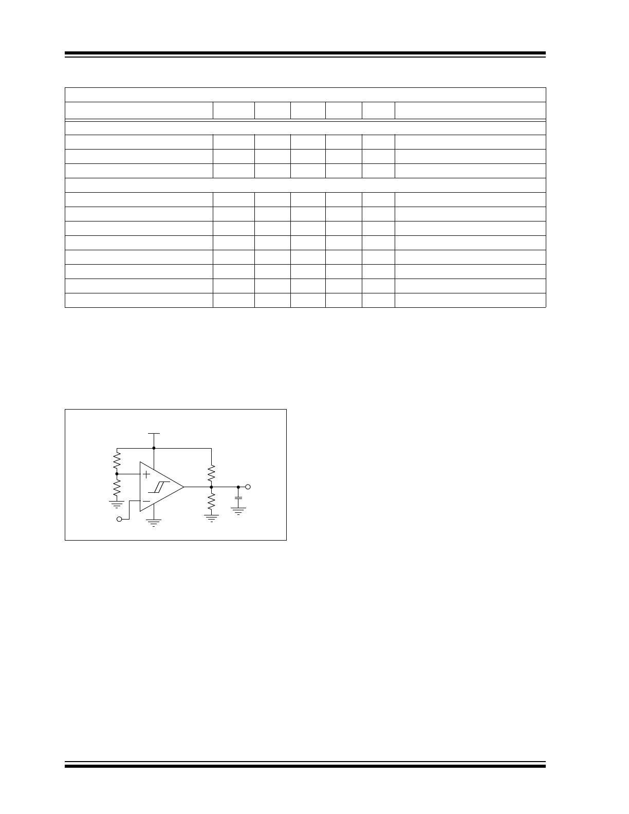
TEMPERATURE CHARACTERISTICS
1.1
Test Circuit Configuration
This test circuit configuration is used to determine the
AC and DC specifications.
FIGURE 1-3:
AC and DC Test Circuit for
the Push-Pull Output Comparators.
Electrical Specifications: Unless otherwise indicated, V
DD
= +1.6V to +5.5V and V
SS
= GND.
Parameters
Sym
Min
Typ
Max
Units
Conditions
Temperature Ranges
Specified Temperature Range
T
A
-40
—
+85
°C
Operating Temperature Range
T
A
-40
—
+125
°C
Note
Storage Temperature Range
T
A
-65
—
+150
°C
Thermal Package Resistances
Thermal Resistance, 5L-SC-70
θ
JA
—
331
—
°C/W
Thermal Resistance, 5L-SOT-23
θ
JA
—
220.7
—
°C/W
Thermal Resistance, 8L-PDIP
θ
JA
—
89.3
—
°C/W
Thermal Resistance, 8L-SOIC
θ
JA
—
149.5
—
°C/W
Thermal Resistance, 8L-MSOP
θ
JA
—
211
—
°C/W
Thermal Resistance, 14L-PDIP
θ
JA
—
70
—
°C/W
Thermal Resistance, 14L-SOIC
θ
JA
—
95.3
—
°C/W
Thermal Resistance, 14L-TSSOP
θ
JA
—
100
—
°C/W
Note:
The MCP6541/1R/1U/2/3/4 I-Temp parts operate over this extended temperature range, but with reduced
performance. In any case, the Junction Temperature (T
J
) must not exceed the Absolute Maximum
specification of +150°C.
V
DD
V
SS
= 0V
200 k
Ω
200 k
Ω
200 k
Ω
200 k
Ω
V
OUT
V
IN
= V
SS
36 pF
MCP654X
© 2002-2011 Microchip Technology Inc.
DS21696H-page 7
MCP6541/1R/1U/2/3/4
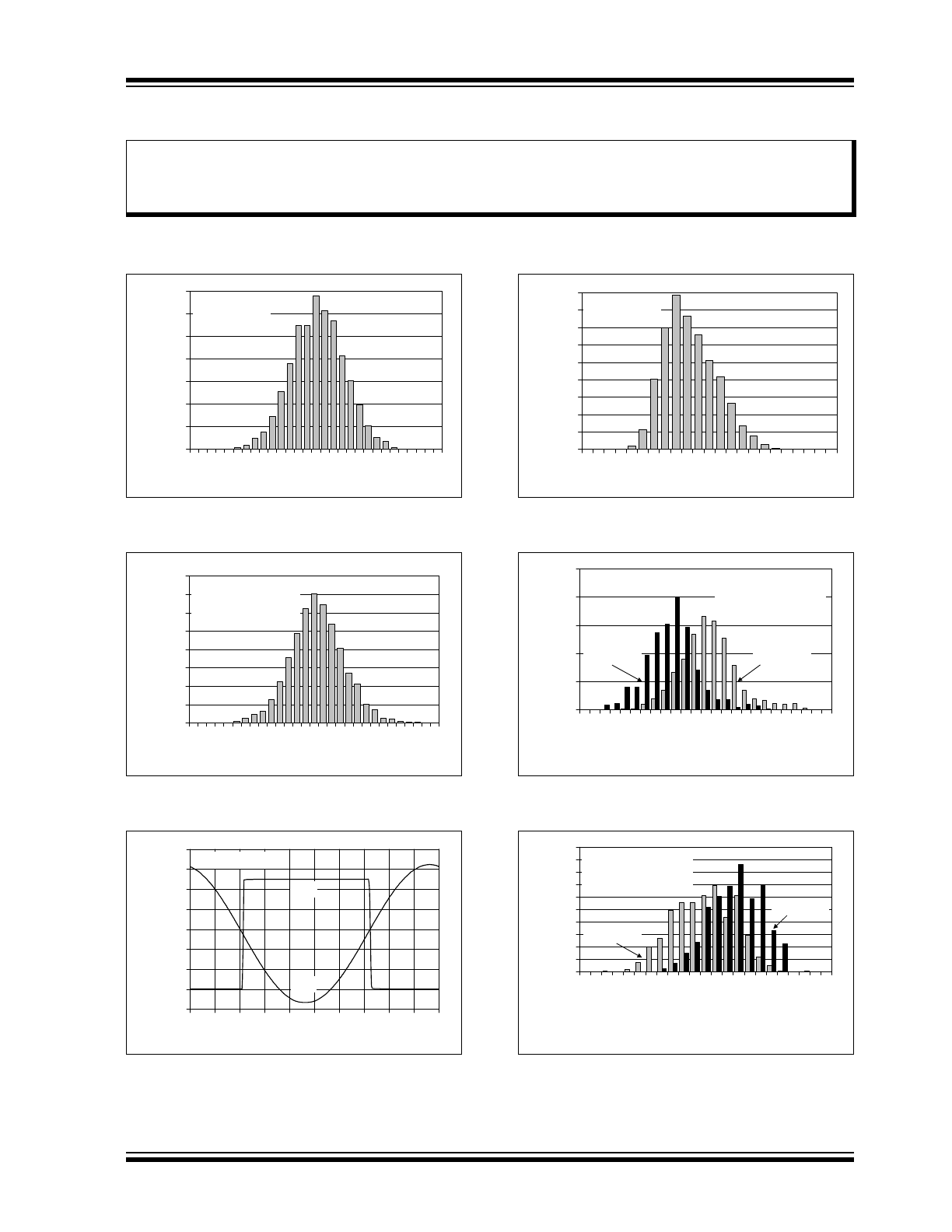
2.0
TYPICAL PERFORMANCE CURVES
Note: Unless otherwise indicated, V
DD
= +1.6V to +5.5V, V
SS
= GND, T
A
= +25°C, V
IN
+ = V
DD
/2, V
IN
–
= GND,
R
L
= 100 k
Ω to V
DD
/2, and C
L
= 36 pF.
FIGURE 2-1:
Input Offset Voltage at
V
CM
= V
SS
.
FIGURE 2-2:
Input Offset Voltage Drift at
V
CM
= V
SS
.
FIGURE 2-3:
The MCP6541/1R/1U/2/3/4
Comparators Show No Phase Reversal.
FIGURE 2-4:
Input Hysteresis Voltage at
V
CM
= V
SS
.
FIGURE 2-5:
Input Hysteresis Voltage
Linear Temp. Co. (TC
1
) at V
CM
= V
SS
.
FIGURE 2-6:
Input Hysteresis Voltage
Quadratic Temp. Co. (TC
2
) at V
CM
= V
SS
.
Note:
The graphs and tables provided following this note are a statistical summary based on a limited number of
samples and are provided for informational purposes only. The performance characteristics listed herein
are not tested or guaranteed. In some graphs or tables, the data presented may be outside the specified
operating range (e.g., outside specified power supply range) and therefore outside the warranted range.
0%
2%
4%
6%
8%
10%
12%
14%
-7 -6 -5 -4 -3 -2 -1 0
1
2
3
4
5
6
7
Input Offset Voltage (mV)
P
e
rcentage of Occurrences
1200 Samples
V
CM
= V
SS
0%
2%
4%
6%
8%
10%
12%
14%
16%
-1
4
-1
2
-1
0
-8
-6
-4
-2
0
2
4
6
8
10
12
14
Input Offset Voltage Drift (µV/°C)
P
e
rcent
a
ge
of
Occ
u
rr
en
ces
1200 Samples
V
CM
= V
SS
T
A
= -40°C to +125°C
-1
0
1
2
3
4
5
6
7
0
1
2
3
4
5
6
7
8
9
10
Time (1 ms/div)
In
vert
ing I
nput
, Out
put
V
o
lt
age
(V
)
V
OUT
V
IN
–
V
DD
= 5.5V
0%
2%
4%
6%
8%
10%
12%
14%
16%
18%
1.6 2.0 2.4 2.8 3.2 3.6 4.0 4.4 4.8 5.2 5.6 6.0
Input Hysteresis Voltage (mV)
P
e
rcentage of Occurrences
1200 Samples
V
CM
= V
SS
0%
5%
10%
15%
20%
25%
4.
6
5.
0
5.
4
5.
8
6.
2
6.
6
7.
0
7.
4
7.
8
8.
2
8.
6
9.
0
9.
4
Input Hysteresis Voltage –
Linear Temp. Co.; TC
1
(µV/°C)
P
e
rcentage of Occurrences
596 Samples
V
CM
= V
SS
T
A
= -40°C to +125°C
V
DD
= 1.6V
V
DD
= 5.5V
0%
2%
4%
6%
8%
10%
12%
14%
16%
18%
20%
-0.
060
-0.
056
-0.
052
-0.
048
-0.
044
-0.
040
-0.
036
-0.
032
-0.
028
-0.
024
-0.
020
-0.
016
Input Hysteresis Voltage –
Quadratic Temp. Co.; TC
2
(µV/°C
2
)
P
e
rcentage of Occurrences
596 Samples
V
CM
= V
SS
T
A
= -40°C to +125°C
V
DD
= 5.5V
V
DD
= 1.6V
MCP6541/1R/1U/2/3/4
DS21696H-page 8
© 2002-2011 Microchip Technology Inc.
Note: Unless otherwise indicated, V
DD
= +1.6V to +5.5V, V
SS
= GND, T
A
= +25°C, V
IN
+ = V
DD
/2, V
IN
– = GND,
R
L
= 100 k
Ω to V
DD
/2, and C
L
= 36 pF.
FIGURE 2-7:
Input Offset Voltage vs.
Ambient Temperature at V
CM
= V
SS
.
FIGURE 2-8:
Input Offset Voltage vs.
Common Mode Input Voltage at V
DD
= 1.6V.
FIGURE 2-9:
Input Offset Voltage vs.
Common Mode Input Voltage at V
DD
= 5.5V.
FIGURE 2-10:
Input Hysteresis Voltage vs.
Ambient Temperature at V
CM
= V
SS
.
FIGURE 2-11:
Input Hysteresis Voltage vs.
Common Mode Input Voltage at V
DD
= 1.6V.
FIGURE 2-12:
Input Hysteresis Voltage vs.
Common Mode Input Voltage at V
DD
= 5.5V.
-1.0
-0.8
-0.6
-0.4
-0.2
0.0
0.2
0.4
0.6
0.8
1.0
-50
-25
0
25
50
75
100
125
Ambient Temperature (°C)
In
p
u
t
Off
set
V
o
lta
g
e (
m
V
)
V
DD
= 1.6V
V
DD
= 5.5V
V
CM
= V
SS
-2.0
-1.5
-1.0
-0.5
0.0
0.5
1.0
1.5
2.0
-0.
4
-0.
2
0.
0
0.
2
0.
4
0.
6
0.
8
1.
0
1.
2
1.
4
1.
6
1.
8
2.
0
Common Mode Input Voltage (V)
Input O
ffset Vol
tage (mV)
V
DD
= 1.6V
T
A
= +125°C
T
A
= +85°C
T
A
= +25°C
T
A
= -40°C
T
A
= +125°C
-2.0
-1.5
-1.0
-0.5
0.0
0.5
1.0
1.5
2.0
-0.
5
0.
0
0.
5
1.
0
1.
5
2.
0
2.
5
3.
0
3.
5
4.
0
4.
5
5.
0
5.
5
6.
0
Common Mode Input Voltage (V)
Input O
ffset Vol
tage (mV)
V
DD
= 5.5V
T
A
= +85°C
T
A
= +125°C
T
A
= -40°C
T
A
= +25°C
1.5
2.0
2.5
3.0
3.5
4.0
4.5
5.0
5.5
6.0
6.5
-50
-25
0
25
50
75
100
125
Ambient Temperature (°C)
Input H
ysteresi
s Vol
tage (mV)
V
DD
= 1.6V
V
DD
= 5.5V
V
CM
= V
SS
1.5
2.0
2.5
3.0
3.5
4.0
4.5
5.0
5.5
6.0
-0.
4
-0.
2
0.
0
0.
2
0.
4
0.
6
0.
8
1.
0
1.
2
1.
4
1.
6
1.
8
2.
0
Common Mode Input Voltage (V)
Input H
ysteresi
s Vol
tage (mV)
T
A
= -40°C
T
A
= +125°C
T
A
= +85°C
T
A
= +25°C
V
DD
= 1.6V
1.5
2.0
2.5
3.0
3.5
4.0
4.5
5.0
5.5
6.0
-0.
5
0.
0
0.
5
1.
0
1.
5
2.
0
2.
5
3.
0
3.
5
4.
0
4.
5
5.
0
5.
5
6.
0
Common Mode Input Voltage (V)
Input H
ysteresi
s Vol
tage (mV)
V
DD
= 5.5V
T
A
= +125°C
T
A
= +85°C
T
A
= +25°C
T
A
= -40°C
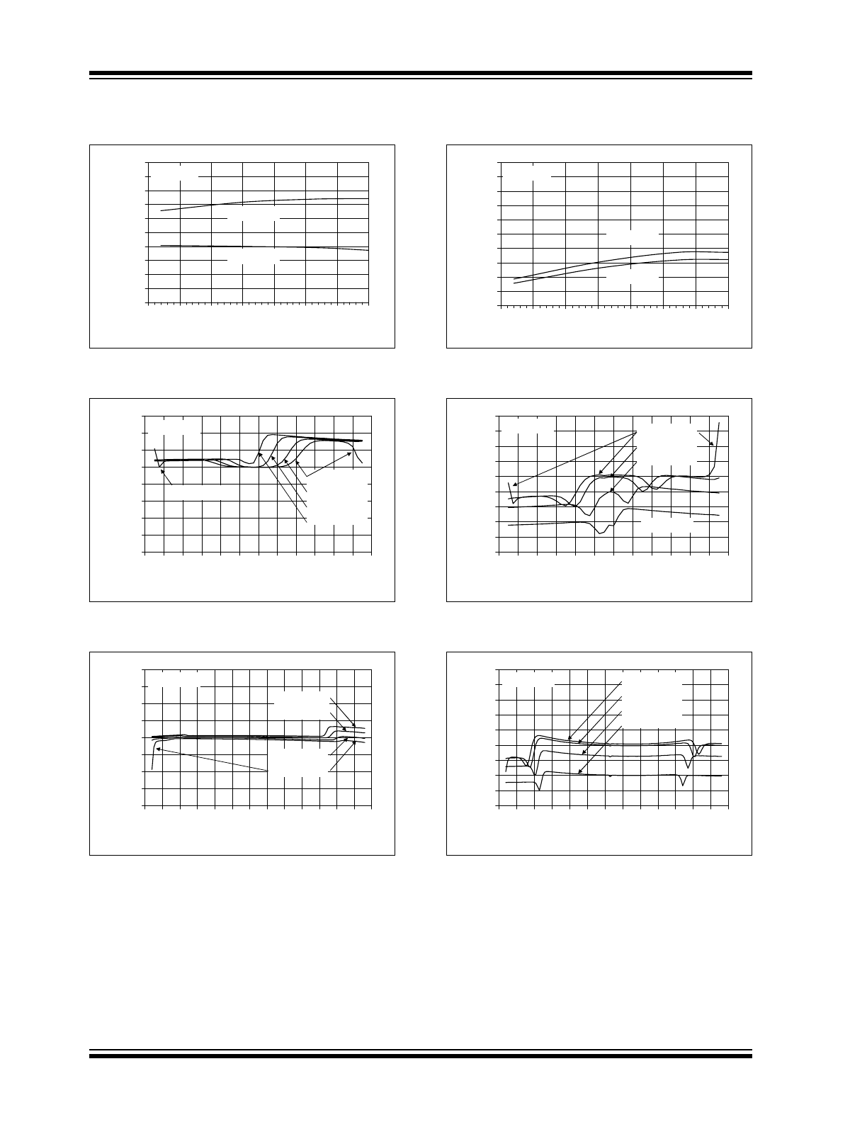
© 2002-2011 Microchip Technology Inc.
DS21696H-page 9
MCP6541/1R/1U/2/3/4
Note: Unless otherwise indicated, V
DD
= +1.6V to +5.5V, V
SS
= GND, T
A
= +25°C, V
IN
+ = V
DD
/2, V
IN
– = GND,
R
L
= 100 k
Ω to V
DD
/2, and C
L
= 36 pF.
FIGURE 2-13:
CMRR, PSRR vs. Ambient
Temperature.
FIGURE 2-14:
Input Bias Current, Input
Offset Current vs. Ambient Temperature.
FIGURE 2-15:
Quiescent Current vs.
Common Mode Input Voltage at V
DD
= 1.6V.
FIGURE 2-16:
Input Bias Current, Input
Offset Current vs. Common Mode Input Voltage.
FIGURE 2-17:
Quiescent Current vs.
Power Supply Voltage.
FIGURE 2-18:
Quiescent Current vs.
Common Mode Input Voltage at V
DD
= 5.5V.
55
60
65
70
75
80
85
90
-50
-25
0
25
50
75
100
125
Ambient Temperature (°C)
CM
RR,
P
S
RR (
d
B)
Input Referred
PSRR, V
IN
+ = V
SS
, V
DD
= 1.6V to 5.5V
CMRR, V
IN
+ = -0.3 to 5.3V, V
DD
= 5.0V
0.1
1
10
100
1000
55
65
75
85
95
105
115
125
Ambient Temperature (°C)
Input B
ias,
O
ffset C
u
rrents
(pA
)
I
B
| I
OS
|
V
DD
= 5.5V
V
CM
= V
DD
0.0
0.1
0.2
0.3
0.4
0.5
0.6
0.7
0.0
0.2
0.4
0.6
0.8
1.0
1.2
1.4
1.6
Common Mode Input Voltage (V)
Qui
escent C
u
rr
e
nt
per
com
p
ar
ator
(µA
)
V
DD
= 1.6V
Sweep V
IN
+, V
IN
– = V
DD
/2
Sweep V
IN
–, V
IN
+ = V
DD
/2
0.1
1
10
100
1000
10000
0.0 0.5 1.0 1.5 2.0 2.5 3.0 3.5 4.0 4.5 5.0 5.5
Common Mode Input Voltage (V)
Input B
ias,
O
ffset C
u
rrents (A
)
V
DD
= 5.5V
100f
100p
1p
10p
1n
10n
I
B
, T
A
= +125°C
I
B
, T
A
= +85°C
I
OS
, T
A
= +125°C
I
OS
, T
A
= +85°C
0.0
0.1
0.2
0.3
0.4
0.5
0.6
0.7
0.0 0.5 1.0 1.5 2.0 2.5 3.0 3.5 4.0 4.5 5.0 5.5
Power Supply Voltage (V)
Qui
escent C
u
rr
e
nt
per
C
o
m
p
ar
ator
(µA
)
T
A
= +125°C
T
A
= +85°C
T
A
= +25°C
T
A
= -40°C
0.0
0.1
0.2
0.3
0.4
0.5
0.6
0.7
0.0 0.5 1.0 1.5 2.0 2.5 3.0 3.5 4.0 4.5 5.0 5.5
Common Mode Input Voltage (V)
Qui
escent C
u
rr
e
nt
per
C
o
m
p
ar
ator
(µA
)
V
DD
= 5.5V
Sweep V
IN
+, V
IN
– = V
DD
/2
Sweep V
IN
–, V
IN
+ = V
DD
/2
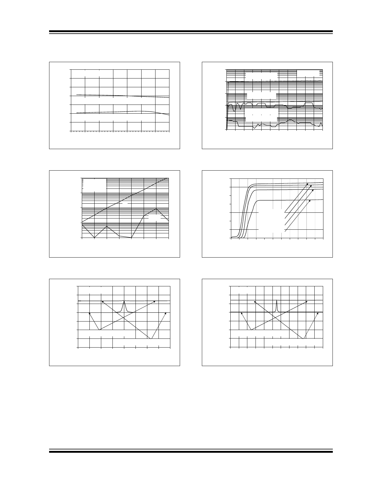
MCP6541/1R/1U/2/3/4
DS21696H-page 10
© 2002-2011 Microchip Technology Inc.
Note: Unless otherwise indicated, V
DD
= +1.6V to +5.5V, V
SS
= GND, T
A
= +25°C, V
IN
+ = V
DD
/2, V
IN
– = GND,
R
L
= 100 k
Ω to V
DD
/2, and C
L
= 36 pF.
FIGURE 2-19:
Supply Current vs. Toggle
Frequency.
FIGURE 2-20:
Output Voltage Headroom
vs. Output Current at V
DD
= 1.6V.
FIGURE 2-21:
High-to-Low Propagation
Delay.
FIGURE 2-22:
Output Short Circuit Current
Magnitude vs. Power Supply Voltage.
FIGURE 2-23:
Output Voltage Headroom
vs. Output Current at V
DD
= 5.5V.
FIGURE 2-24:
Low-to-High Propagation
Delay.
0.1
1
10
0.1
1
10
100
Toggle Frequency (kHz)
Suppl
y C
u
rrent (µA
)
V
DD
= 5.5V
V
DD
= 1.6V
100 mV Overdrive
V
CM
= V
DD
/2
R
L
= infinity
0.0
0.1
0.2
0.3
0.4
0.5
0.6
0.7
0.8
0.0
0.5
1.0
1.5
2.0
2.5
3.0
Output Current (mA)
Output V
o
lt
age H
eadr
oom
(V
)
V
DD
= 1.6V
V
OL
–V
SS
:
T
A
= +125°C
T
A
= +85°C
T
A
= +25°C
T
A
= -40°C
T
A
= +125°C
T
A
= +85°C
T
A
= +25°C
T
A
= -40°C
V
DD
–V
OH
:
0%
5%
10%
15%
20%
25%
30%
35%
40%
45%
0
1
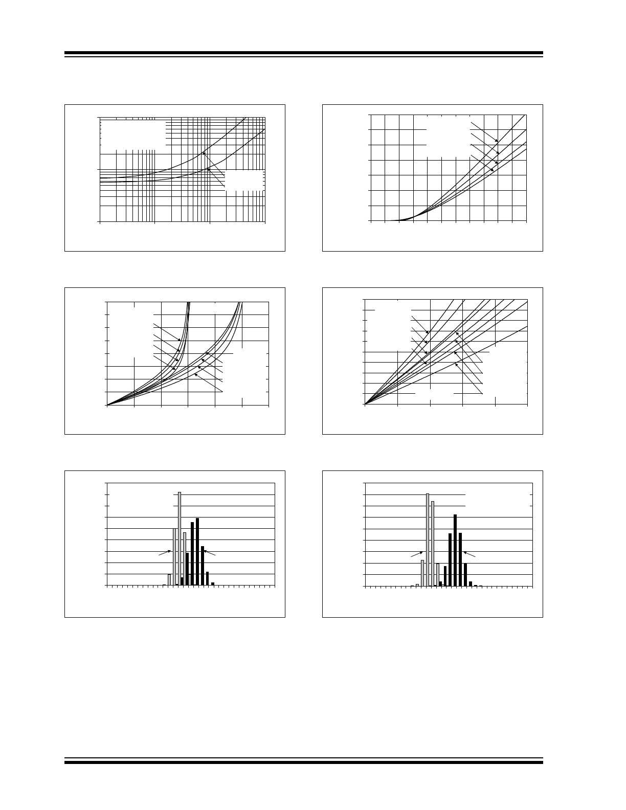
2
3
4
5
6
7
8
High-to-Low Propagation Delay (µs)
P
e
rcentage of Occur
re
nces
600 Samples
100 mV Overdrive
V
CM
= V
DD
/2
V
DD
= 5.5V
V
DD
= 1.6V
0
5
10
15
20
25
30
35
0.0 0.5 1.0 1.5 2.0 2.5 3.0 3.5 4.0 4.5 5.0 5.5
Power Supply Voltage (V)
O
u
tput Short C
ircui
t C
u
rrent
Magni
tude (mA
)
T
A
= -40°C
T
A
= +25°C
T
A
= +85°C
T
A
= +125°C
0.0
0.1
0.2
0.3
0.4
0.5
0.6
0.7
0.8
0.9
1.0
0
5
10
15
20
25
Output Current (mA)
Output V
o
lt
age H
eadr
oom
(V
)
V
DD
= 5.5V
T
A
= +125°C
T
A
= +85°C
T
A
= +25°C
T
A
= -40°C
V
DD
– V
OH
:
T
A
= +125°C
T
A
= +85°C
T
A
= +25°C
T
A
= -40°C
V
OL
– V
SS
:
0%
5%
10%
15%
20%
25%
30%
35%
40%
45%
0
1
2
3
4
5
6
7
8
Low-to-High Propagation Delay (µs)
P
e
rcentage of Occur
re
nces
600 Samples
100 mV Overdrive
V
CM
= V
DD
/2
V
DD
= 5.5V
V
DD
= 1.6V