
2009-2014 Microchip Technology Inc.
DS20002146D-page 1
MCP651/1S/2/3/4/5/9
Features:
• Gain-Bandwidth Product: 50 MHz
• Slew Rate: 30 V/µs
• Low Input Offset: ±200 µV (maximum)
• Low Input Bias Current: 6 pA (typical)
• Noise: 7.5 nV/
Hz, at 1 MHz
• Ease-of-Use:
- Unity-Gain Stable
- Rail-to-Rail Output
- Input Range incl. Negative Rail
- No Phase Reversal
• Supply Voltage Range: +2.5V to +5.5V
• High Output Current: ±100 mA
• Supply Current: 6.0 mA/Ch (typical)
• Low-Power Mode: 5 µA/Ch
• Small Packages: SOT23-5, DFN
• Extended Temperature Range: -40°C to +125°C
Typical Applications:
• Driving A/D Converters
• Fast Low-side Current Sensing
• Power Amplifier Control Loops
• Optical Detector Amplifier
• Barcode Scanners
• Multi-Pole Active Filter
• Consumer Audio
Design Aids:
• SPICE Macro Models
• FilterLab
®
Software
• Microchip Advanced Part Selector (MAPS)
• Analog Demonstration and Evaluation Boards
- MCP651EV-VOS
• Application Notes
Description:
The Microchip Technology Inc. MCP651/1S/2/3/4/5/9
family of high bandwidth and high slew rate operational
amplifiers features low offset. At power-up, these op
amps are self-calibrated using mCal. Some package
options also provide a Calibration/Chip Select pin
(CAL/CS) that supports a Low-Power mode of
operation, with offset calibration at the time normal
operation is re-started. These amplifiers are optimized
for high speed, low noise and distortion, single-supply
operation with rail-to-rail output and an input that
includes the negative rail.
This family is offered in single (MCP651 and
MCP651S), single with CAL/CS pin (MCP653), dual
(MCP652), dual with CAL/CS pins (MCP655), quad
(MCP654) and quad with CAL/CS pins (MCP659). All
devices are fully specified from -40°C to +125°C.
Typical Application Circuit
1 k
100 k
MCP65X
V
IN
V
DD
/2
V
OUT
R
L
High Gain Amplifier (G = 101V/V)
0%
5%
10%
15%
20%
25%
30%
35%
-100 -80 -60 -40 -20
0
20
40
60
80 100
Input Offset Voltage (µV)
P
er
cent
age o
f O
ccur
re
nces
80 Samples
T
A
= +25°C
V
DD
= 2.5V and 5.5V
Calibrated at +25°C
High Gain-Bandwidth Op Amp Portfolio
Model Family
Channels/Package
Gain-Bandwidth
V
OS
(max.)
I
Q
/Ch (typ.)
MCP621/1S/2/3/4/5/9
1, 2, 4
20 MHz
0.2 mV
2.5 mA
MCP631/2/3/4/5/9
1, 2, 4
24 MHz
8.0 mV
2.5 mA
MCP651/1S/2/3/4/5/9
1, 2, 4
50 MHz
0.2 mV
6.0 mA
MCP660/1/2/3/4/5/9
1, 2, 3, 4
60 MHz
8.0 mV
6.0 mA
50 MHz, 200 µV Op Amps with mCal
MCP651/1S/2/3/4/5/9
DS20002146D-page 2
2009-2014 Microchip Technology Inc.
Package Types
MCP651
SOIC
MCP652
SOIC
V
IN
+
V
IN
–
V
SS
V
DD
V
OUT
1
2
3
4
8
7
6
5 V
CAL
CAL/CS
NC
V
INA
+
V
INA
–
V
SS
1
2
3
4
8
7
6
5
V
OUTA
V
DD
V
OUTB
V
INB
–
V
INB
+
MCP655
MSOP
V
INA
+
V
INA
–
V
SS
1
2
3
4
10
9
8
7
V
OUTA
V
DD
V
OUTB
V
INB
–
V
INB
+
CAL
A
/CS
A
5
6 CAL
B
/CS
B
MCP652
3x3 DFN *
MCP655
3x3 DFN *
* Includes Exposed Thermal Pad (EP); see
Table 3-1
.
V
INA
+
V
INA
–
V
SS
V
OUTB
V
INB
–
1
2
3
4
8
7
6
5 V
INB
+
V
DD
V
OUTA
EP
9
V
SS
V
INA
+
CAL
A
/CS
A
V
INB
–
V
INB
+
2
3
4
5
9
8
7
6 CAL
B
/CS
B
V
OUTB
V
INA
–
EP
11
1
10 V
DD
V
OUTA
2
MCP659
4x4 QFN*
V
DD
V
INB
+
V
INA
-
V
IND
+
V
SS
V
IN
B
-
V
INC
+
V
OU
TB
CA
L
BC
/C
S
BC
V
OU
TC
V
INC
-
V
OU
TA
CA
L
AD
/C
S
AD
V
OU
TD
V
IN
D
-
V
INA
+
EP
16
1
15 14 13
3
4
12
11
10
9
5
6
7
8
17
MCP654
SOIC, TSSOP
V
INA
+
V
INA
-
V
DD
1
2
3
4
14
13
12
11
V
OUTA
V
OUTD
V
IND
-
V
IND
+
V
SS
V
INB
+ 5
10 V
INC
+
V
INB
- 6
9
V
OUTB
7
8 V
OUTC
V
INC
-
1
2
3
4
V
OUT
V
DD
V
SS
V
IN
+
V
IN
–
5
1
2
3
4
V
OUT
V
DD
V
SS
V
IN
+
V
IN
–
5
6
CAL/CS
MCP651S
SOT-23-5
MCP653
SOT-23-6
MCP651
2x3 TDFN *
V
IN
+
V
IN
–
V
SS
V
DD
V
OUT
1
2
3
4
8
7
6
5 V
CAL
CAL/CS
NC
EP
9
2009-2014 Microchip Technology Inc.
DS20002146D-page 3
MCP651/1S/2/3/4/5/9
1.0
ELECTRICAL CHARACTERISTICS
1.1
Absolute Maximum Ratings †
V
DD
– V
SS
.......................................................................6.5V
Current at Input Pins ....................................................±2 mA
Analog Inputs (V
IN
+ and V
IN
–) †† . V
SS
– 1.0V to V
DD
+ 1.0V
All other Inputs and Outputs .......... V
SS
– 0.3V to V
DD
+ 0.3V
Difference Input voltage ...................................... |V
DD
– V
SS
|
Output Short Circuit Current ................................ Continuous
Current at Output and Supply Pins ..........................±150 mA
Storage Temperature ...................................-65°C to +150°C
Max. Junction Temperature ........................................ +150°C
ESD protection on all pins (HBM, MM)
1 kV, 200V
†
Notice: Stresses above those listed under “Absolute
Maximum Ratings” may cause permanent damage to the
device. This is a stress rating only and functional operation of
the device at those or any other conditions above those
indicated in the operational listings of this specification is not
implied. Exposure to maximum rating conditions for extended
periods may affect device reliability.
††
See Section 4.2.2 “Input Voltage and Current Limits”.
1.2
Specifications
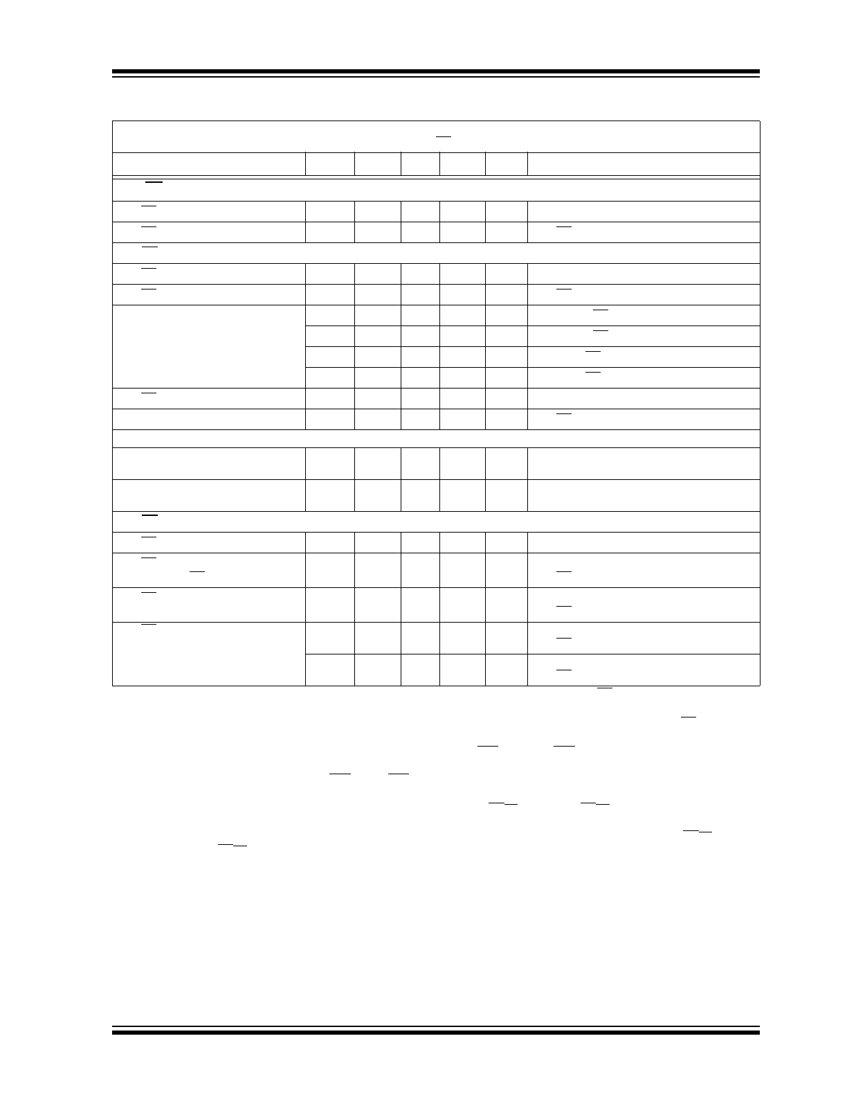
TABLE 1-1:
DC ELECTRICAL SPECIFICATIONS
Electrical Characteristics: Unless otherwise indicated, T
A
= +25°C, V
DD
= +2.5V to +5.5V, V
SS
= GND, V
CM
= V
DD
/3,
V
OUT
V
DD
/2, V
L
= V
DD
/2, R
L
= 1 k
to V
L
and CAL/CS = V
SS
(refer to
Figure 1-2
).
Parameters
Sym.
Min.
Typ.
Max.
Units
Conditions
Input Offset
Input Offset Voltage
V
OS
-200
—
+200
µV
After calibration (
Note 1
)
Input Offset Voltage Trim Step
V
OSTRM
—
37
200
µV
Input Offset Voltage Drift
V
OS
/
T
A
—
±2.5
—
µV/°C T
A
= -40°C to +125°C
Power Supply Rejection Ratio
PSRR
61
76
—
dB
Input Current and Impedance
Input Bias Current
I
B
—
6
—
pA
Across Temperature
I
B
—
130
—
pA
T
A
= +85°C
Across Temperature
I
B
—
1700
5,000
pA
T
A
= +125°C
Input Offset Current
I
OS
—
±1
—
pA
Common Mode Input Impedance
Z
CM
—
10
13
||9
—
||pF
Differential Input Impedance
Z
DIFF
—
10
13
||2
—
||pF
Common Mode
Common Mode Input Voltage Range
V
CMR
V
SS
0.3
—
V
DD
1.3
V
(
Note 2
)
Common Mode Rejection Ratio
CMRR
65
81
—
dB
V
DD
= 2.5V, V
CM
= -0.3 to 1.2V
CMRR
68
84
—
dB
V
DD
= 5.5V, V
CM
= -0.3 to 4.2V
Open-Loop Gain
DC Open-Loop Gain (large signal)
A
OL
88
114
—
dB
V
DD
= 2.5V, V
OUT
= 0.3V to 2.2V
A
OL
94
123
—
dB
V
DD
= 5.5V, V
OUT
= 0.3V to 5.2V
Output
Maximum Output Voltage Swing
V
OL
, V
OH
V
SS
+ 25
—
V
DD
25
mV
V
DD
= 2.5V, G = +2,
0.5V Input Overdrive
V
OL
, V
OH
V
SS
+ 50
—
V
DD
50
mV
V
DD
= 5.5V, G = +2,
0.5V Input Overdrive
Output Short-Circuit Current
I
SC
±50
±95
±145
mA
V
DD
= 2.5V (
Note 3
)
I
SC
±50
±100
±150
mA
V
DD
= 5.5V (
Note 3
)
Note 1:
Describes the offset (under the specified conditions) right after power-up, or just after the CAL/CS pin is toggled. Thus,
1/f noise effects (an apparent wander in V
OS
; see
Figure 2-35
) are not included.
2:
See
Figure 2-6
and
Figure 2-7
for temperature effects.
3:
The I
SC
specifications are for design guidance only; they are not tested.
MCP651/1S/2/3/4/5/9
DS20002146D-page 4
2009-2014 Microchip Technology Inc.
Calibration Input
Calibration Input Voltage Range
V
CALRNG
V
SS
+ 0.1
—
V
DD
– 1.4
mV
V
CAL
pin externally driven
Internal Calibration Voltage
V
CAL
0.31V
DD
0.33V
DD
0.35V
DD
V
CAL
pin open
Input Impedance
Z
CAL
—
100 || 5
—
k
||pF
Power Supply
Supply Voltage
V
DD
2.5
—
5.5
V
Quiescent Current per Amplifier
I
Q
3
6
9
mA
I
O
= 0
POR Input Threshold, Low
V
PRL
1.15
1.40
—
V
POR Input Threshold, High
V
PRH
—
1.40
1.65
V
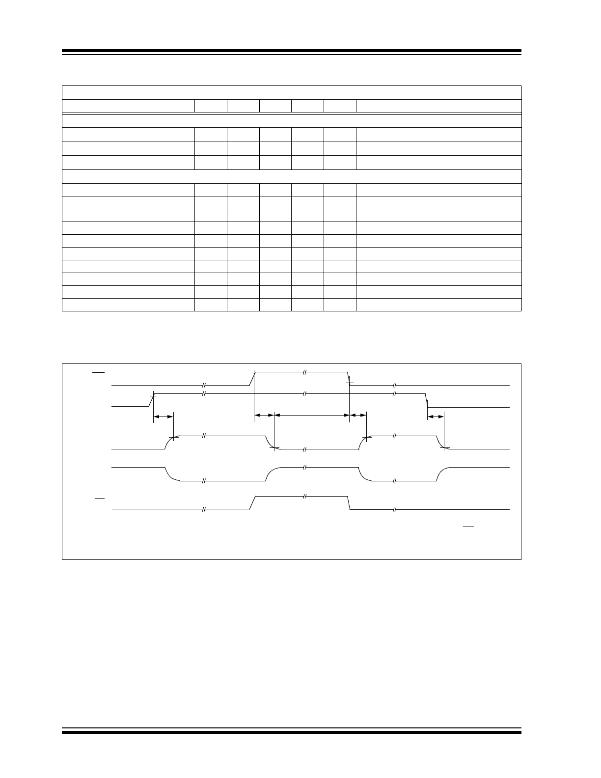
TABLE 1-2:
AC ELECTRICAL SPECIFICATIONS
Electrical Characteristics: Unless otherwise indicated, T
A
= 25°C, V
DD
= +2.5V to +5.5V, V
SS
= GND, V
CM
= V
DD
/2,
V
OUT
V
DD
/2, V
L
= V
DD
/2, R
L
= 1 k
to V
L
, C
L
= 20 pF and CAL/CS = V
SS
(refer to
Figure 1-2
).
Parameters
Sym.
Min.
Typ.
Max.
Units
Conditions
AC Response
Gain-Bandwidth Product
GBWP
—
50
—
MHz
Phase Margin
PM
—
65
—
°
G = +1
Open-Loop Output Impedance
R
OUT
—
20
—
AC Distortion
Total Harmonic Distortion plus Noise
THD+N
—
0.0012
—
%
G = +1, V
OUT
= 4V
P-P
, f = 1 kHz,
V
DD
= 5.5V, BW = 80 kHz
Step Response
Rise Time, 10% to 90%
t
r
—
6
—
ns
G = +1, V
OUT
= 100 mV
P-P
Slew Rate
SR
—
30
—
V/µs
G = +1
Noise
Input Noise Voltage
E
ni
—
17
—
µV
P-P
f = 0.1 Hz to 10 Hz
Input Noise Voltage Density
e
ni
—
7.5
—
nV/
Hz f = 1 MHz
Input Noise Current Density
i
ni
4
—
fA/
Hz f = 1 kHz
TABLE 1-1:
DC ELECTRICAL SPECIFICATIONS (CONTINUED)
Electrical Characteristics: Unless otherwise indicated, T
A
= +25°C, V
DD
= +2.5V to +5.5V, V
SS
= GND, V
CM
= V
DD
/3,
V
OUT
V
DD
/2, V
L
= V
DD
/2, R
L
= 1 k
to V
L
and CAL/CS = V
SS
(refer to
Figure 1-2
).
Parameters
Sym.
Min.
Typ.
Max.
Units
Conditions
Note 1:
Describes the offset (under the specified conditions) right after power-up, or just after the CAL/CS pin is toggled. Thus,
1/f noise effects (an apparent wander in V
OS
; see
Figure 2-35
) are not included.
2:
See
Figure 2-6
and
Figure 2-7
for temperature effects.
3:
The I
SC
specifications are for design guidance only; they are not tested.
2009-2014 Microchip Technology Inc.
DS20002146D-page 5
MCP651/1S/2/3/4/5/9
TABLE 1-3:
DIGITAL ELECTRICAL SPECIFICATIONS
Electrical Characteristics: Unless otherwise indicated, T
A
= 25°C, V
DD
= +2.5V to +5.5V, V
SS
= GND, V
CM
= V
DD
/2,
V
OUT
V
DD
/2, V
L
= V
DD
/2, R
L
= 1 k
to V
L
, C
L
= 20 pF and CAL/CS = V
SS
(refer to
Figure 1-1
and
Figure 1-2
).
Parameters
Sym.
Min.
Typ. Max. Units
Conditions
CAL/CS Low Specifications
CAL/CS Logic Threshold, Low
V
IL
V
SS
—
0.2V
DD
V
CAL/CS Input Current, Low
I
CSL
—
0
—
nA
CAL/CS = 0V
CAL/CS High Specifications
CAL/CS Logic Threshold, High
V
IH
0.8V
DD
V
DD
V
CAL/CS Input Current, High
I
CSH
—
0.7
—
µA
CAL/CS = V
DD
GND Current
I
SS
-3.5
-1.8
—
µA
Single, CAL/CS = V
DD
= 2.5V
I
SS
-8
-4
—
µA
Single, CAL/CS = V
DD
= 5.5V
I
SS
-5
-2.5
—
µA
Dual, CAL/CS = V
DD
= 2.5V
I
SS
-10
-5
—
µA
Dual, CAL/CS = V
DD
= 5.5V
CAL/CS Internal Pull-Down Resistor
R
PD
—
5
—
M
Amplifier Output Leakage
I
O(LEAK)
—
50
—
nA
CAL/CS = V
DD
POR Dynamic Specifications
V
DD
Low to Amplifier Off Time
(output goes High Z)
t
POFF
—
200
—
ns
G = +1 V/V, V
L
= V
SS
,
V
DD
= 2.5V to 0V step to V
OUT
= 0.1 (2.5V)
V
DD
High to Amplifier On Time
(including calibration)
t
PON
100
200
300
ms
G = +1 V/V, V
L
= V
SS
,
V
DD
= 0V to 2.5V step to V
OUT
= 0.9 (2.5V)
CAL/CS Dynamic Specifications
CAL/CS Input Hysteresis
V
HYST
—
0.25
—
V
CAL/CS Setup Time
(between CAL/CS edges)
t
CSU
1
—
—
µs
G = +1 V/V, V
L
= V
SS
(
Notes 2
,
3
,
4
)
CAL/CS = 0.8V
DD
to V
OUT
= 0.1 (V
DD
/2)
CAL/CS High to Amplifier Off Time
(output goes High Z)
t
COFF
—
200
—
ns
G = +1 V/V, V
L
= V
SS
,
CAL/CS = 0.8V
DD
to V
OUT
= 0.1 (V
DD
/2)
CAL/CS Low to Amplifier On Time
(including calibration)
t
CON
—
3
4
ms
G = +1 V/V, V
L
= V
SS
, MCP651 and MCP655,
CAL/CS = 0.2V
DD
to V
OUT
= 0.9 (V
DD
/2)
t
CON
—
6
8
ms
G = +1 V/V, V
L
= V
SS
, MCP659,
CAL/CS = 0.2V
DD
to V
OUT
= 0.9 (V
DD
/2)
Note 1:
The MCP652 single, MCP653 single, MCP655 dual and MCP659 quad have their CAL/CS inputs internally pulled down
to V
SS
(0V).
2:
This time ensures that the internal logic recognizes the edge. However, for the rising edge case, if CAL/CS is raised
before the calibration is complete, the calibration will be aborted and the part will return to Low-Power mode.
3:
For the MCP655 dual, there is an additional constraint. CAL
A
/CS
A
and CAL
B
/CS
B
can be toggled simultaneously
(within a time much smaller than t
CSU
) to make both op amps perform the same function simultaneously. If they are tog-
gled independently, then CAL
A
/CS
A
(CAL
B
/CS
B
) cannot be allowed to toggle while op amp B (op amp A) is in
Calibration mode; allow more than the maximum t
CON
time (4 ms) before the other side is toggled.
4:
For the MCP659 quad, there is an additional constraint. CAL
AD
/
CS
AD
and CAL
BC
/
CS
BC
can be toggled simultane-
ously (within a time much smaller than t
CSU
) to make all four op amps perform the same function simultaneously, and
the maximum t
CON
time is approximately doubled (8 ms). If they are toggled independently, then CAL
AD
/
CS
AD
(CAL
BC
/
CS
BC
) cannot be allowed to toggle while op amps B and C (op amps A and D) are in Calibration mode; allow
more than the maximum t
CON
time (8 ms) before the other side is toggled.
MCP651/1S/2/3/4/5/9
DS20002146D-page 6
2009-2014 Microchip Technology Inc.
1.3
Timing Diagram
FIGURE 1-1:
Timing Diagram.
TABLE 1-4:
TEMPERATURE SPECIFICATIONS
Electrical Characteristics: Unless otherwise indicated, all limits are specified for: V
DD
= +2.5V to +5.5V, V
SS
= GND.
Parameters
Sym.
Min.
Typ.
Max.
Units
Conditions
Temperature Ranges
Specified Temperature Range
T
A
-40
—
+125
°C
Operating Temperature Range
T
A
-40
—
+125
°C
(
Note 1
)
Storage Temperature Range
T
A
-65
—
+150
°C
Thermal Package Resistances
Thermal Resistance, 5L-2×3 SOT
JA
—
220.7
—
°C/W
Thermal Resistance, 6L-2×3 SOT
JA
—
190.5
—
°C/W
Thermal Resistance, 8L-2×3 TDFN
JA
—
52.5
—
°C/W
Thermal Resistance, 8L-3×3 DFN
JA
—
63
—
°C/W
(
Note 2
)
Thermal Resistance, 8L-SOIC
JA
—
163
—
°C/W
Thermal Resistance, 10L-3×3 DFN
JA
—
71
—
°C/W
(
Note 2
)
Thermal Resistance, 10L-MSOP
JA
—
202
—
°C/W
Thermal Resistance, 14L-SOIC
JA
—
95.3
—
°C/W
Thermal Resistance, 14L-TSSOP
JA
—
100
—
°C/W
Thermal Resistance, 16L-4x4-QFN
JA
—
46
—
°C/W
(
Note 2
)
Note 1:
Operation must not cause T
J
to exceed Maximum Junction Temperature specification (150°C).
2:
Measured on a standard JC51-7, four-layer printed circuit board with ground plane and vias.
High Z
V
DD
V
OUT
-3 µA (typical)
High Z
I
SS
I
CS
-3 µA (typical)
-6 mA (typical)
V
PRH
V
PRL
t
PON
t
POFF
On
0 nA (typical)
High Z
-3 µA (typical)
-6 mA (typical)
t
COFF
t
CON
On
0.7 µA (typical)
0 nA (typical)
CAL/CS
V
IH
V
IL
t
CSU
Note: For the MCP655 dual and the MCP659 quad, there is an additional constraint on toggling the two CAL/CS pins close
together; see the T
CON
specification in
Table 1-3
.
2009-2014 Microchip Technology Inc.
DS20002146D-page 7
MCP651/1S/2/3/4/5/9
1.4
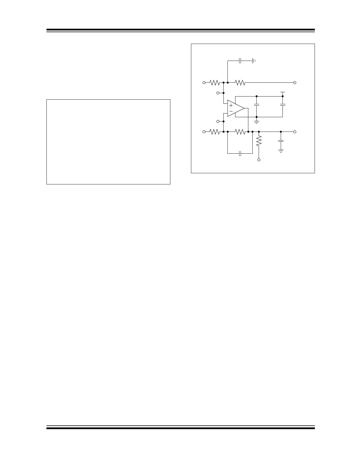
Test Circuits
The circuit used for most DC and AC tests is shown in
Figure 1-2
. This circuit can independently set V
CM
and
V
OUT
; see
Equation 1-1
. Note that V
CM
is not the
circuit’s Common mode voltage ((V
P
+ V
M
)/2), and that
V
OST
includes V
OS
plus the effects (on the input offset
error, V
OST
) of temperature, CMRR, PSRR and A
OL
.
EQUATION 1-1:
FIGURE 1-2:
AC and DC Test Circuit for
Most Specifications.
G
DM
R
F
R
G
=
V
C M
V
P
V
DD
2
+
2
=
V
OUT
V
DD
2
V
P
V
M
–
V
OST
1
G
DM
+
+
+
=
Where:
G
DM
= Differential Mode Gain
(V/V)
V
CM
= Op Amp’s Common Mode
Input Voltage
(V)
V
OST
= Op Amp’s Total Input Offset
Voltage
(mV)
V
OST
V
IN–
V
IN+
–
=
V
DD
MCP65X
R
G
R
F
V
OUT
V
M
C
B2
C
L
R
L
V
L
C
B1
10 k
10 k
R
G
R
F
V
DD
/2
V
P
10 k
10 k
20 pF
1 k
2.2 µF
100 nF
V
IN–
V
IN+
C
F
6.8 pF
C
F
6.8 pF
MCP651/1S/2/3/4/5/9
DS20002146D-page 8
2009-2014 Microchip Technology Inc.
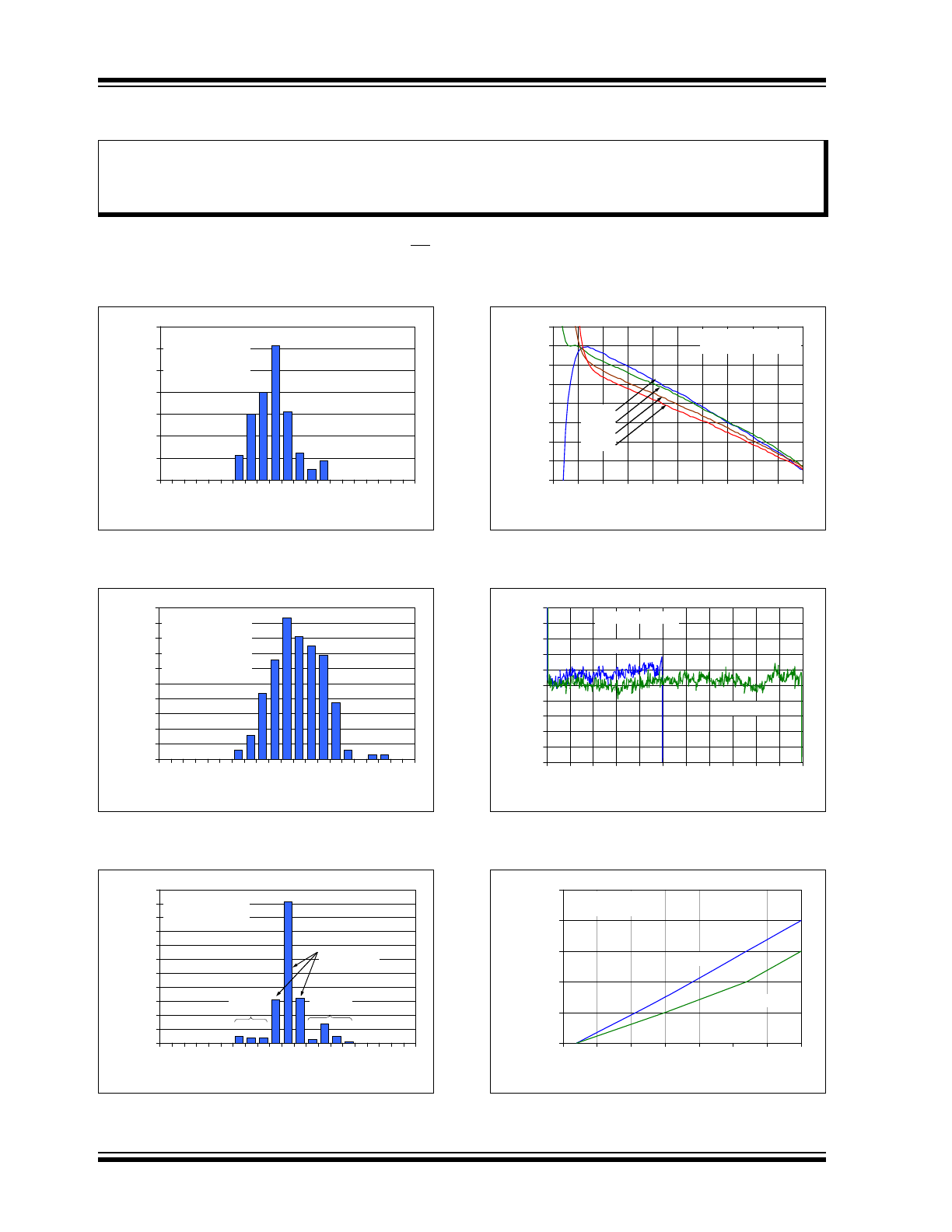
2.0
TYPICAL PERFORMANCE CURVES
Note: Unless otherwise indicated, T
A
= +25°C, V
DD
= +2.5V to 5.5V, V
SS
= GND, V
CM
= V
DD
/3, V
OUT
= V
DD
/2,
V
L
= V
DD
/2, R
L
= 1 k
to V
L
, C
L
= 20 pF, and CAL/CS = V
SS
.
2.1
DC Signal Inputs
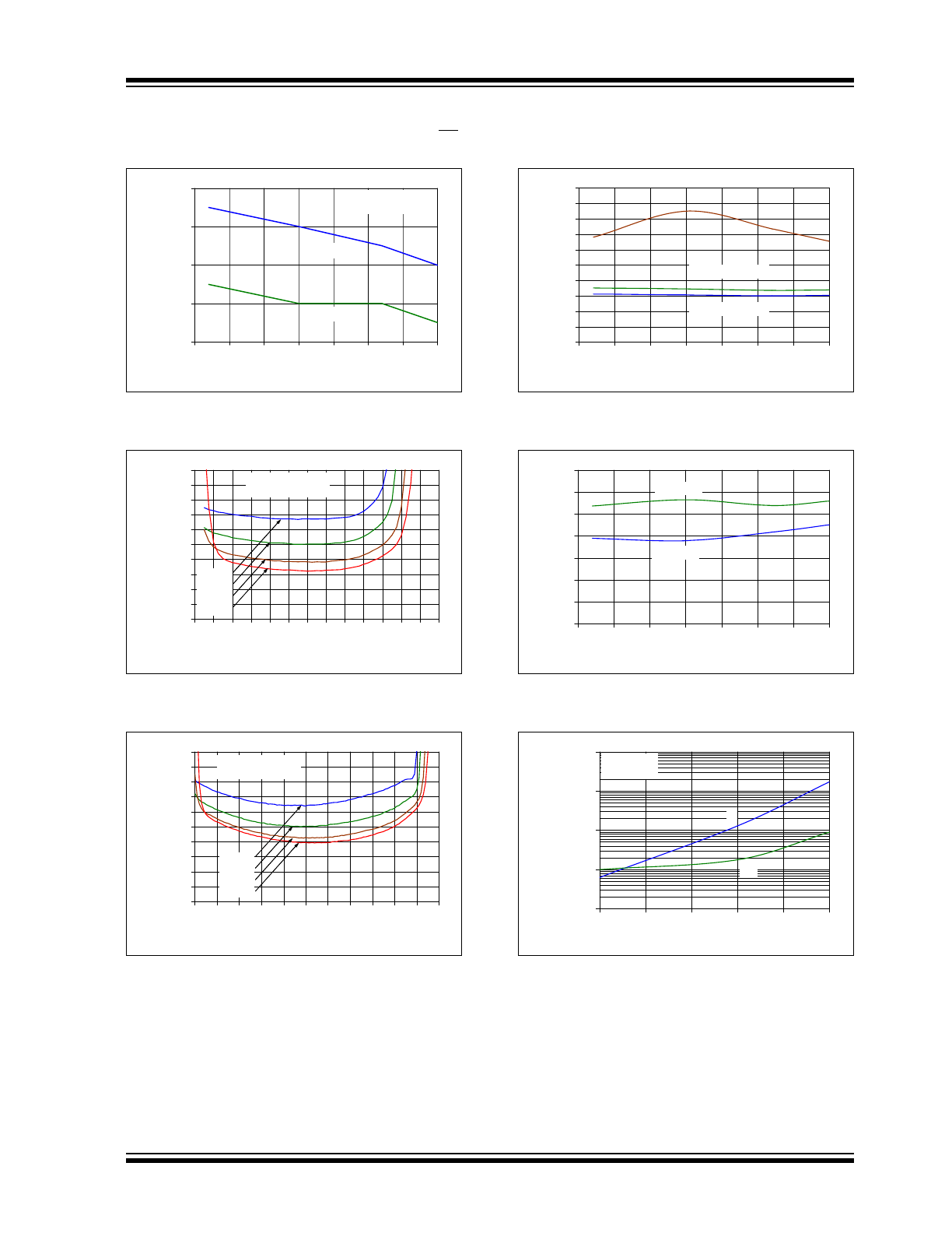
FIGURE 2-1:
Input Offset Voltage.
FIGURE 2-2:
Input Offset Voltage Drift.
FIGURE 2-3:
Input Offset Voltage
Repeatability (repeated calibration).
FIGURE 2-4:
Input Offset Voltage vs.
Power Supply Voltage.
FIGURE 2-5:
Input Offset Voltage vs.
Output Voltage.
FIGURE 2-6:
Low-Input Common Mode
Voltage Headroom vs. Ambient Temperature.
Note:
The graphs and tables provided following this note are a statistical summary based on a limited number of
samples and are provided for informational purposes only. The performance characteristics listed herein
are not tested or guaranteed. In some graphs or tables, the data presented may be outside the specified
operating range (e.g., outside specified power supply range) and therefore outside the warranted range.
0%
5%
10%
15%
20%
25%
30%
35%
-100 -80 -60 -40 -20
0
20
40
60
80 100
Input Offset Voltage (µV)
P
er
cent
age o
f O
ccur
re
nces
80 Samples
T
A
= +25°C
V
DD
= 2.5V and 5.5V
Calibrated at +25°C
0%
2%
4%
6%
8%
10%
12%
14%
16%
18%
20%
-10 -8
-6
-4
-2
0
2
4
6
8
10
Input Offset Voltage Drift (µV/°C)
Pe
rce
n
ta
ge o
f O
ccur
re
nce
s
80 Samples
V
DD
= 2.5V and 5.5V
T
A
= -40°C to +125°C
Calibrated at +25°C
0%
5%
10%
15%
20%
25%
30%
35%
40%
45%
50%
55%
-100 -80 -60 -40 -20
0
20
40
60
80 100
Input Offset Voltage Repeatability (µV)
P
e
rc
e
n
tag
e o
f Oc
cur
ren
ces
80 Samples
T
A
= +25°C
V
DD
= 2.5V and 5.5V
Calibration
Changed
Calibration
Changed
No Change
(includes noise)
-100
0
100
200
300
400
500
600
700
1.5 2.0 2.5 3.0 3.5 4.0 4.5 5.0 5.5 6.0 6.5
Power Supply Voltage (V)
Inp
u
t
Off
set V
o
lt
ag
e (µ
V
)
+125°C
+85°C
+25°C
-40°C
Representative Part
Calibrated at V
DD
= 6.5V
-50
-40
-30
-20
-10
0
10
20
30
40
50
0.0 0.5 1.0 1.5 2.0 2.5 3.0 3.5 4.0 4.5 5.0 5.5
Output Voltage (V)
In
p
u
t Off
set
V
o
lt
ag
e
(µ
V
)
V
DD
= 2.5V
V
DD
= 5.5V
Representative Part
-0.5
-0.4
-0.3
-0.2
-0.1
0.0
-50
-25
0
25
50
75
100
125
Ambient Temperature (°C)
L
o
w
I
npu
t C
o
m
m
o
n
M
ode
H
eadr
o
o
m
(
V
)
V
DD
= 2.5V
1 Lot
Low (V
CMR_L
– V
SS
)
V
DD
= 5.5V
2009-2014 Microchip Technology Inc.
DS20002146D-page 9
MCP651/1S/2/3/4/5/9
Note: Unless otherwise indicated, T
A
= +25°C, V
DD
= +2.5V to 5.5V, V
SS
= GND, V
CM
= V
DD
/3, V
OUT
= V
DD
/2,
V
L
= V
DD
/2, R
L
= 1 k
to V
L
, C
L
= 20 pF, and CAL/CS = V
SS
.
FIGURE 2-7:
High-Input Common Mode
Voltage Headroom vs. Ambient Temperature.
FIGURE 2-8:
Input Offset Voltage vs.
Common Mode Voltage with V
DD
= 2.5V.
FIGURE 2-9:
Input Offset Voltage vs.
Common Mode Voltage with V
DD
= 5.5V.
FIGURE 2-10:
CMRR and PSRR vs.
Ambient Temperature.
FIGURE 2-11:
DC Open-Loop Gain vs.
Ambient Temperature.
FIGURE 2-12:
Input Bias and Offset
Currents vs. Ambient Temperature with
V
DD
= +5.5V.
1.0
1.1
1.2
1.3
1.4
-50
-25
0
25
50
75
100
125
Ambient Temperature (°C)
H
ig
h
I
npu
t C
o
m
m
on
M
o
d
e
H
ead
ro
o
m
(
V
)
V
DD
= 2.5V
V
DD
= 5.5V
1 Lot
High (V
DD
– V
CMR_H
)
-1000
-800
-600
-400
-200
0
200
400
600
800
1000
-0.6
-0.4
-0.2
0.0
0.2
0.4
0.6
0.8
1.0
1.2
1.4
1.6
1.8
2.0
Input Common Mode Voltage (V)
Inp
u
t Off
set
V
o
ltag
e (
µ
V
)
V
DD
= 2.5V
Representative Part
-40°C
+25°C
+85°C
+125°C
-1000
-800
-600
-400
-200
0
200
400
600
800
1000
-0
.5
0.0
0.5
1.0
1.5
2.0
2.5
3.0
3.5
4.0
4.5
5.0
Input Common Mode Voltage (V)
In
put
O
ffset
V
o
lta
g
e (
µ
V
)
V
DD
= 5.5V
Representative Part
-40°C
+25°C
+85°C
+125°C
60
65
70
75
80
85
90
95
100
105
110
-50
-25
0
25
50
75
100
125
Ambient Temperature (°C)
CM
R
R
, PSR
R (
d
B)
PSRR
CMRR, V
DD
= 5.5V
CMRR, V
DD
= 2.5V
95
100
105
110
115
120
125
130
-50
-25
0
25
50
75
100
125
Ambient Temperature (°C)
DC Op
en
-L
o
o
p
Ga
in
(
d
B)
V
DD
= 5.5V
V
DD
= 2.5V
1
10
100
1,000
10,000
25
45
65
85
105
125
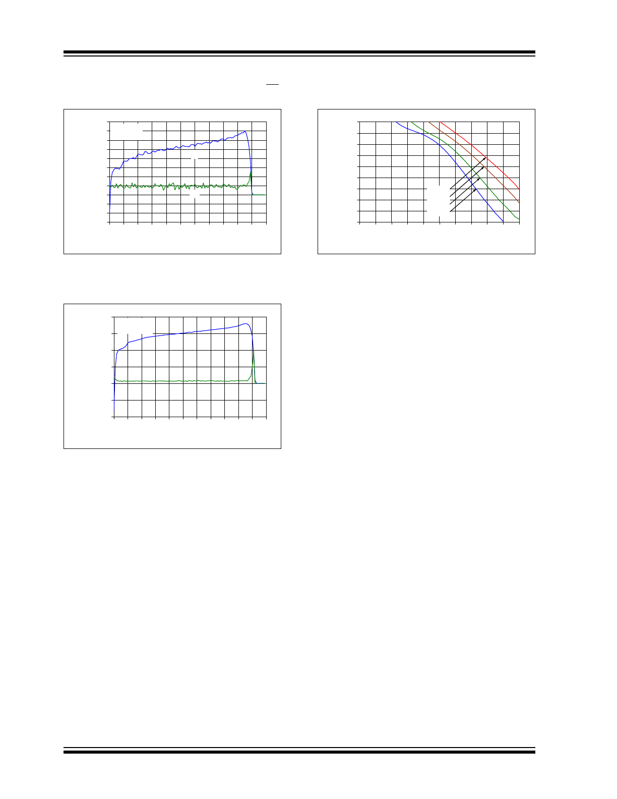
Ambient Temperature (°C)
In
put
B
ias,
Off
set
C
u
rr
en
ts
(p
A
)
V
DD
= 5.5V
V
CM
= V
CMR_H
-I
OS
I
B
MCP651/1S/2/3/4/5/9
DS20002146D-page 10
2009-2014 Microchip Technology Inc.
Note: Unless otherwise indicated, T
A
= +25°C, V
DD
= +2.5V to 5.5V, V
SS
= GND, V
CM
= V
DD
/3, V
OUT
= V
DD
/2,
V
L
= V
DD
/2, R
L
= 1 k
to V
L
, C
L
= 20 pF, and CAL/CS = V
SS
.
FIGURE 2-13:
Input Bias and Offset
Currents vs. Common Mode Input Voltage with
T
A
= +85°C.
FIGURE 2-14:
Input Bias and Offset
Currents vs. Common Mode Input Voltage with
T
A
= +125°C.
FIGURE 2-15:
Input Bias Current vs. Input
Voltage (below V
SS
).
-60
-40
-20
0
20
40
60
80
100
120
140
160
0.0 0.5 1.0 1.5 2.0 2.5 3.0 3.5 4.0 4.5 5.0 5.5
Common Mode Input Voltage (V)
In
put
B
ias, Off
set C
u
rr
ent
s
(p
A
)
I
B
T
A
= +85°C
V
DD
= 5.5V
I
OS
-1000
-500
0
500
1000
1500
2000
0.0 0.5 1.0 1.5 2.0 2.5 3.0 3.5 4.0 4.5 5.0 5.5
Common Mode Input Voltage (V)
Inp
u
t B
ias, O
ff
set C
u
rr
ent
s
(p
A
)
I
B
T
A
= +125°C
V
DD
= 5.5V
I
OS
1.E-12
1.E-11
1.E-10
1.E-09
1.E-08
1.E-07
1.E-06
1.E-05
1.E-04
1.E-03
-1.0 -0.9 -0.8 -0.7 -0.6 -0.5 -0.4 -0.3 -0.2 -0.1 0.0
Input Voltage (V)
Inpu
t
C
u
rr
ent Mag
n
it
ude (A
)
+125°C
+85°C
+25°C
-40°C
1m
100µ
10µ
1µ
100n
10n
1n
100p
10p
1p