
2012-2013 Microchip Technology Inc.
DS20002321C-page 1
MCP6491/2/4
Features
• Low-Input Bias Current
- 150 pA (typical, T
A
= +125°C)
• Low Quiescent Current
- 530 µA/amplifier (typical)
• Low-Input Offset Voltage
- ±1.5 mV (maximum)
• Supply Voltage Range: 2.4V to 5.5V
• Rail-to-Rail Input/Output
• Gain Bandwidth Product: 7.5 MHz (typical)
• Slew Rate: 6 V/µs (typical)
• Unity Gain Stable
• No Phase Reversal
• Small Packages
- Singles in SC70-5, SOT-23-5
• Extended Temperature Range
- -40°C to +125°C
Applications
• Photodiode Amplifier
• pH Electrode Amplifier
• Low Leakage Amplifier
• Piezoelectric Transducer Amplifier
• Active Analog Filter
• Battery-Powered Signal Conditioning
Design Aids
• SPICE Macro Models
• FilterLab
®
Software
• MAPS (Microchip Advanced Part Selector)
• Analog Demonstration and Evaluation Boards
• Application Notes
Description
The Microchip MCP6491/2/4 family of operational
amplifiers (op amps) has low-input bias current
(150 pA, typical at 125°C) and rail-to-rail input and
output operation. This family is unity gain stable and
has a gain bandwidth product of 7.5 MHz (typical).
These devices operate with a single-supply voltage as
low as 2.4V, while only drawing 530 µA/amplifier
(typical) of quiescent current. These features make the
family of op amps well suited for photodiode amplifier,
pH electrode amplifier, low leakage amplifier, and
battery-powered signal conditioning applications, etc.
The MCP6491/2/4 family is offered in single
(MCP6491), dual (MCP6492), quad (MCP6494)
packages. All devices are designed using an advanced
CMOS process and fully specified in extended
temperature range from -40°C to +125°C.
Related Parts
• MCP6471/2/4: 2 MHz, Low-Input Bias Current Op
Amps
• MCP6481/2/4: 4 MHz, Low-Input Bias Current Op
Amps
Package Types
5
4
1
2
3
V
DD
V
IN
+
V
SS
V
OUT
1
2
3
4
5
6
7
8
MCP6492
2x3 TDFN*
1
2
3
4
8
7
6
5
* Includes Exposed Thermal Pad (EP); see
Table 3-1
.
EP
9
1
2
3
4
11
12
13
14
5
4
1
2
3
MCP6491
SC70, SOT-23
MCP6494
SOIC, TSSOP
MCP6492
SOIC, MSOP
V
IN
–
V
OUTA
V
INA
–
V
INA
+
V
SS
V
INB
+
V
INB
–
V
OUTB
V
DD
V
OUTA
V
INA
–
V
INA
+
V
SS
V
INB
+
V
INB
–
V
OUTB
V
DD
5
6
7
8
9
10
V
OUTA
V
INA
–
V
INA
+
V
DD
V
INB
+
V
INB
–
V
OUTB
V
OUTC
V
OUTD
V
IND
–
V
INC
–
V
INC
+
V
IND
+
V
SS
7.5 MHz, Low-Input Bias Current Op Amps
MCP6491/2/4
DS20002321C-page 2
2012-2013 Microchip Technology Inc.
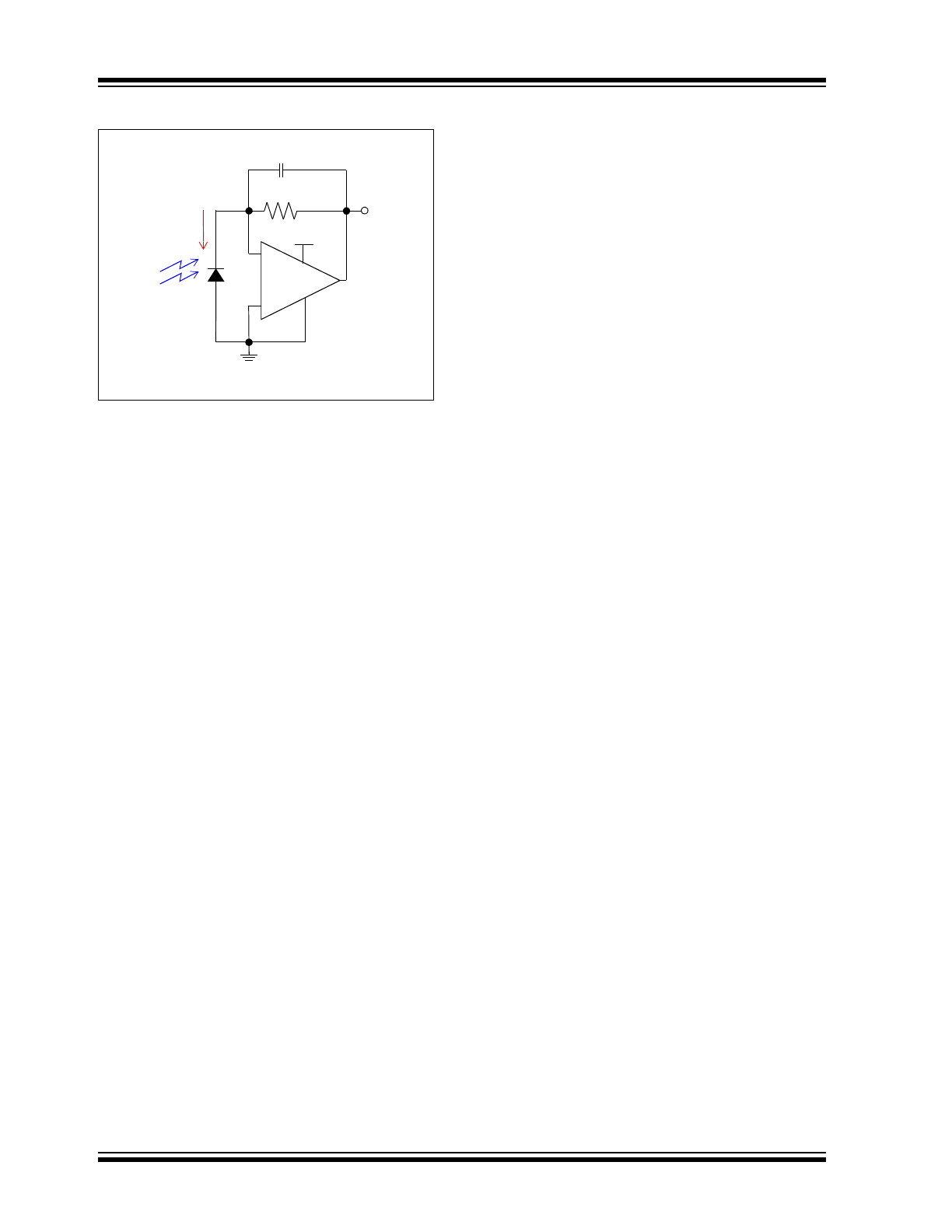
Typical Application
Photodiode Amplifier
D
1
Light
V
OUT
V
DD
R
2
C
2
I
D1
–
+
MCP649X
2012-2013 Microchip Technology Inc.
DS20002321C-page 3
MCP6491/2/4
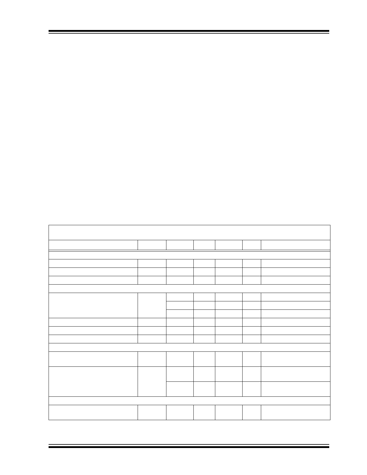
1.0
ELECTRICAL
CHARACTERISTICS
1.1
Absolute Maximum Ratings †
V
DD
– V
SS
................................................................................................................................... ......................................................6.5V
Current at Input Pins ................................................................................................................ ......................................................±2 mA
Analog Inputs (V
IN
+, V
IN
-) (
Note 1
) .................................................................................................................V
SS
– 1.0V to V
DD
+ 1.0V
All Other Inputs and Outputs ...........................................................................................................................V
SS
– 0.3V to V
DD
+ 0.3V
Difference Input Voltage...........................................................................................................................................................V
DD
– V
SS
Output Short-Circuit Current ................................................................................................................ ...................................continuous
Current at Output and Supply Pins ............................................................................................................... ..............................±60 mA
Storage Temperature ................................................................................................................ .....................................-65°C to +150°C
Maximum Junction Temperature (T
J
) ................................................................................................................ ...........................+150°C
ESD protection on all pins (HBM)
4 kV
Note 1: See
Section 4.1.2, Input Voltage Limits
.
† Notice: Stresses above those listed under “Absolute Maximum Ratings” may cause permanent damage to the device.
This is a stress rating only and functional operation of the device at those or any other conditions above those indicated
in the operational listings of this specification is not implied. Exposure to maximum rating conditions for extended
periods may affect device reliability.
1.2
Specifications
TABLE 1-1:
DC ELECTRICAL SPECIFICATIONS
Electrical Characteristics: Unless otherwise indicated, V
DD
= +2.4V to +5.5V, V
SS
= GND, T
A
= +25°C,
V
CM
= V
DD
/2, V
OUT
V
DD
/2, V
L
= V
DD
/2 and R
L
= 10 k
to V
L
. (Refer to
Figure 1-1
).
Parameters
Sym
Min
Typ
Max
Units
Conditions
Input Offset
Input Offset Voltage
V
OS
-1.5
—
+1.5
mV
V
DD
= 3.0V, V
CM
= V
DD
/4
Input Offset Drift with Temperature
V
OS
/
T
A
—
±2.5
—
µV/°C T
A
= -40°C to +125°C
Power Supply Rejection Ratio
PSRR
75
90
—
dB
V
CM
= V
DD
/4
Input Bias Current and Impedance
Input Bias Current
I
B
—
±1
—
pA
—
8
—
pA
T
A
= +85°C
—
150
350
pA
T
A
= +125°C
Input Offset Current
I
OS
—
±0.1
—
pA
Common Mode Input Impedance
Z
CM
—
10
13
||6
—
||pF
Differential Input Impedance
Z
DIFF
—
10
13
||6
—
||pF
Common Mode
Common Mode Input Voltage
Range
V
CMR
V
SS
- 0.3
—
V
DD
+ 0.3
V
Common Mode Rejection Ratio
CMRR
65
84
—
dB
V
CM
= -0.3V to 2.7V,
V
DD
= 2.4V
70
88
—
dB
V
CM
= -0.3V to 5.8V,
V
DD
= 5.5V
Open-Loop Gain
DC Open-Loop Gain (Large Signal)
A
OL
95
115
—
dB
0.2V < V
OUT
<(V
DD
– 0.2V)
V
DD
= 5.5V, V
CM
= V
SS
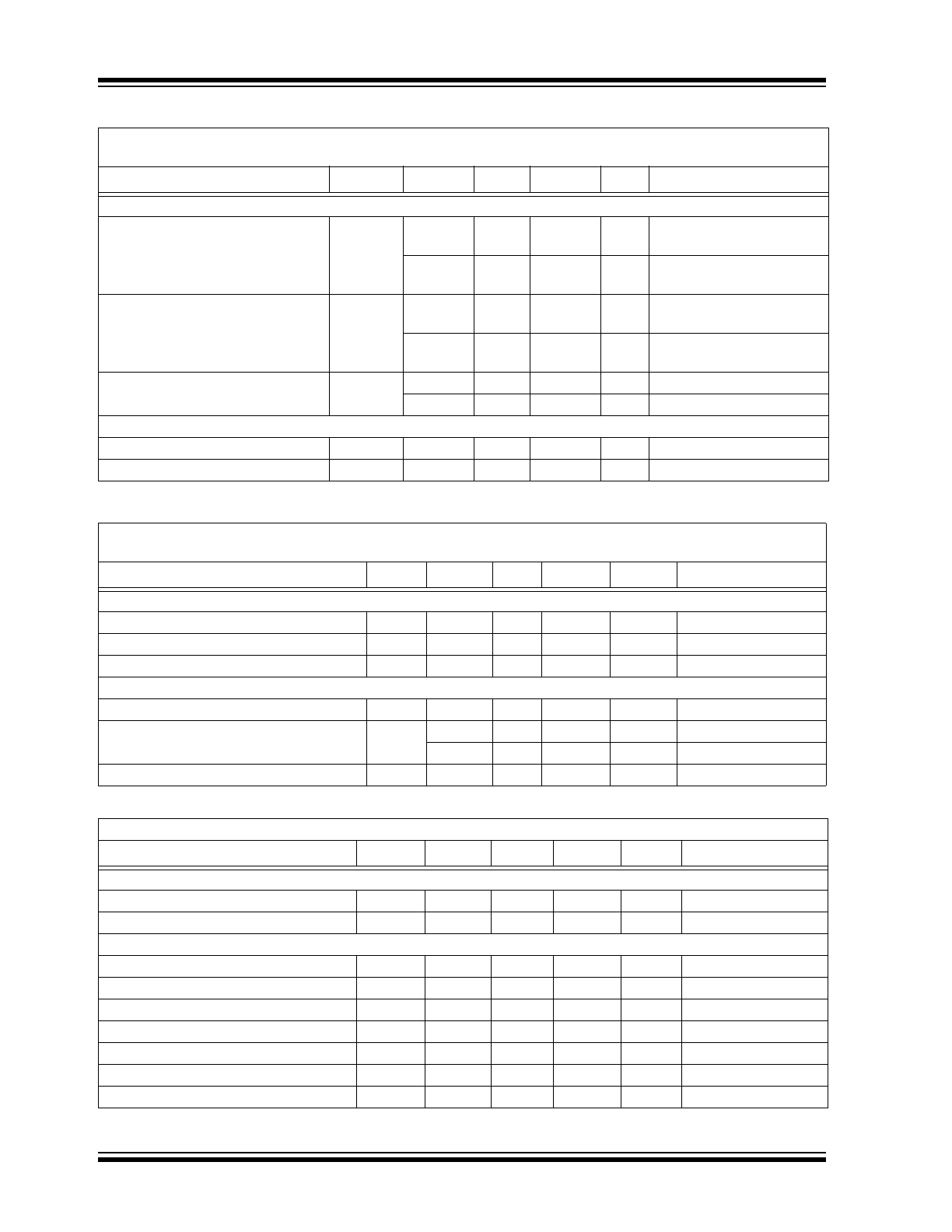
MCP6491/2/4
DS20002321C-page 4
2012-2013 Microchip Technology Inc.
Output
High-Level Output Voltage
V
OH
2.380
2.396
—
V
V
DD
= 2.4V
0.5V input overdrive
5.480
5.493
—
V
V
DD
= 5.5V
0.5V input overdrive
Low-Level Output Voltage
V
OL
—
0.004
0.020
V
V
DD
= 2.4V
0.5 V input overdrive
—
0.007
0.020
V
V
DD
= 5.5V
0.5 V input overdrive
Output Short-Circuit Current
I
SC
—
±15
—
mA
V
DD
= 2.4V
—
±40
—
mA
V
DD
= 5.5V
Power Supply
Supply Voltage
V
DD
2.4
—
5.5
V
Quiescent Current per Amplifier
I
Q
200
530
800
µA
I
O
= 0, V
CM
= V
DD
/4
TABLE 1-2:
AC ELECTRICAL SPECIFICATIONS
Electrical Characteristics: Unless otherwise indicated, T
A
= +25°C, V
DD
= +2.4V to +5.5V, V
SS
= GND,
V
CM
= V
DD
/2, V
OUT
V
DD
/2, V
L
= V
DD
/2, R
L
= 10 k
to V
L
and C
L
= 20 pF. (Refer to
Figure 1-1
).
Parameters
Sym
Min
Typ
Max
Units
Conditions
AC Response
Gain Bandwidth Product
GBWP
—
7.5
—
MHz
Phase Margin
PM
—
57
—
°
G = +1V/V
Slew Rate
SR
—
6
—
V/µs
Noise
Input Noise Voltage
E
ni
—
6
—
µVp-p
f = 0.1 Hz to 10 Hz
Input Noise Voltage Density
e
ni
—
19
—
nV/
Hz f = 1 kHz
—
14
—
nV/
Hz f = 10 kHz
Input Noise Current Density
i
ni
—
0.6
—
fA/
Hz
f = 1 kHz
TABLE 1-1:
DC ELECTRICAL SPECIFICATIONS (CONTINUED)
Electrical Characteristics: Unless otherwise indicated, V
DD
= +2.4V to +5.5V, V
SS
= GND, T
A
= +25°C,
V
CM
= V
DD
/2, V
OUT
V
DD
/2, V
L
= V
DD
/2 and R
L
= 10 k
to V
L
. (Refer to
Figure 1-1
).
Parameters
Sym
Min
Typ
Max
Units
Conditions
TABLE 1-3:
TEMPERATURE SPECIFICATIONS
Electrical Characteristics: Unless otherwise indicated, V
DD
= +2.4V to +5.5V and V
SS
= GND.
Parameters
Sym
Min
Typ
Max
Units
Conditions
Temperature Ranges
Operating Temperature Range
T
A
-40
—
+125
°C
Note 1
Storage Temperature Range
T
A
-65
—
+150
°C
Thermal Package Resistances
Thermal Resistance, 5L-SC-70
JA
—
331
—
°C/W
Thermal Resistance, 5L-SOT-23
JA
—
256
—
°C/W
Thermal Resistance, 8L-2x3 TDFN
JA
—
52.5
—
°C/W
Thermal Resistance, 8L-MSOP
JA
—
211
—
°C/W
Thermal Resistance, 8L-SOIC
JA
—
149.5
—
°C/W
Thermal Resistance, 14L-SOIC
JA
—
95.3
—
°C/W
Thermal Resistance, 14L-TSSOP
JA
—
100
—
°C/W
Note 1: The internal junction temperature (T
J
) must not exceed the absolute maximum specification of +150°C.
2012-2013 Microchip Technology Inc.
DS20002321C-page 5
MCP6491/2/4
1.3
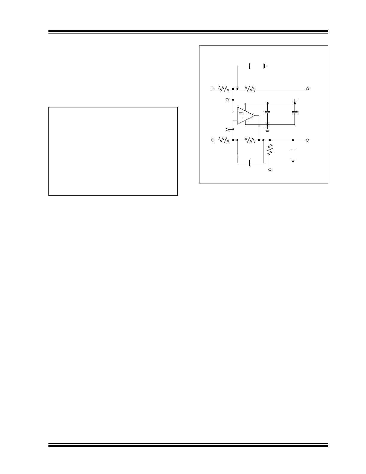
Test Circuits
The circuit used for most DC and AC tests is shown in
Figure 1-1
. This circuit can independently set V
CM
and
V
OUT
(refer to
Equation 1-1
). Note that V
CM
is not the
circuit’s common mode voltage ((V
P
+ V
M
)/2), and that
V
OST
includes V
OS
plus the effects (on the input offset
error, V
OST
) of temperature, CMRR, PSRR and A
OL
.
EQUATION 1-1:
FIGURE 1-1:
AC and DC Test Circuit for
Most Specifications.
G
DM
R
F
R
G
=
V
CM
V
P
V
DD
2
+
2
=
V
OUT
V
DD
2
V
P
V
M
–
V
OST
1
G
DM
+
+
+
=
Where:
G
DM
= Differential Mode Gain
(V/V)
V
CM
= Op Amp’s Common Mode
Input Voltage
(V)
V
OST
= Op Amp’s Total Input Offset
Voltage
(mV)
V
OST
V
IN +
V
IN–
–
=
V
DD
R
G
R
F
V
OUT
V
M
C
B2
C
L
R
L
V
L
C
B1
100 k
100 k
R
G
R
F
V
DD
/2
V
P
100 k
100 k
20 pF
10 k
1 µF
100 nF
V
IN–
V
IN+
C
F
6.8 pF
C
F
6.8 pF
MCP649X

MCP6491/2/4
DS20002321C-page 6
2012-2013 Microchip Technology Inc.
NOTES:
2012-2013 Microchip Technology Inc.
DS20002321C-page 7
MCP6491/2/4
2.0
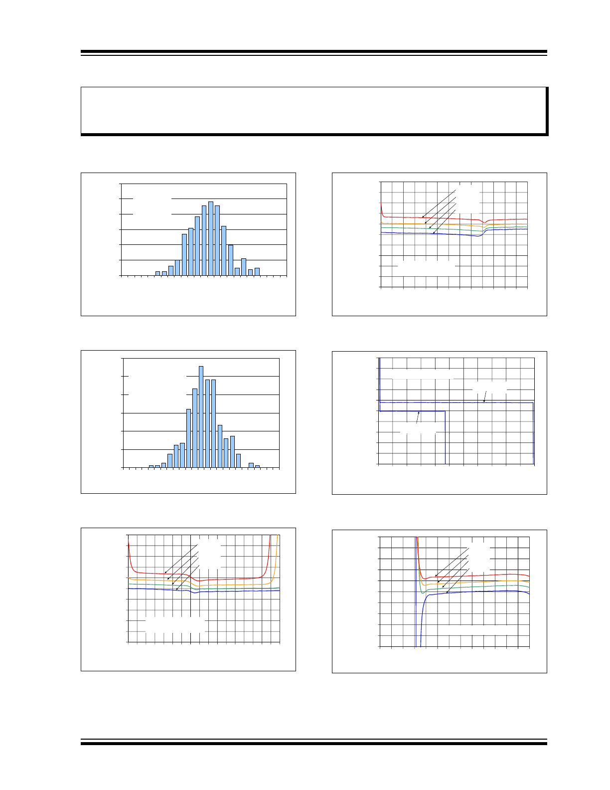
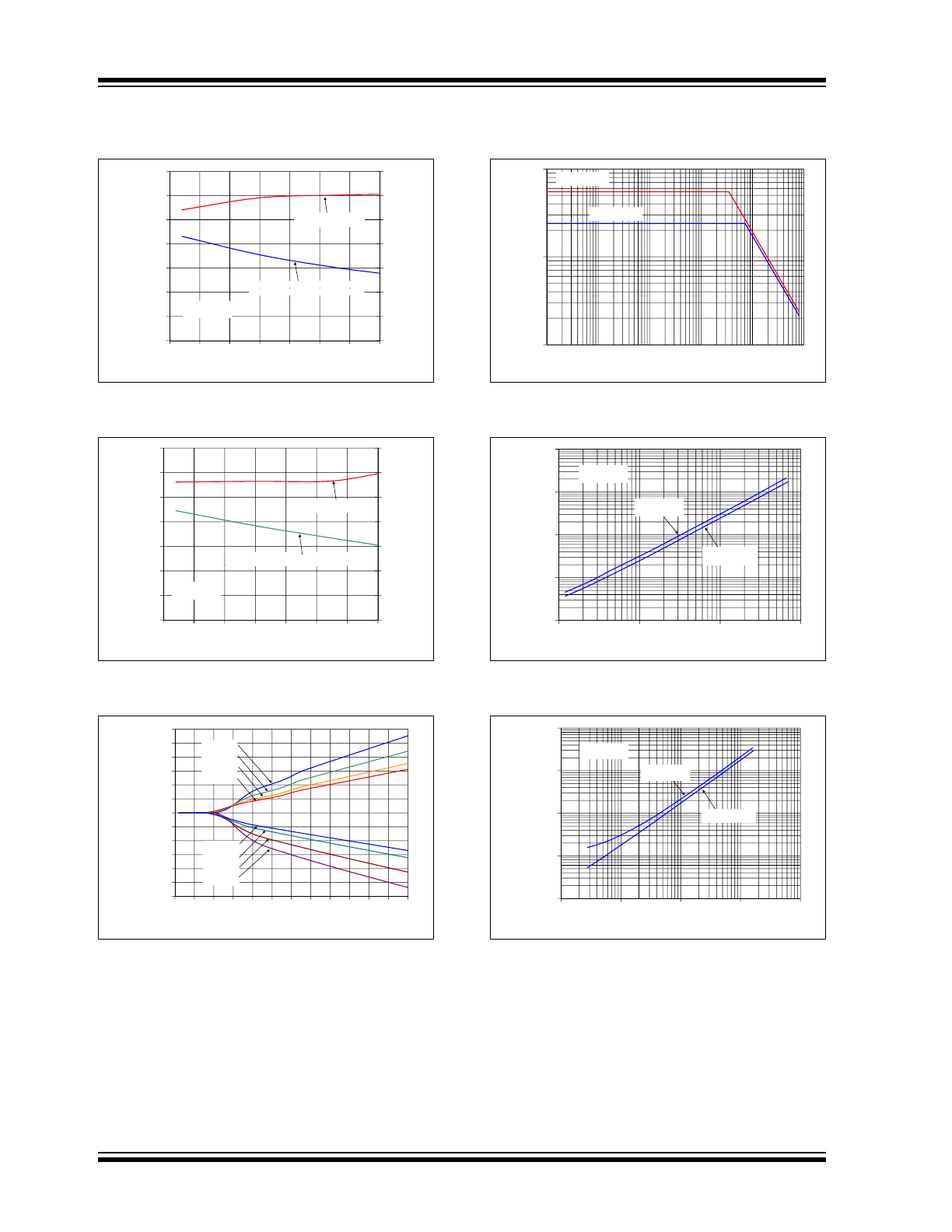
TYPICAL PERFORMANCE CURVES
Note: Unless otherwise indicated, T
A
= +25°C, V
DD
= +2.4V to +5.5V, V
SS
= GND, V
CM
= V
DD
/2, V
OUT
V
DD
/2,
V
L
= V
DD
/2, R
L
= 10 k
to V
L
and C
L
= 20 pF.
FIGURE 2-1:
Input Offset Voltage.
FIGURE 2-2:
Input Offset Voltage Drift.
FIGURE 2-3:
Input Offset Voltage vs.
Common Mode Input Voltage.
FIGURE 2-4:
Input Offset Voltage vs.
Common Mode Input Voltage.
FIGURE 2-5:
Input Offset Voltage vs.
Output Voltage.
FIGURE 2-6:
Input Offset Voltage vs.
Power Supply Voltage.
Note:
The graphs and tables provided following this note are a statistical summary based on a limited number of
samples and are provided for informational purposes only. The performance characteristics listed herein
are not tested or guaranteed. In some graphs or tables, the data presented may be outside the specified
operating range (e.g., outside specified power supply range) and therefore outside the warranted range.
0%
3%
6%
9%
12%
15%
18%
-1200
-1000
-800
-600
-400
-200
0
200
400
600
800
1000
1200
Percentage of Occurrences
Input Offset Voltage (µV)
270 Samples
V
DD
= 3.0V
V
CM
= V
DD
/4
0%
3%
6%
9%
12%
15%
18%
-12
-10
-8
-6
-4
-2
0
2
4
6
8
10
12
Percentage of Occurrences
Input Offset Voltage Drift (µV/°C)
270 Samples
V
DD
= 3.0V
V
CM
= V
DD
/4
T
A
= -40
°C to +125°C
-400
-200
0
200
400
600
800
1000
u
t Offset V
o
ltage
(µV)
+125°C
+85°C
+25°C
-40°C
-1000
-800
-600
-400
-0.5
-0.3
-0.1
0.1
0.3
0.5
0.7
0.9
1.1
1.3
1.5
1.7
1.9
2.1
2.3
2.5
2.7
2.9
Inp
u
Common Mode Input Voltage (V)
V
DD
= 2.4V
Representative Part
-400
-200
0
200
400
600
800
1000
u
t Offset V
o
ltage
(µV)
+125°C
+85°C
+25°C
-40°C
-1000
-800
-600
-400
-0.5
0.0
0.5
1.0
1.5
2.0
2.5
3.0
3.5
4.0
4.5
5.0
5.5
6.0
Inp
u
Common Mode Input Voltage (V)
V
DD
= 5.5V
Representative Part
-400
-200
0
200
400
600
800
1000
t Offset V
o
ltage
(µV)
V
DD
= 5.5V
V
DD
= 2.4V
Representative Part
-1000
-800
-600
400
0.0
0.5
1.0
1.5
2.0
2.5
3.0
3.5
4.0
4.5
5.0
5.5
Inpu
t
Output Voltage (V)
400
-200
0
200
400
600
800
1000
t Offset V
o
ltage
(µV)
+125°C
+85°C
+25°C
-40°C
-1000
-800
-600
-400
0.0
0.5
1.0
1.5
2.0
2.5
3.0
3.5
4.0
4.5
5.0
5.5
6.0
6.5
Inpu
t
Power Supply Voltage (V)
Representative Part
MCP6491/2/4
DS20002321C-page 8
2012-2013 Microchip Technology Inc.
Note: Unless otherwise indicated, T
A
= +25°C, V
DD
= +2.4V to +5.5V, V
SS
= GND, V
CM
= V
DD
/2, V
OUT
V
DD
/2,
V
L
= V
DD
/2, R
L
= 10 k
to V
L
and C
L
= 20 pF.
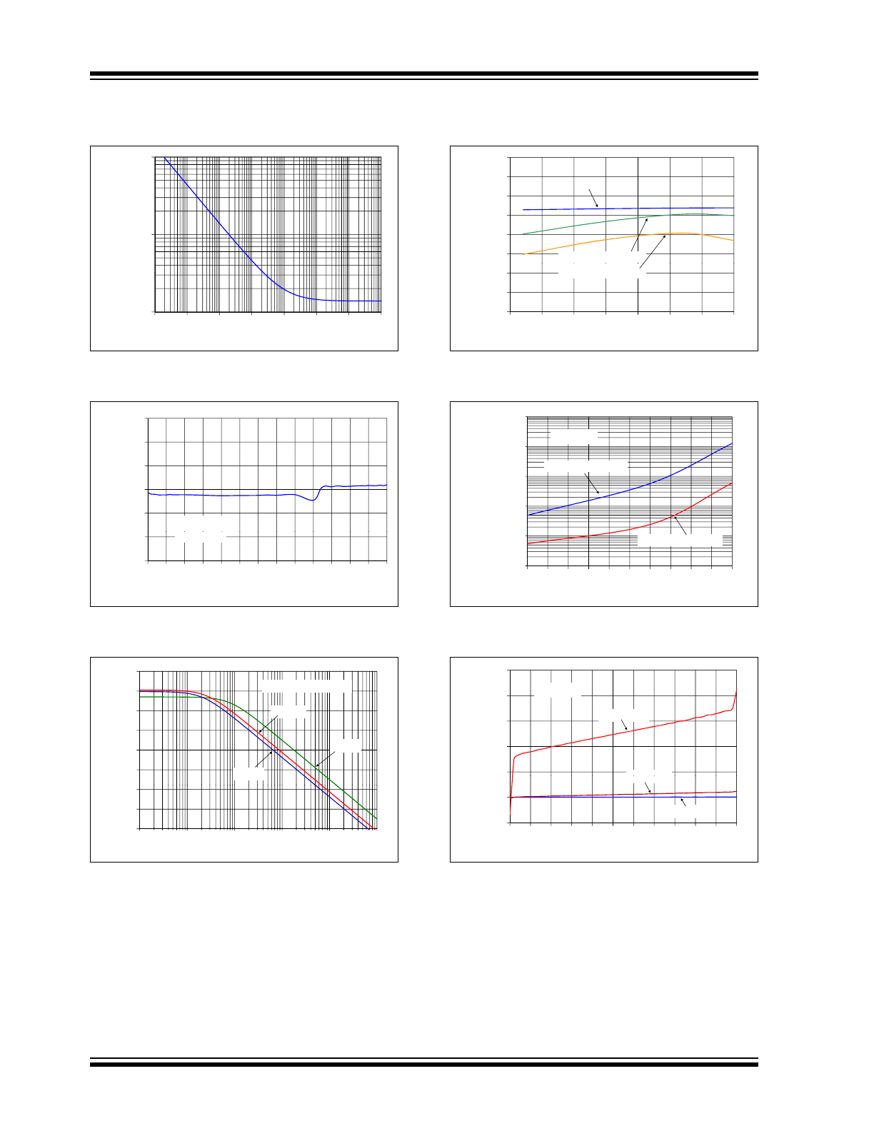
FIGURE 2-7:
Input Noise Voltage Density
vs. Frequency.
FIGURE 2-8:
Input Noise Voltage Density
vs. Common Mode Input Voltage.
FIGURE 2-9:
CMRR, PSRR vs.
Frequency.
FIGURE 2-10:
CMRR, PSRR vs. Ambient
Temperature.
FIGURE 2-11:
Input Bias, Offset Currents
vs. Ambient Temperature.
FIGURE 2-12:
Input Bias Current vs.
Common Mode Input Voltage.
100
1,000
N
oise V
o
ltage Density
(nV/
¥
Hz)
10
1.E-1 1.E+0 1.E+1 1.E+2 1.E+3 1.E+4 1.E+5 1.E+6
Input
N
Frequency (Hz)
0.1 1 10 100
1k
10k 100k 1M
10
15
20
25
30
V
o
ltage Noise Density
(nV/
¥
Hz)
f = 10 kHz
V
= 5 5 V
0
5
-0.5
0.0
0.5
1.0
1.5
2.0
2.5
3.0
3.5
4.0
4.5
5.0
5.5
6.0
Input
Common Mode Input Voltage (V)
V
DD
= 5.5 V
50
60
70
80
90
100
M
RR, PSRR
(dB)
Representative Part
CMRR
PSRR+
PSRR-
20
30
40
1.00E+01
1.00E+02
1.00E+03
1.00E+04
1.00E+05
1.00E+06
C
M
Frequency (Hz)
10 100 1k
10k
100k 1M
80
85
90
95
100
105
MRR, PSRR
(dB)
PSRR
CMRR @ V
DD
= 5.5V
65
70
75
-50
-25
0
25
50
75
100
125
C
Temperature (°C)
@ V
DD
= 2.4V
1
10
100
1000
a
nd Offset
Currents
(A)
Input Bias Current
V
DD
= 5.5 V
1n
100p
10p
1p
0.01
0.1
25
35
45
55
65
75
85
95
105
11
5
125
Input Bias
a
Ambient Temperature (°C)
Input Offset Current
0.1p
0.01p
50
100
150
200
250
u
t
Bias Current (pA)
T
A
= +125°C
T = +85°C
V
DD
= 5.5 V
-50
0
0.0
0.5
1.0
1.5
2.0
2.5
3.0
3.5
4.0
4.5
5.0
5.5
Inp
u
Common Mode Input Voltage (V)
T
A
= +85 C
T
A
= +25°C
2012-2013 Microchip Technology Inc.
DS20002321C-page 9
MCP6491/2/4
Note: Unless otherwise indicated, T
A
= +25°C, V
DD
= +2.4V to +5.5V, V
SS
= GND, V
CM
= V
DD
/2, V
OUT
V
DD
/2,
V
L
= V
DD
/2, R
L
= 10 k
to V
L
and C
L
= 20 pF.
FIGURE 2-13:
Quiescent Current vs.
Ambient Temperature.
FIGURE 2-14:
Quiescent Current vs.
Common Mode Input Voltage.
FIGURE 2-15:
Quiescent Current vs.
Common Mode Input Voltage.
FIGURE 2-16:
Quiescent Current vs.
Power Supply Voltage.
FIGURE 2-17:
Open-Loop Gain, Phase vs.
Frequency.
FIGURE 2-18:
DC Open-Loop Gain vs.
Ambient Temperature.
500
525
550
575
600
Q
uiescent Current
(µA/Amplifier)
V
DD
= 5.5V
V
DD
= 2.4V
450
475
500
-50
-25
0
25
50
75
100
125
Q
Ambient Temperature (°C)
DD
V
CM
= V
DD
/4
450
500
550
600
650
700
Quiescent Current
(µA/Amplifier)
300
350
400
-0.5
-0.3
-0.1
0.1
0.3
0.5
0.7
0.9
1.1
1.3
1.5
1.7
1.9
2.1
2.3
2.5
2.7
2.9
Common Mode Input Voltage (V)
V
DD
= 2.4V
450
500
550
600
650
700
Quiescent Current
(µA/Amplifier)
V
V
300
350
400
-0.5
0.0
0.5
1.0
1.5
2.0
2.5
3.0
3.5
4.0
4.5
5.0
5.5
6.0
Common Mode Input Voltage (V)
V
DD
= 5.5V
200
300
400
500
600
700
Q
uiescent Current
(µA/Amplifier)
+125°C
+85°C
+25°C
-40°C
0
100
200
0.0
0.5
1.0
1.5
2.0
2.5
3.0
3.5
4.0
4.5
5.0
5.5
6.0
6.5
Q
Power Supply Voltage (V)
V
CM
= V
DD
/4
-150
-120
-90
-60
-30
0
20
40
60
80
100
120
e
n-Loop Phase
(°)
e
n-Loop Gain (dB)
Open-Loop Gain
Open-Loop Phase
-210
-180
150
-20
0
20
1.0E+00
1.0E+01
1.0E+02
1.0E+03
1.0E+04
1.0E+05
1.0E+06
1.0E+07
1.0E+08
Op
e
Op
e
Frequency (Hz)
1 10 100 1k 10k 100k 1M 10M 100M
110
120
130
140
150
pen-Loop Gain (dB)
V
DD
= 2.4V
V
DD
= 5.5V
90
100
-50
-25
0
25
50
75
100
125
DC O
Temperature (°C)
MCP6491/2/4
DS20002321C-page 10
2012-2013 Microchip Technology Inc.
Note: Unless otherwise indicated, T
A
= +25°C, V
DD
= +2.4V to +5.5V, V
SS
= GND, V
CM
= V
DD
/2, V
OUT
V
DD
/2,
V
L
= V
DD
/2, R
L
= 10 k
to V
L
and C
L
= 20 pF.
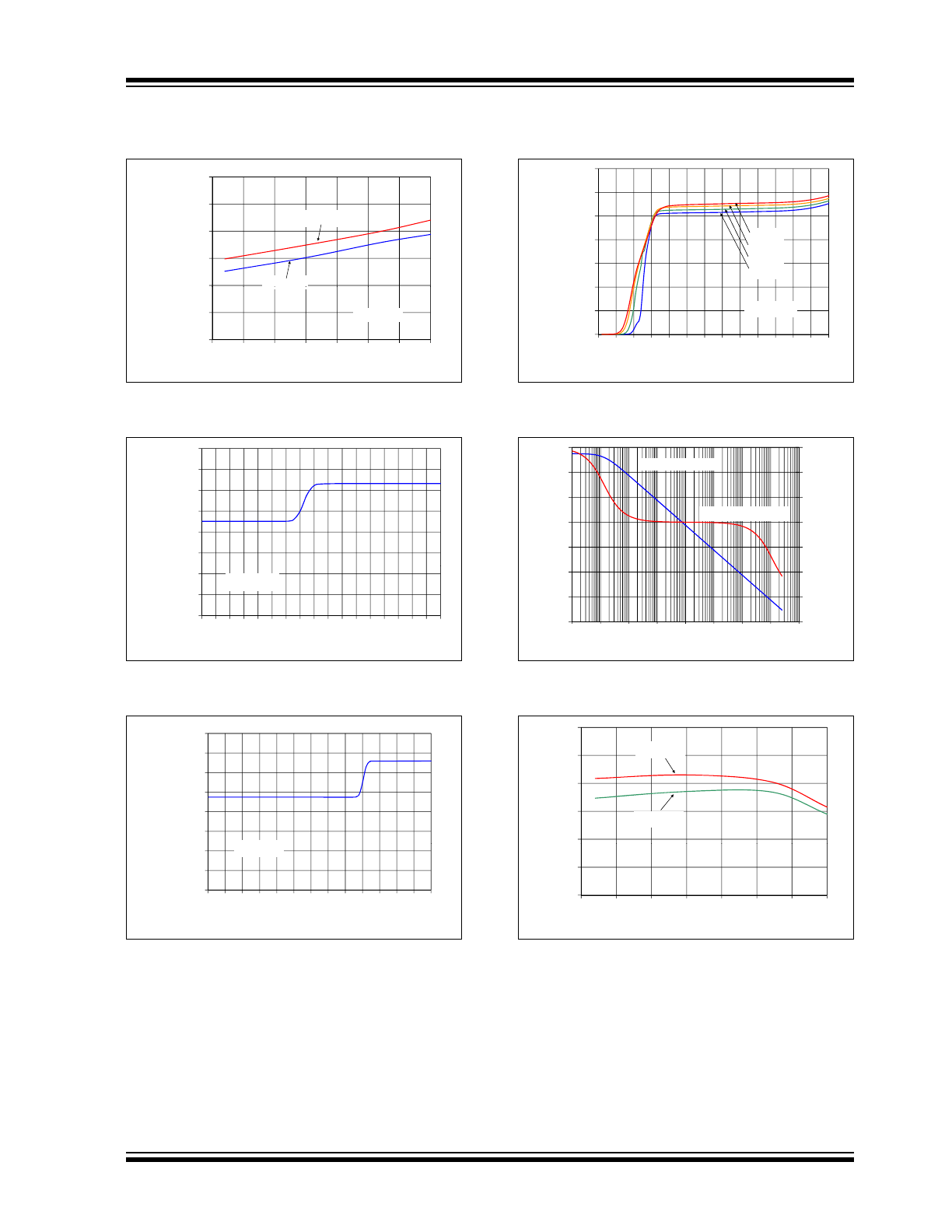
FIGURE 2-19:
Gain Bandwidth Product,
Phase Margin vs. Ambient Temperature.
FIGURE 2-20:
Gain Bandwidth Product,
Phase Margin vs. Ambient Temperature.
FIGURE 2-21:
Output Short Circuit Current
vs. Power Supply Voltage.
FIGURE 2-22:
Output Voltage Swing vs.
Frequency.
FIGURE 2-23:
Output Voltage Headroom
vs. Output Current.
FIGURE 2-24:
Output Voltage Headroom
vs. Output Current.
20
30
40
50
60
70
4
6
8
10
12
14
P
hase Margin (°)
n
Bandw
idth Product
(MHz)
Phase Margin
Gain Bandwidth Product
0
10
20
0
2
4
-50
-25
0
25
50
75
100
125
P
Gai
n
Ambient Temperature (°C)
V
DD
= 2.4V
Gain Bandwidth Product
30
40
50
60
70
6
8
10
12
14
P
hase Margin (°)
n
Bandw
idth Product
(MHz)
Phase Margin
Gain Bandwidth Product
0
10
20
0
2
4
-50
-25
0
25
50
75
100
125
P
Gai
n
Ambient Temperature (°C)
V
DD
= 5.5V
-20
-10
0
10
20
30
40
50
60
S
hort Circuit Current
(mA)
125°C
-40°C
+25°C
+85°C
+125°C
-60
-50
-40
-30
0.0
0.5
1.0
1.5
2.0
2.5
3.0
3.5
4.0
4.5
5.0
5.5
6.0
Output
S
Power Supply Voltage (V)
+125°C
+85°C
+25°C
-40°C
1
10
t V
o
ltage
Sw
ing (V
P-P
)
V
DD
= 2.4V
V
DD
= 5.5V
0.1
100
1000
10000
100000
1000000
10000000
Outpu
t
Frequency (Hz)
100 1k 10k 100k
1M 10M
10
100
1000
o
ltage Headroom (mV)
V
DD
- V
OH
V
OL
- V
SS
V
DD
= 2.4V
V
DD
- V
OH
V
OL
- V
SS
V
DD
= 2.4V
0.1
1
0.01
0.1
1
10
Output V
o
Output Current (mA)
10
100
1000
V
oltage Headroom (mV)
V
DD
- V
OH
V
OL
- V
SS
V
DD
= 5.5V
0.1
1
0.01
0.1
1
10
100
Output
V
Output Current (mA)