
2017 Microchip Technology Inc.
DS20005791B-page 1
MCP6411
Features:
• Low Quiescent Current:
47 μA
(typical)
• Low Input Offset Voltage:
- ±1.0 mV (maximum)
• Enhanced EMI Protection:
- Electromagnetic Interference Rejection Ratio
(EMIRR) at 1.8 GHz: 90 dB
• Supply Voltage Range: 1.7V to 5.5V
• Gain Bandwidth Product: 1 MHz (typical)
• Rail-to-Rail Input/Output
• Slew Rate: 0.5 V/μs (typical)
• Unity Gain Stable
• No Phase Reversal
• Small Packages: SC70-5, SOT-23-5
• Extended Temperature Range:
- -40°C to +125°C
Applications:
• Portable Medical Instruments
• Safety Monitoring
• Battery-Powered Systems
• Remote Sensing
• Supply Current Sensing
• Analog Active Filters
Design Aids:
• SPICE Macro Models
• FilterLab
®
Software
• Microchip Advanced Part Selector (MAPS)
• Analog Demonstration and Evaluation Boards
• Application Notes
Description:
The Microchip Technology Inc. MCP6411 operational
amplifier operates with a single supply voltage as low
as 1.7V, while drawing low quiescent current (55 μA,
maximum). This op amp also has low-input offset
voltage (±1.0 mV, maximum) and rail-to-rail input and
output operation. In addition, the MCP6411 is unity gain
stable and has a gain bandwidth product of 1 MHz
(typical). This combination of features supports
battery-powered and portable applications. The
MCP6411 has enhanced EMI protection to minimize
any electromagnetic interference from external
sources. This feature makes it well suited for EMI
sensitive applications such as power lines, radio
stations and mobile communications.
The MCP6411 is offered in small SC70-5 and
SOT-23-5 packages. All devices are designed using an
advanced CMOS process and fully specified in
extended temperature range from –40°C to +125°C.
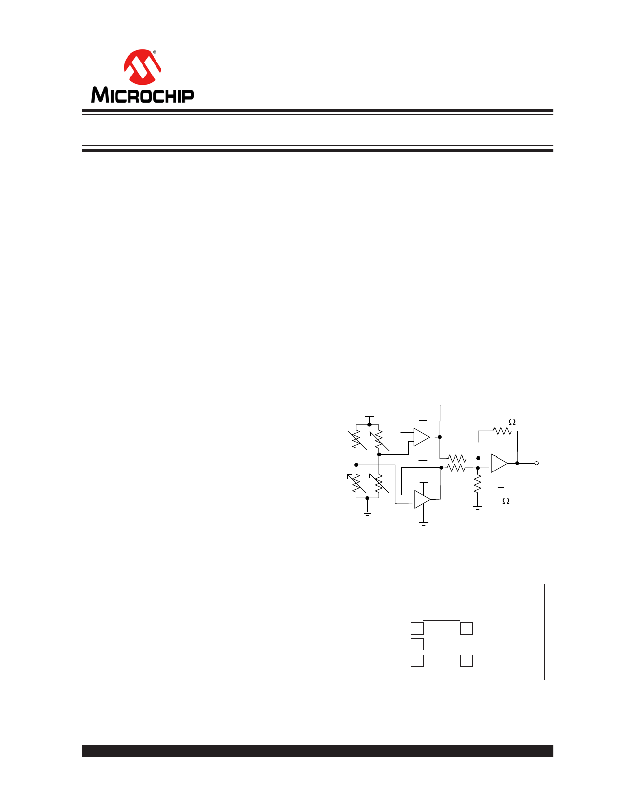
Typical Application
Package Types
V
DD
R
2
+
-
V
OUT
MCP64
1
R
1
R
3
100k
R
5
100k
1k
1k
R-¨R
R+¨R
V
a
V
b
V
DD
+
-
V
DD
+
-
MCP64
1
MCP64
1
R+¨R
R-¨R
V
DD
Strain Gauge
V
OUT
V
a
V
b
–
100k
1k
----------------
=
5
4
1
2
3
V
DD
V
IN
–
V
IN
+
V
SS
V
OUT
MCP6411
SC70-5, SOT-23-5
1 MHz Operational Amplifier with EMI Filtering

MCP6411
DS20005791B-page 2
2017 Microchip Technology Inc.
NOTES:
2017 Microchip Technology Inc.
DS20005791B-page 3
MCP6411
1.0
ELECTRICAL CHARACTERISTICS
1.1
Absolute Maximum Ratings †
V
DD
– V
SS
..................................................................................................................................................................6.5V
Current at Analog Input Pins (V
IN
+, V
IN
-)................................................................................................................±2 mA
Analog Inputs (V
IN
+, V
IN
-)†† .................................................................................................... V
SS
– 1.0V to V
DD
+ 1.0V
All Other Inputs and Outputs ................................................................................................... V
SS
– 0.3V to V
DD
+ 0.3V
Difference Input Voltage ................................................................................................................................ |V
DD
– V
SS
|
Output Short-Circuit Current ..........................................................................................................................Continuous
Current at Input Pins ...............................................................................................................................................±2 mA
Current at Output and Supply Pins ......................................................................................................................±30 mA
Storage Temperature .............................................................................................................................–65°C to +150°C
Maximum Junction Temperature (T
J
) ....................................................................................................................+150°C
ESD Protection on All Pins (HBM; MM)
4 kV; 400V
† Notice:
Stresses above those listed under “Absolute Maximum Ratings” may cause permanent damage to the device.
This is a stress rating only and functional operation of the device at those or any other conditions above those indicated
in the operational listings of this specification is not implied. Exposure to maximum rating conditions for extended
periods may affect device reliability.
††
See
Section 4.1.2 “Input Voltage Limits”
.
1.2
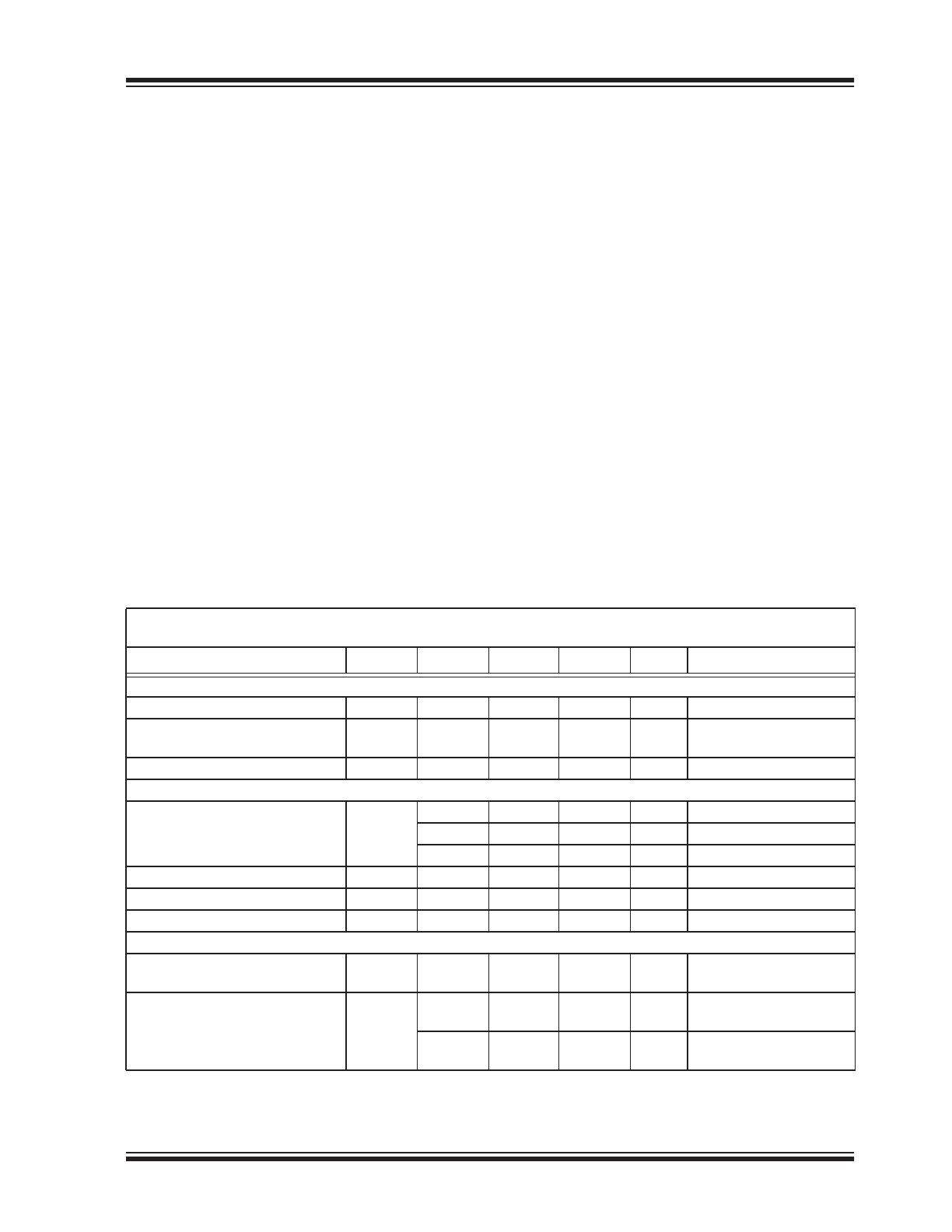
Specifications
TABLE 1-1:
DC ELECTRICAL SPECIFICATIONS
Electrical Characteristics
: Unless otherwise indicated, T
A
= +25°C, V
DD
= +1.72V to +5.5V, V
SS
= GND,
V
CM
= V
DD
/3, V
OUT
= V
DD
/2, V
L
= V
DD
/2, R
L
= 25 k
to V
L
and C
L
= 30 pF (refer to
Figure 1-1
).
Parameters
Sym.
Min.
Typ.
Max.
Units
Conditions
Input Offset
Input Offset Voltage
V
OS
–1.0
—
1.0
mV
V
DD
= 3.5V; V
CM
= V
DD
/4
Input Offset Drift with
Temperature
V
OS
/
T
A
—
±3.0
—
μV/°C T
A
= –40°C to +125°C,
V
CM
= V
SS
Power Supply Rejection Ratio
PSRR
75
90
—
dB
V
CM
= V
DD
/4
Input Bias Current and Impedance
Input Bias Current
I
B
—
±1
—
pA
—
20
—
pA
T
A
= +85°C
—
800
—
pA
T
A
= +125°C
Input Offset Current
I
OS
—
±1
—
pA
Common Mode Input Impedance
Z
CM
—
10
13
||12
—
||pF
Differential Input Impedance
Z
DIFF
—
10
13
||12
—
|pF
Common Mode
Common Mode Input Voltage
Range
V
CMR
V
SS
– 0.3
—
V
DD
+ 0.3
V
Common Mode Rejection Ratio
CMRR
75
90
—
dB
V
DD
= 5.5V
V
CM
= –0.3V to 5.8V
65
85
—
dB
V
DD
= 1.72V
V
CM
= –0.3V to 2.02V
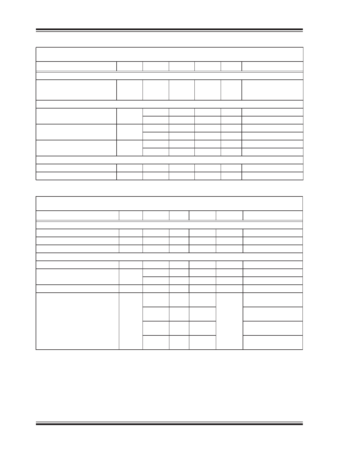
MCP6411
DS20005791B-page 4
2017 Microchip Technology Inc.
Open-Loop Gain
DC Open-Loop Gain
(Large Signal)
A
OL
95
115
—
dB
0.2 < V
OUT
< (V
DD
–0.2V)
V
CM
= V
DD
/4
V
DD
= 5.5V
Output
High-Level Output Voltage
V
OH
V
DD
– 5.5
V
DD
– 2
—
mV
V
DD
= 1.72V
V
DD
– 7
V
DD
– 3
—
mV
V
DD
= 5.5V
Low-Level Output Voltage
V
OL
—
V
SS
+ 2
V
SS
+ 5.5
mV
V
DD
= 1.72V
—
V
SS
+ 2.5 V
SS
+ 6.5
mV
V
DD
= 5.5V
Output Short-Circuit Current
I
SC
—
±6
—
mA
V
DD
= 1.72V
—
±22
—
mA
V
DD
= 5.5V
Power Supply
Supply Voltage
V
DD
1.72
—
5.5
V
Quiescent Current
I
Q
35
47
55
μA
I
O
= 0, V
CM
= V
DD
/4
TABLE 1-1:
DC ELECTRICAL SPECIFICATIONS (CONTINUED)
Electrical Characteristics
: Unless otherwise indicated, T
A
= +25°C, V
DD
= +1.72V to +5.5V, V
SS
= GND,
V
CM
= V
DD
/3, V
OUT
= V
DD
/2, V
L
= V
DD
/2, R
L
= 25 k
to V
L
and C
L
= 30 pF (refer to
Figure 1-1
).
Parameters
Sym.
Min.
Typ.
Max.
Units
Conditions
TABLE 1-2:
AC ELECTRICAL SPECIFICATIONS
Electrical Characteristics
: Unless otherwise indicated, T
A
= +25°C, V
DD
= +1.72V to +5.5V, V
SS
= GND,
V
CM
= V
DD
/3, V
OUT
= V
DD
/2, V
L
= V
DD
/2, R
L
= 25 k
to V
L
and C
L
= 30 pF (refer to
Figure 1-1
).
Parameters
Sym.
Min.
Typ.
Max.
Units
Conditions
AC Response
Gain Bandwidth Product
GBWP
—
1
—
MHz
Phase Margin
PM
—
68
—
°
G = +1 V/V
Slew Rate
SR
—
0.5
—
V/μs
Noise
Input Noise Voltage
E
ni
—
10
—
μV
P-P
f = 0.1 Hz to 10 Hz
Input Noise Voltage Density
e
ni
—
38
—
nV/
Hz
f = 1 kHz
—
32
—
nV/
Hz
f = 10 kHz
Input Noise Current Density
i
ni
—
0.6
—
fA/
Hz
f = 1 kHz
Electromagnetic Interference
Rejection Ratio
EMIRR
—
79
—
dB
V
IN
= 100 mV
PK
,
400 MHz
—
85
—
V
IN
= 100 mV
PK
,
900 MHz
—
90
—
V
IN
= 100 mV
PK
,
1800 MHz
—
94
—
V
IN
= 100 mV
PK
,
2400 MHz
2017 Microchip Technology Inc.
DS20005791B-page 5
MCP6411
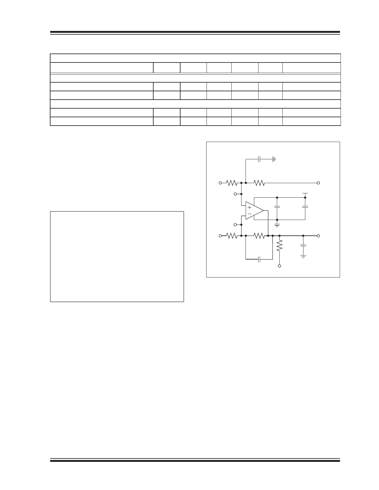
1.3
Test Circuits
The circuit used for most DC and AC tests is shown in
Figure 1-1
. This circuit can independently set V
CM
and
V
OUT
(see
Equation 1-1
). Note that V
CM
is not the
circuit’s Common mode voltage ((V
P
+ V
M
)/2), and that
V
OST
includes V
OS
plus the effects (on the input offset
error, V
OST
) of the temperature, CMRR, PSRR and
A
OL
.
EQUATION 1-1:
FIGURE 1-1:
AC and DC Test Circuit for
Most Specifications.
TABLE 1-3:
TEMPERATURE SPECIFICATIONS
Electrical Characteristics:
Unless otherwise indicated, V
DD
= +1.72V to +5.5V and V
SS
= GND.
Parameters
Sym.
Min.
Typ.
Max.
Units
Conditions
Temperature Ranges
Operating Temperature Range
T
A
-40
—
+125
°C
Note 1
Storage Temperature Range
T
A
-65
—
+150
°C
Thermal Package Resistances
Thermal Resistance, 5L-SC70
JA
—
331
—
°C/W
Thermal Resistance, 5L-SOT-23
JA
—
221
—
°C/W
Note 1:
The internal junction temperature (T
J
) must not exceed the absolute maximum specification of +150°C.
G
DM
R
F
R
G
=
V
CM
V
P
V
DD
2
+
2
=
V
OUT
V
DD
2
V
P
V
M
–
V
OST
1
G
DM
+
+
+
=
Where:
G
DM
= Differential Mode Gain
(V/V)
V
CM
= Op Amp’s Common Mode
Input Voltage
(V)
V
OST
= Op Amp’s Total Input Offset Voltage (mV)
V
OST
V
IN –
V
IN +
–
=
V
DD
R
G
R
F
V
OUT
V
M
C
B2
C
L
R
L
V
L
C
B1
100 k
100 k
R
G
R
F
V
DD
/2
V
P
100 k
100 k
30 pF
25 k
1 μF
100 nF
V
IN–
V
IN+
C
F
6.8 pF
C
F
6.8 pF
MCP6411

MCP6411
DS20005791B-page 6
2017 Microchip Technology Inc.
NOTES:
2017 Microchip Technology Inc.
DS20005791B-page 7
MCP6411
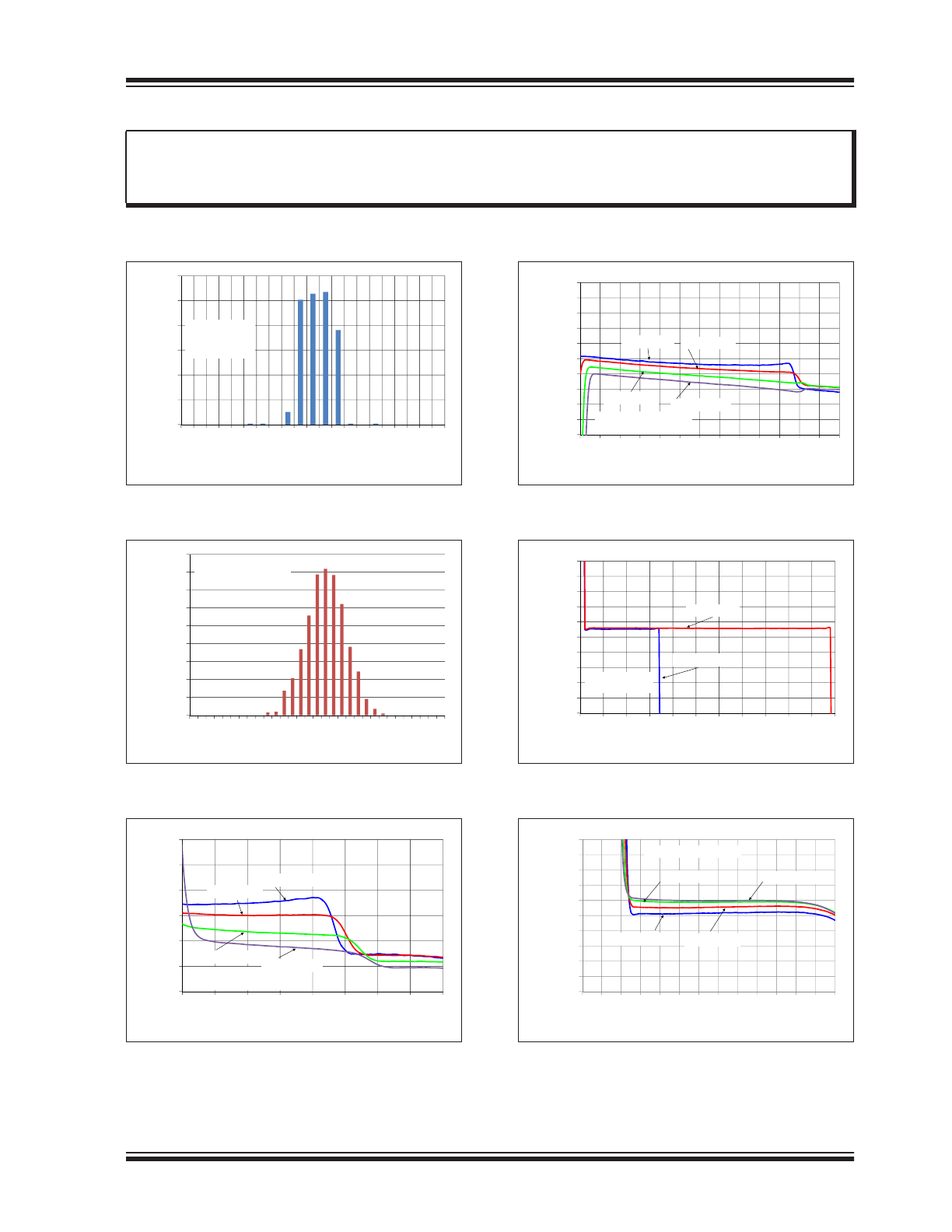
2.0
TYPICAL PERFORMANCE CURVES
Note:
Unless otherwise indicated, T
A
= +25°C, V
DD
= +1.72V to +5.5V, V
SS
= GND, V
CM
= V
DD
/3, V
OUT
= V
DD
/2,
V
L
= V
DD
/2, R
L
= 25 k
to V
L
and C
L
= 30 pF.
FIGURE 2-1:
Input Offset Voltage.
FIGURE 2-2:
Input Offset Voltage Drift.
FIGURE 2-3:
Input Offset Voltage vs.
Common Mode Input Voltage.
FIGURE 2-4:
Input Offset Voltage vs.
Common Mode Input Voltage.
FIGURE 2-5:
Input Offset Voltage vs.
Output Voltage.
FIGURE 2-6:
Input Offset Voltage vs.
Power Supply Voltage.
Note:
The graphs and tables provided following this note are a statistical summary based on a limited number of
samples and are provided for informational purposes only. The performance characteristics listed herein
are not tested or guaranteed. In some graphs or tables, the data presented may be outside the specified
operating range (e.g., outside specified power supply range) and therefore outside the warranted range.
0
5
10
15
20
25
30
-1
00
0
-9
00
-8
00
-7
00
-6
00
-5
00
-4
00
-3
00
-2
00
-1
00
0
100
200
300
400
500
600
700
800
900
1000
Percentage of
Occurances (%
)
Input Offset Voltage (μV)
1455 Samples
V
DD
= 3.5V
V
CM
= V
DD
/4
0%
2%
4%
6%
8%
10%
12%
14%
16%
18%
-1
5
-1
3
-1
1
-9
-7
-5
-3
-1
1
3
5
7
9
11
13
15
Percentage of
Occurrences
Input Offset Voltage Drift (μV/°C)
1000 Samples
T
A
= -40°C to +125°C
-600
-400
-200
0
200
400
600
-0.3
0
0.3
0.6
0.9
1.2
1.5
1.8
2.1
Input O
ffset V
o
ltage
(μV)
Common Mode Input Voltage (V)
V
DD
= 1.72V
Representative Part
T
A
= +125°C
T
A
= +85°C
T
A
= +25°C
T
A
= -40°C
-1000
-800
-600
-400
-200
0
200
400
600
800
1000
-0.5 0 0.5 1 1.5 2 2.5 3 3.5 4 4.5 5 5.5 6
Input O
ffset V
o
ltage
(μV)
Common Mode Input Voltage (V)
V
DD
= 5.5V
Representative Part
T
A
= +125°C
T
A
= +85°C
T
A
= +25°C
T
A
= -40°C
-1000
-800
-600
-400
-200
0
200
400
600
800
1000
0
0.5
1
1.5
2
2.5
3
3.5
4
4.5
5
5.5
Input Offset V
o
ltage
(μV)
Output Voltage (V)
Representative
Part
V
DD
= 5.5V
V
DD
= 1.72V
-1000
-800
-600
-400
-200
0
200
400
600
800
1000
0 0.5 1 1.5 2 2.5 3 3.5 4 4.5 5 5.5 6 6.5
Input
Of
fset V
o
ltage (
μ
V)
Power Supply Voltage (V)
Representative Part
T
A
= -40°C
T
A
= +25°C
T
A
= +85°C
T
A
= +125°C
MCP6411
DS20005791B-page 8
2017 Microchip Technology Inc.
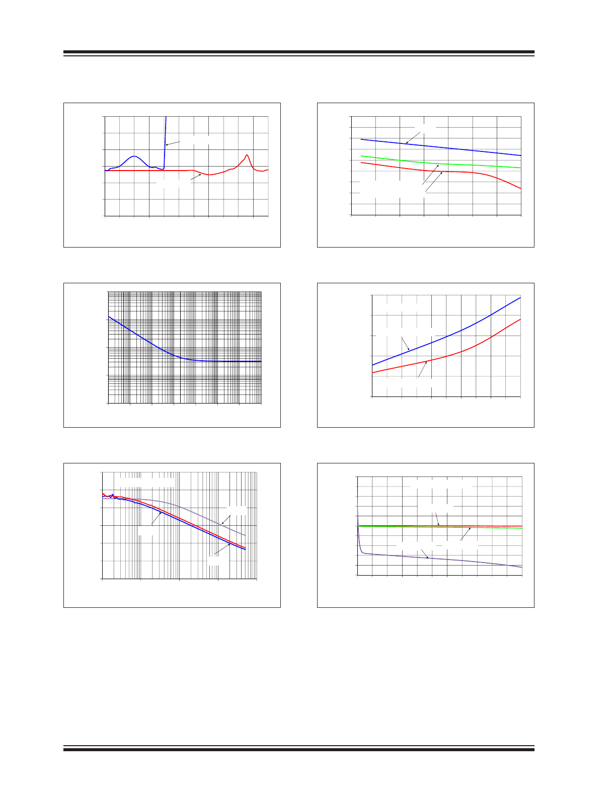
Note:
Unless otherwise indicated, T
A
= +25°C, V
DD
= +1.72V to +5.5V, V
SS
= GND, V
CM
= V
DD
/3, V
OUT
= V
DD
/2,
V
L
= V
DD
/2, R
L
= 25 k
to V
L
and C
L
= 30 pF.
FIGURE 2-7:
Input Noise Voltage Density
vs. Common Mode Input Voltage.
FIGURE 2-8:
Input Noise Voltage Density
vs. Frequency.
FIGURE 2-9:
CMRR, PSRR vs.
Frequency.
FIGURE 2-10:
CMRR, PSRR vs. Ambient
Temperature.
FIGURE 2-11:
Input Bias, Offset Current
vs. Ambient Temperature.
FIGURE 2-12:
Input Bias Current vs.
Common Mode Input Voltage.
0
10
20
30
40
50
60
0
0.5
1
1.5
2
2.5
3
3.5
4
4.5
5
5.5
Input Noise
V
o
ltage
Density
(nV/
¥
Hz)
Common Mode Input Voltage (V)
V
DD
= 1.72V
V
DD
= 5.5V
1
10
100
1000
10000
1.E-1 1.E+0 1.E+1 1.E+2 1.E+3 1.E+4 1.E+5 1.E+6
Input Noise
V
o
ltage
Density
(V/
¥
Hz)
Frequency (Hz)
0.1
1
10
100
1k
10k
100k
1M
10n
100n
1μ
1n
10μ
0
20
40
60
80
100
120
10
100
1,000
10,000
100,000
CMRR, PSRR (
d
B)
Frequency (Hz)
CMRR
PSRR-
PSRR+
Representative Part
50
60
70
80
90
100
110
120
130
140
-50
-25
0
25
50
75
100
125
CMRR, PSRR
(dB)
Ambient Temperature (°C)
PSSR
CMRR @ V
DD
= 5.5V
@ V
DD
= 1.72V
.01p
.10p
1.00p
10.00p
100.00p
1,000.00p
25
35
45
55
65
75
85
95 105 115 125
Input B
ias and
Offset
Currents
(A
)
Ambient Temperature (°C)
Input Offset Current
Input Bias Current
V
DD
= 5.5V
-1000
-800
-600
-400
-200
0
200
400
600
800
1000
0
0.5
1
1.5
2
2.5
3
3.5
4
4.5
5
5.5
Input Bias
Current
(pA)
Common Mode Input Voltage (V)
Representative Part
T
A
= +125°C
T
A
= +85°C
T
A
= +25°C
2017 Microchip Technology Inc.
DS20005791B-page 9
MCP6411
Note:
Unless otherwise indicated, T
A
= +25°C, V
DD
= +1.72V to +5.5V, V
SS
= GND, V
CM
= V
DD
/3, V
OUT
= V
DD
/2,
V
L
= V
DD
/2, R
L
= 25 k
to V
L
and C
L
= 30 pF.
FIGURE 2-13:
Quiescent Current vs.
Ambient Temperature.
FIGURE 2-14:
Quiescent Current vs.
Power Supply Voltage.
FIGURE 2-15:
Quiescent Current vs.
Common Mode Input Voltage.
FIGURE 2-16:
Quiescent Current vs.
Common Mode Input Voltage.
FIGURE 2-17:
Open-Loop Gain, Phase vs.
Frequency.
FIGURE 2-18:
DC Open-Loop Gain vs.
Ambient Temperature.
30
35
40
45
50
55
60
-50
-25
0
25
50
75
100
125
Q
u
iescent Current (μA)
Ambient Temperature (°C)
V
DD
= 5.5V
V
DD
= 1.72V
0
10
20
30
40
50
60
0
0.5
1
1.5
2
2.5
3
3.5
4
4.5
5
5.5
Qui
escent Current (μA)
Power Supply Voltage (V)
T
A
= +125°C
T
A
= -40°C
T
A
= +25°C
T
A
= +85°C
0
5
10
15
20
25
30
35
40
45
50
55
60
-0.5
0.5
1.5
2.5
Qui
escent Current (μA)
Common Mode Input Voltage (V)
V
DD
= 1.72V
G = +1 V/V
0
5
10
15
20
25
30
35
40
45
50
55
60
-0.5
0
0.5
1
1.5
2
2.5
3
3.5
4
4.5
5
5.5
Q
u
iescent Current (μA)
Common Mode Input Voltage (V)
V
DD
= 5.5V
G = +1 V/V
-315
-270
-225
-180
-135
-90
-45
0
45
-40
-20
0
20
40
60
80
100
120
1.E-11.E+01.E+11.E+21.E+31.E+41.E+51.E+61.E+7
O
p
en-
Loo
p
Phase
(°
)
Open-Loop Gain
(dB)
Frequency (Hz)
0.1
1
10
100
1k
10k 100k 1M 10M
Phase
Gain
V
DD
= 5.5V
V
DD
= 1.72V
80
90
100
110
120
130
140
-50
-25
0
25
50
75
100
125
DC O
p
en-Loop G
a
in
(dB)
Ambient Temperature (°C)
V
DD
= 5.5V
V
DD
= 1.72V
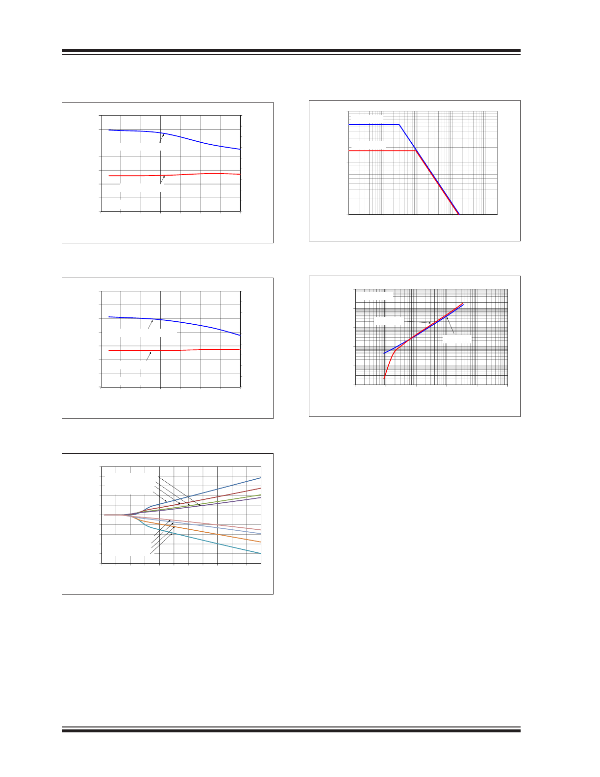
MCP6411
DS20005791B-page 10
2017 Microchip Technology Inc.
Note:
Unless otherwise indicated, T
A
= +25°C, V
DD
= +1.72V to +5.5V, V
SS
= GND, V
CM
= V
DD
/3, V
OUT
= V
DD
/2,
V
L
= V
DD
/2, R
L
= 25 k
to V
L
and C
L
= 30 pF.
FIGURE 2-19:
Gain Bandwidth Product,
Phase Margin vs. Ambient Temperature.
FIGURE 2-20:
Gain Bandwidth Product,
Phase Margin vs. Ambient Temperature.
FIGURE 2-21:
Output Short Circuit Current
vs. Power Supply Voltage.
FIGURE 2-22:
Output Voltage Swing vs.
Frequency.
FIGURE 2-23:
Output Voltage Headroom
vs. Output Current.
0
20
40
60
80
100
120
140
160
180
0.0
0.2
0.4
0.6
0.8
1.0
1.2
1.4
-50
-25
0
25
50
75
100
125
Phase Mar
g
in
(°C
)
G
a
in
Bandw
idth
Product
(MHz)
Ambient Temperature (°C)
V
DD
= 5.5V
Gain Bandwidth Product
Phase Margin
0
20
40
60
80
100
120
140
160
180
0.0
0.2
0.4
0.6
0.8
1.0
1.2
1.4
-50
-25
0
25
50
75
100
125
P
h
as
e Ma
rg
in
(°C
)
G
a
in
Bandw
idth
Product
(MHz)
Ambient Temperature (°C)
V
DD
= 1.72V
Gain Bandwidth Product
Phase Margin
-50
-40
-30
-20
-10
0
10
20
30
40
50
0
0.5
1
1.5
2
2.5
3
3.5
4
4.5
5
5.5
Output Shor
t
Circuit
Current
(m
A)
Power Supply Voltage (V)
ISC- @ T
A
= +125°C
T
A
= +85°C
T
A
= +25°C
T
A
= -40°C
ISC+ @ T
A
= +125°C
T
A
= +85°C
T
A
= +25°C
T
A
= -40°C
0.1
1
10
1000
10000
100000
1000000
10000000
Output V
o
ltage Swing (V
P-P
)
Frequency (Hz)
V
DD
= 1.72V
V
DD
= 5.5V
1k 10k 100k 1M 10M
0.01
0.1
1
10
100
1000
0.001
0.01
0.1
1
10
100
Output V
o
ltage
H
eadroom
(mV)
Output Current (mA)
V
DD
= 1.72V
V
DD
- V
OH
V
OL
- V
SS